The large-scale integration of electronic devices in silicon circuits has driven the technological revolution of the twentieth century. Over the last two decades, the field of photonics draws great efforts towards similar integration. The huge demand for bandwidth mandates broadband optical communication in ever increasing volumes at the rack, board, and chip levels.
The size, cost, and power consumption requirements of such large-scale deployment can only be met through the integration of multiple photonic functions within larger circuits. Silicon is often the platform of choice for photonic integration, due to the promise of compatibility with electronic circuits.
A primary objective of photonic signal processing is the direct selection of narrow frequency channels out of vast optical bandwidths, without electronic processing. However, narrowband analog filtering in the frequency domain mandates long temporal delays. For example, the selection of a 5 MHz-wide spectral channel requires that signals of interest are delayed by 200 ns. Such delay is far too long to accommodate using light on a chip: the speed of light is simply too fast. Light covers 20 meters of silicon waveguide during 200 ns, a path length that cannot be fitted in an integrated device. Even if one could fit such long paths within a silicon photonic circuit, the associated scattering losses would be prohibitively high.
"The solution," says Moshe Katzman from Bar-Ilan University, Israel, "may come in the way of surface acoustic waves. The speed of sound on the silicon chip is 50,000 times slower than that of light. If information could somehow be converted to an acoustic representation, the necessary long delays could be accumulated over compact, sub-mm path lengths." The delay of waveforms in the way of surface acoustic waves is known in analog electronics for decades. In those devices, information is converted from voltage to an acoustic wave based on the piezoelectric effect. However, photonic processing requires optical rather than electrical interfaces. In addition, the silicon substrate does not exhibit piezoelectricity.
Katzman continues: "Over the last few years, our group learned to rely on heat as means to excite surface acoustic waves within silicon photonic devices. Information-carrying light is absorbed in a grating of metallic patterns. Absorption leads to alternate heating and cooling of the metals, and to their thermal expansion and contraction. The resulting strain pattern is transferred to the silicon layer below and launches a surface acoustic wave. Information first takes up the form of modulated light, then of heat, and finally that of an acoustic wave. All processes take place in the standard silicon photonics platform."
Making full use of that concept, Dr. Moshe Katzman and co-authors from the group of Prof. Avi Zadok at Bar-Ilan University recently introduce opto-mechanics, the interactions between light and sound waves, to the key technological platform of standard silicon photonics. The concept overcomes the difficulty associated with the lack of piezoelectricity, and it is suitable to any substrate.
The microwave frequencies selected at the devices output can reach tens of GHz. The circuits are suitable for integrated photonic processing of analog waveforms. The related results were published in Photonics Research Volume. 10, Issue. 7, 2022 (Moshe Katzman, Maayan Priel, Inbar Shafir, Saawan Kumar Bag, Dvir Munk, Naor Inbar, Moshe Feldberg, Tali Sharabani, Leroy Dokhanian, Matan Slook, Avi Zadok. Surface acoustic wave photonic filters with a single narrow radio-frequency passband in standard silicon on insulator[J]. Photonics Research, 2022, 10(7): 1723).
The surface acoustic waves generated in the manner described above are effectively delayed on the silicon substrate for over 150 ns. During that time, multiple replicas of the information represented by the surface waves are imprinted on an optical readout wave. Information is thereby converted from one optical wave to another, via the slow-moving acoustic waves. As many as 32 replicas of the incoming information are effectively added together.
The combination of the large number of delayed copies is highly frequency-selective: Incident information is transferred to the device output near 2.5 GHz frequency, within a very narrow spectral range that is only 7 MHz wide (Figure 1). Compared with the very high frequencies of optical signals, the chosen bandwidth is narrower by a factor of 25 million. The selection of such a narrow range of frequencies directly in the optical domain is very difficult to realize on a silicon chip using light alone.
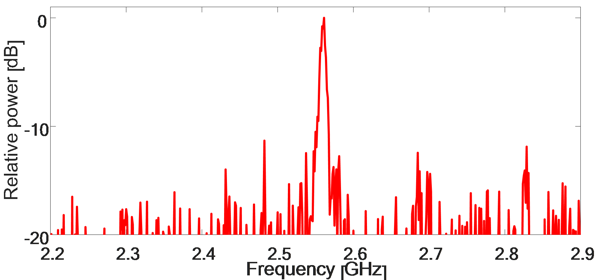
Figure 1 Measured normalized power transfer of signals through a surface acoustic wave-photonic device, as a function of their microwave frequency. Only a single narrow range of frequencies centered at 2.55 GHz is transmitted to the device output.
In another recent work by the same group (Hen et al., Opt. Express 30, 6949-6959 (2022)), the surface acoustic wave-photonic devices already served towards the analysis of elastic properties of thin layers.
Moshe Katzman concludes: "Acoustic waves have not been part of standard silicon photonic circuits until recently. We have found a way to introduce them. The acoustic waves buy us precious time. We have used this time to realize very narrowband filtering of optical signals, which is difficult to implement otherwise."