On the Cover
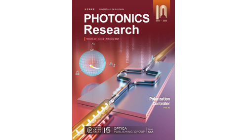
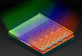
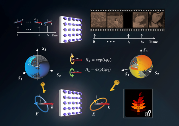
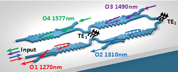
As a basic property of photons, polarization state (SOP) has been widely used in communication, optical coherence tomography, medical diagnosis, remote detection, material analysis and other fields. The polarization controller is the key element in the polarization applications, which can be realized by rotating wave plate and birefringence effect, but the traditional discrete optical components have some problems such as great volume, slow speed and poor reconfigurability. This cover article presents a novel polarization controller on the silicon substrate, which is ultra-compact, large tolerance and easy to regulate. The basic principle is that the horizontal and vertical polarization components of light waves can be converted into each other by using the mode hybrid effect of ridged silicon optical waveguide. By using MZI structure and phase shifter, the energy ratio and phase difference of two polarization components can be controlled, and the conversion between arbitrary polarization states can be realized. Due to the perfect symmetry of its structure, this work has obtained the highest range of polarization extinction ratio (PER) reported so far, and has wide application prospects in related fields.
Photonics Research
- Apr. 25, 2024
- Vol. 12, Issue 2 (2024)
On the Cover
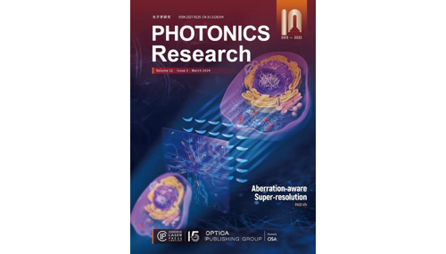
Ideal optical imaging relies upon the high-quality focusing of excitation light and accurate detection of the emission light from the fluorescent sample. However, both the optics in the microscope and the biological samples being investigated can introduce aberrations, thus causing degradation in resolution, loss of fluorescent photons, and deterioration of signal-to-background-ratio (SBR), etc. Moreover, microscopes with high numerical apertures (NA), especially the super-resolution microscopy, are more sensitive to aberrations, because the high-NA objectives are more susceptible to high-order aberrations. To detect and correct these optical aberrations, a large number of adaptive optics (AO) technologies have been explored in the last two decades. Conventional AO leverages specific devices, such as the Shack-Hartmann wavefront sensor to measure and correct optical aberrations, then utilized wavefront corrective devices such as spatial light modulators (SLMs) to compensate for the measured aberrations by reshaping the wavefronts. However, conventional AO complicates the optics, imaging procedures, and computation, resulting in many limitations in the actual imaging process.
Photonics Research
- Mar. 29, 2024
- Vol. 13, Issue 3 (2024)
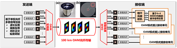
On the Cover
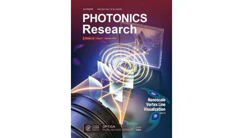
Vortex is one of the most common phenomena in nature. In 1992, Allen et al. proposed that such vortex beams carry orbital angular momentum (OAM), which has furthered the development of vortex beams in various fields, including optical tweezer, quantum communication and bio-image.
Photonics Research
- Mar. 25, 2024
- Vol. 12, Issue 1 (2024)
On the Cover
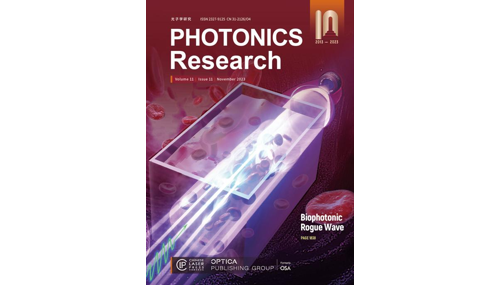
Rogue waves exist in various systems in nature. Rogue waves are unpredictable, featuring unique spatial-temporal distribution and statistics. When a light beam penetrates through a biological cell suspension, it experiences random phase and amplitude modulation, and its wavefront breaks up into multiple filaments. Under the random Brownian motion and nonlinear effects, these light filaments can constructively interfere and be spontaneously synchronized under proper conditions, and eventually a tiny portion of the filaments can form a rogue wave. Biophotonic rogue waves offer a new platform for the study of beam shaping and light-matter interaction dynamics in nonlinear soft-matter environment, which may find potential applications for health diagnosis using cell analysis.
Photonics Research
- Feb. 27, 2024
- Vol. 11, Issue 11 (2024)
On the Cover

Recommendation: Optical waveguides and metasurfaces offer two important platforms for light field manipulation in recent years. In photonic integrated circuits (PICs), light travels inside the waveguide in guided modes, and in-plane routing and out-of-plane coupling are realized on a tiny chip. It is highly compact but has limited free-space light controllability. On the other hand, metasurfaces, consisting of artificially designed subwavelength optical antennas, have unparalleled capability for engineering light with multiple degrees of freedom at the subwavelength scale. Here, two powerful platforms are synergically combined, and a novel spin-decoupled on-chip coupler is proposed with pure geometric metasurface, which provides a simple, efficient and multi-functional coupling interface for the interaction between guided and free-space modes.
Photonics Research
- Jan. 24, 2024
- Vol. 11, Issue 12 (2024)
On the Cover
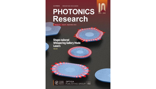
For the past two decades, researchers have explored dielectric cavities like spheres and disks, which support long-lived modes called whispering gallery modes (WGMs) due to total internal reflection along the cavity's boundary. WGMs in microcavities with high-Q and small mode volume are crucial for applications like low-threshold lasers, optical frequency combs, biosensors, and optical gyroscopes. However, the isotropic emission of 2D disk cavities limits their directional light emission. The rotational symmetry of the disk shape restricts practical applications of the photonic devices because of their isotropic emission which lacks directionality in far-field emission and difficulty in free space out-coupling. To overcome this problem, deformation of the disk cavity has been mainly attempted; however, the approach cannot avoid Q-degradation owing to the broken rotational symmetry.
Photonics Research
- Dec. 13, 2023
- Vol. 11, Issue 9 (2023)
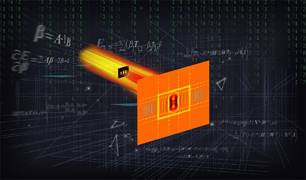
On the Cover
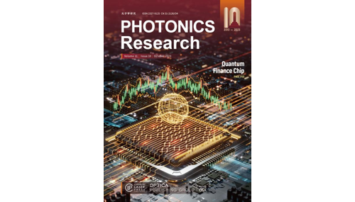
Recommendation: In the field of financial derivatives pricing, accurate and efficient computational methods are crucial. However, traditional option pricing models face great challenges in dealing with the increasing complexity of financial markets. Photonics computing chips, known for their high speed and low energy consumption, have attracted great attention. At the same time, quantum amplitude amplification algorithms provide the potential for quadratic speedup in option pricing. A collaborative research team from Hong Kong Polytechnic University and the National University of Singapore designed an efficient photonic computing chip dedicated to option pricing. The chip employs a unary option pricing algorithm, reducing the complexity of the photonic circuit compared to conventional binary algorithms, thus accelerating option pricing. The utilization of generative adversarial networks facilitates efficient learning and loading of asset distributions, accurately capturing market trends. This photonic computing chip offers the financial industry a rapid and accurate solution for option pricing, introducing new computational tools and opening new prospects for the commercial application of photonics computing technology.
Photonics Research
- Nov. 16, 2023
- Vol. 11, Issue 10 (2023)
On the Cover
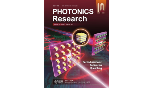
Nonlinear optical harmonic generation is of great significance in a broad range of technologies and has been attracting much attention in photonics, chemistry, and biosensing. Recently, with the advent of artificial electromagnetic materials, such as metamaterials and metasurfaces, that go beyond natural materials in many aspects, significant attention has been devoted to the nonlinear optical processes in artificial electromagnetic materials. In particular, epsilon-near-zero (ENZ) media with a vanishing permittivity are found to exhibit pronounced nonlinear optical properties. The ENZ media can provide large field enhancement due to the continuity of normal component of electric displacement field across the interface. Consequently, the ENZ media can give rise to unprecedented strong second-harmonic generation (SHG). Up to now, many theoretical and experimental works have demonstrated the SHG enhancement effect of the ENZ media.
Photonics Research
- Oct. 26, 2023
- Vol. 11, Issue 8 (2023)
On the Cover
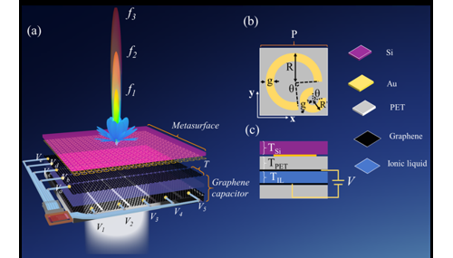
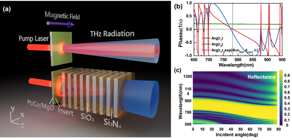
Terahertz (THz) waves are known as electromagnetic waves located between infrared rays and microwaves, and THz technology has made significant advances in biomedicine, non-destructive testing, imaging, and high-speed wireless communications. However, the lack of modulators is still one of the bottlenecks in the development of THz technology. Recently, researchers adopted metasurfaces based on tunable materials to solve this problem. Graphene is a two-dimensional tunable material. Since the band structure and optical properties of graphene can be modulated by applying a gate voltage, graphene becomes a good tunable optoelectronic material. Graphene-based active metasurfaces have the advantages of fast tuning speed, high transmittance, ultra-small thickness, and good response to THz waves due to intra-band transitions, which offer great application potential for THz wavefront control.
Photonics Research
- Sep. 06, 2023
- Vol. 11, Issue 7 (2023-)
On the Cover
Terahertz (THz) frequency occupies a unique position in the electromagnetic spectrum, serving as a transitional band between macro-scale electronics and micro-scale photonics. As an important electromagnetic wave, terahertz (THz) wave has strong practicability in non-destructive testing, wireless communication and imaging sensor technology. Ultra-high data rates in communication technology push toward exploring broadband and commercially available terahertz (THz) signal sources. The application and development of terahertz (THz) technology are largely limited by the level of THz sources. Therefore, obtaining stable and high-performance THz sources has been a major focus of current research.
Photonics Research
- Sep. 06, 2023
- Vol. 11, Issue 6 (2023-2024)
On the Cover
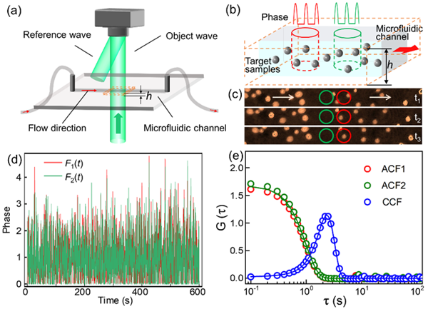
Characterizing the transport of nano- and microscopic particles (e.g., flow of blood cells in vessels and active movement of vesicles along microtubules in cells) is important for understanding many biological processes. A variety of techniques have been proposed to quantify the dynamics of particle flow, including particle image velocimetry (PIV) and Doppler optical coherence tomography (DOCT). PIV, which involves continuous imaging of particles to analyze the speed and direction of the flow pattern, is limited to sparse tracer particles. DOCT utilizes low coherence interference and Doppler frequency shift analysis to detect the blood flow in blood vessels, and currently, the time resolution of ODT is mainly limited by the necessity to record hundreds of holograms for each swept wavelength. Fluorescence correlation spectroscopy (FCS), especially the dual-focus FCS proposed in recent years, has also proven to be a valuable tool for the quantitative assessment of particle flow. In dual-focus FCS, the fluorescence signals from the two foci are registered as a function of time; then, time autocorrelation analysis of the intensity yields quantitative information about diffusion and flow. However, both FCS and dual-focus FCS require either intrinsically fluorescent particles, or particles labeled with fluorescent moieties. The unavoidable photobleaching sets limits to its application and calls for techniques not relying on fluorescence.
Photonics Research
- Jul. 18, 2023
- Vol. 11, Issue 5 (2023)
On the Cover
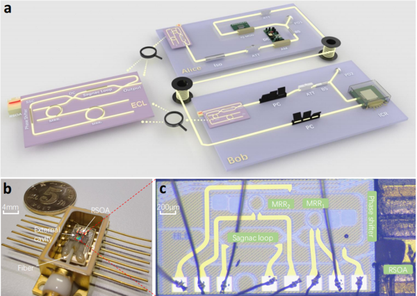
The continuous variable quantum key distribution system (CV-QKD) based on Gaussian modulated coherent state protocol (GMCS protocol, also known as GG02 protocol) has many characteristics such as complete theoretical security proof, high secure key rate, compatibility with existing optical communication architecture, etc. It is one of the promising routes to build a high-performance quantum key distribution network in the future.
Photonics Research
- Jul. 03, 2023
- Vol. 11, Issue 4 (2023)
On the Cover
In optical imaging, "phase" is one of the most important components of the light field (strictly speaking, monochromatic coherent light field). Especially in the field of optical microscopic imaging, most objects are phase objects with weak absorption, where the amplitude of light passing through the object (e.g., a cell) is almost constant, while the phase of transmitted light contains crucial information about the sample, such as 3D morphology and refractive index distribution. The acquisition of phase information is particularly significant, has driven the emergence of "phase measurement" technology. At present, "phase measurement" as a major research direction in the field of optical microscopic imaging, and has been widely applied in the fields of pathology, biological cytology and drug development.
Photonics Research
- Apr. 06, 2023
- Vol. 11, Issue 3 (2023)
On the Cover
Metasurfaces—structured arrays of nanoresonators—are becoming more and more essential in our every-day life. They are already employed in smartphone cameras, are being developed for LiDAR and 3D sensing, and will constitute even more devices in the near future.
Photonics Research
- Mar. 24, 2023
- Vol. 11, Issue 2 (2023)
On the Cover
Bessel beam is a special non-diffractive beam with the unique natures of small central spot and superior self-healing capabilities. In addition, higher-order Bessel beams have the ability of carrying different orbital angular momentum (also known as topological charge). Terahertz wave, which is an electromagnetic wave between microwave and infrared light, have attracted intensive attention in applications of high-speed communication and high-resolution non-destructive imaging due to their ultra-large bandwidth spectrum and extremely low photon energy. Therefore, generating terahertz Bessel beams and flexibly manipulating their characteristics, including order and non-diffraction length, is of great importance to increase communication capacity and improve imaging accuracy.
Photonics Research
- Feb. 09, 2023
- Vol. 11, Issue 1 (2023)
On the Cover
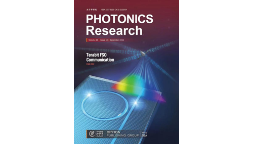
Free-space optical communication (FSOC) uses laser beam as a carrier for information transmission in space. FSOC takes the merits of large communication capacity, anti-electromagnetic interference, good confidentiality, large license-free bandwidths compared with microwave communication system. The communication terminals have the advantages of small volume, easy deployment, and low power consumption, which is an ideal candidate for "last mile" information transmission. It has important application values in emergency, space-to-ground and inter-satellite communications.
Photonics Research
- Dec. 31, 2022
- Vol. 10, Issue 12 (2022)
On the Cover
Metasurfaces have gradually represented powerful abilities to manipulate the amplitude, phase, polarization as well as orbital angular momentum of output light with subwavelength resolution. Due to the subwavelength pixel size, the reconstructed images of metasurface holography can obtain higher resolution and large field of view compare to traditional holography based on spatial light modulator. Meanwhile, the unwanted diffraction orders can also be eliminated.
Photonics Research
- Dec. 07, 2022
- Vol. 10, Issue 11 (2022)
On the Cover
Quantum information science is a new frontier subject combining quantum mechanics and information science. The quantum nature of particle superposition, entanglement, and measurement is applicable for more efficient information processing, computation, transmission, and storage. In the last decades, quantum fundamental science was rapidly transformed into quantum technologies with huge resources invested by global academia, research centers, and industry. Quantum scientific research is moving from the stage of principle verification of quantum rules to the stage of practical device research and development governed by these rules.
Photonics Research
- Nov. 11, 2022
- Vol. 10, Issue 10 (2022)
On the Cover
Single-pixel imaging (SPI) is a novel imaging technique that has been widely studied in recent years. It retrieves spatial information of the target by using a single-pixel detector with no spatial resolution, minimizing the array size of imaging detector, that has unique advantage of making up for the shortcomings of the existing focal plane arrays (FPAs) imaging technology. It is believed that this SPI technology has great application value in special waveband imaging that array detector technology is underdeveloped or expensive.
Photonics Research
- Sep. 30, 2022
- Vol. 10, Issue 9 (2022)
On the Cover
Bound states in the continuum (BICs) enable perfect wave localization and significantly enhance light–matter interactions although systems are optically open. Those trapped modes without the leaky-wave radiation in an open continuum are important in numerous applications, including optical nonlinearity, light emitters, and nano-sensors.
Photonics Research
- Sep. 07, 2022
- Vol. 10, Issue 8 (2022)
On the Cover
Femtosecond laser direct writing (FLDW) provides an important technique for the fabrication of integrated photonic quantum chips, but the produced universal photonic quantum computation chips are still limited to two-qubit logic gates, such as the most commonly used controlled NOT (CNOT) gates encoded by path or polarization. Multiqubit logic gates can be decomposed into the combination of a series of single-qubit and two-qubit logic gates in principle, but the circuits become much more complicated to write.
Photonics Research
- Sep. 01, 2022
- Vol. 10, Issue 7 (2022)
On the Cover
Arbitrary manipulation of multi-dimensional optical field is a development tendency of advanced optical system. Conventional optical elements achieve the specific optical functions based on the gradual phase changes accumulated along the propagation path, which leads to the shortcomings of low degree freedom, large device size, and single functionality, etc. To satisfy the urgent requirements of the high-integrity and lightweight optical system, planar optics components based on geometric phase have become a hot research topic in recent years.
Photonics Research
- Jul. 22, 2022
- Vol. 10, Issue 6 (2022)
On the Cover
Vertical-cavity surface-emitting lasers (VCSELs) have many unique features like circular beam, low power consumption, high modulation speed, and easy fabrication of two-dimensional arrays. Now VCSELs have been widely used in optical interconnects, consumer electronics, 3D sensing, and automotive applications.
Photonics Research
- Jun. 08, 2022
- Vol. 10, Issue 5 (2022)
On the Cover
High efficiency, high brightness, and robust micro or sub-microscale light emitting diodes (LEDs) are essential components of emerging virtual/augmented reality devices and systems as well as future ultrahigh resolution mobile displays. Realization of such ultra-small LEDs can also allow large scale integration of electronic and optoelectronic devices on the same chip.
Photonics Research
- May. 03, 2022
- Vol. 10, Issue 4 (2022)
On the Cover
Metasurfaces has provided a brand new nano-platform for controlling wavefront and intergrating traditional optical device. Metasurfaces have successfully applied in miniaturised optics, including wavefront shaping, asymmetric transmission, holographic displays, optical encryption, nonlinear optics, optical cloaking and so on. Especially, metasurface holography assisted by smart algorithms can conquer the challenges to realize large field of view, target-only diffraction orders and enhancement of information capacity.
Photonics Research
- Mar. 22, 2022
- Vol. 10, Issue 3 (2022)
On the Cover
Driven by cost-effective and massive mature CMOS technology, silicon photonics (SiPh) based on Si-on-insulator (SOI) substrates has made a big success to provide various photonics integrated circuits (PICs) building blocks from individual devices to systems in high-volume manufacturing, including nanowaveguide-based passive components, Si PN junction-based modulators, SiGe detectors, and even laser sources based on III-V/Si heterogeneous integration technique.
Photonics Research
- Feb. 22, 2022
- Vol. 10, Issue 2 (2022)
On the Cover

SiGeSn alloys have attracted considerable attention as a versatile group-IV material system for optoelectronic devices. Compared to the group III-V materials, SiGeSn holds advantages on CMOS compatible, low-cost, large wafer size (8-12 inches), high-volume manufacturing, etc. The direct bandgap GeSn as the gain medium is particularly advantageous for achieving the monolithic integration of laser on Si (Fig. 1). The novel laser solution promises a significant advance in Si photonics, which is extensively applied in applications such as data communication and 3D sensing.
Photonics Research
- Jan. 25, 2022
- Vol. 10, Issue 1 (2022)
On the Cover
Metalens is an ultrathin optical element that can focus light using densely arranged subwavelength structures. Due to its extremely small form factor, it has been considered promising for imaging applications that desire an extreme system size, weight, and power, such as in consumer electronics and remote sensing. However, as a major impediment prohibiting the wide adoption of the metalens technology, the aperture size, and consequently the imaging resolution, of a metalens is often limited by lithography processes that are not scalable.
Photonics Research
- Jan. 10, 2022
- Vol. 9, Issue 12 (2021)
On the Cover
The techniques of high-speed communication and high-resolution display kit are both essential to modern life, as they constitute the foundations of those attractive concepts: Internet of Things, virtual/augmented reality, and metverse. If they are expected to be integrated, being realized simultaneously in one single device in the form of visible light communication (VLC) and micro-LED (μLED) array, it will be thrilling that this new technique would combine the advantages of both, such as avoiding occupying the limited electromagnetic sources, confidentiality, energy saving, and large color gamut, etc.
Photonics Research
- Nov. 26, 2021
- Vol. 9, Issue 11 (2021)
On the Cover

As an important parameter of electromagnetic waves, polarization not only describes the oscillation law of the electric field vector, but is also closely related to the spin angular momentum of the photons (circular polarization). It has extensive research and application value in the fields of optical imaging and quantum communication.
Photonics Research
- Oct. 27, 2021
- Vol. 9, Issue 10 (2021)
On the Cover
Developing new ways to manipulate the transportation of light is very important from both the fundamental science and the technological points of view in photonics. In general, the incident and the refracted beams are on either side of the interface normal. Envisioned by Veselago in the 1960s, negative refraction has received intense research efforts from the photonics community with long-term quests for new scopes and functionality.
Photonics Research
- Sep. 30, 2021
- Vol. 9, Issue 8 (2021)
On the Cover
Quantum effect can be exploited to enhance information processing in many ways. Besides speeding up solving certain problems, quantum computers can also be used to construct novel interactive proof systems (IPS). An IPS usually involves a verifier who wants to solve certain problems and a prover who has infinite computational power and can exchange messages with the verifier.
Photonics Research
- Sep. 24, 2021
- Vol. 9, Issue 9 (2021)
On the Cover
Wave and particle are two fundamental properties of nature. The debate of whether light is a wave or a particle is an ancient problem. For examples, Newton regarded that light is a particle, while Huygens, Thomas Young, Maxwell, etc. believed that light is a wave. After the appearance of quantum theory, people came to realize that light can be a contradictory quantum entity, namely, it can be either a wave or a particle, depending upon the circumstances of the experiments. Such a surprising phenomenon is well-known as the principle of wave-particle duality for light.
Photonics Research
- Aug. 12, 2021
- Vol. 9, Issue 7 (2021)
On the Cover
Miniaturization and integration are inevitable trends in development of modern communication systems. In addition, with increasing of the communication capacity, the independent manipulation of multiple spin beams with controllable energy allocation enables practical applications in multiple-target detection radar system, multiple-input multiple-output (MIMO) communications, and so on.
Photonics Research
- Jun. 29, 2021
- Vol. 9, Issue 6 (2021)
On the Cover
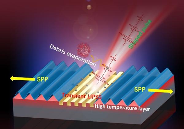
Laser-induced periodic surface structures (LIPSS) provide a direct laser writing method for fabricating nano-gratings on sample surfaces. These periodic nano-structures efficiently modify the properties of materials and have many applications in surface coloring, large-area grating, birefringence optical elements, data storage, and surface wettability.
Photonics Research
- Jun. 01, 2021
- Vol. 9, Issue 5 (2021)
On the Cover
Thermo-optically tunable spectral broadening in a nonlinear ultra-silicon-rich nitride Bragg grating
Optical pulses are essential ingredients in the deployment of imaging systems, precision manufacturing and high-speed communications. The ability to manipulate their properties, including their spectral bandwidth is therefore an important function.
Photonics Research
- Apr. 27, 2021
- Vol. 9, Issue 4 (2021)
On the Cover
Photonics integration is a burgeoning field from both academic and industrial points of view because of its great potentials in aggregating photonic technology with high-performance integrated circuits that may revolutionarily change the architecture of computing. However, many photonics integration platforms suffer from huge challenges in robustness, which make device fabrication, assembling and packaging not compatible with massive production and large-scale integration. To this end, topological concepts are applied and successfully clarified many extraordinary phenomena and further promoted the performance of many devices, as a result, spawn a new branch of modern optics – topological photonics.
Photonics Research
- Apr. 13, 2021
- Vol. 8, Issue 11 (2020)
On the Cover
Optical imaging typically relies on a camera with millions of photodetectors. By contrast, imaging can also take place with a single detector. This is particularly advantageous for imaging at non-visible spectrum where the conventional pixelated cameras lose the sensitivity or become very costly for a good performance.
Photonics Research
- Mar. 31, 2021
- Vol. 9, Issue 3 (2021)
On the Cover
Metasurface-based subtractive color filter fabricated on a 12-inch glass wafer using a CMOS platform
With advanced nanotechnology, the emerging structural color filter which works based on the light-matter interaction is able to overcome the drawbacks of the traditional dye-based color filters including environmental hazards and performance degradation. Therefore, it has been regarded as an essential optical component and widely applied in daily life.
Photonics Research
- Mar. 23, 2021
- Vol. 9, Issue 1 (2021)
On the Cover

Electromagnetic waves with higher spectral purity, frequency stability, and accuracy are consistently pursued in communication, radar systems and global position systems for the goal of large communication capacity and high positioning accuracy. Microwave frequency synthesizers are frequently employed for their generation at any desired frequencies in the microwave region with the same excellent frequency stability and accuracy as those of microwave oscillators or clocks, supporting the variety of applications listed above.
Photonics Research
- Mar. 22, 2021
- Vol. 9, Issue 2 (2021)
On the Cover
High-accuracy long distance ranging plays a significant role in frontier sciences and advanced industrial processing, such as satellite formation flying, spacecraft landing, synthetic aperture radar (SAR), large-scale profile meter, which heavily relies on the precision of a real-time position detection system. During the past decades, laser-based light detection and ranging (LIDAR) takes a major interest in the scientific community for the high angle, distance and velocity resolution, high anti-interference capability.
Photonics Research
- Jan. 14, 2021
- Vol. 8, Issue 12 (2020)
On the Cover
The pursuit of optical-electrics with small size, integration and fast operation requires the efficient control of photon coupling and propagation at nanoscale. The coupling of luminescent medium to optical cavity promotes the directional transmission and reduce the loss of light. Moreover, the confined light can interact with medium.
Photonics Research
- Dec. 02, 2020
- Vol. 8, Issue 11 (2020)
On the Cover

Active sources such as lasers and amplifiers are essential components for photonic integrated circuits (PICs) serving a myriad of applications. Silicon nitride (Si3N4) photonics, due to its low propagation loss (~0.1 dB/cm), wide transparency window (~400 nm to 2.35 µm) and good CMOS compatibility, is found to have increasing number of applications in the fields such as microwave photonics, nonlinear photonics, bio-sensing, and in technology towards autonomous driving like lidar and gyroscopes. In most applications, integration of active components onto the passive Si3N4 platform is required. The integration of III-V semiconductor optical amplifiers (SOA's) and Si3N4 by butt-coupling has led to external cavity lasers of exceptional performance. However, sophisticated assembly and packaging steps with high precision alignment are required, which significantly limits cost-effective scaling of manufacturing.
Photonics Research
- Nov. 04, 2020
- Vol. 8, Issue 10 (2020)
On the Cover
Active imaging over long ranges is of considerable interest in a wide range of applications including remote sensing and target recognition. Single-photon light detection and ranging (LiDAR) presents single-photon sensitivity and picosecond time resolution, which is desirable for long-range imaging. Important progress has been made in the field, and 3D imaging at up to10-km range has been reported. However, further expanding the imaging range presents enormous challenges, because only weak echo photons return and are mixed with strong noise.
Photonics Research
- Nov. 04, 2020
- Vol. 8, Issue 9 (2020)
On the Cover
Smith-Purcell radiation (SPR) is the electromagnetic wave generated by free electrons passing above a diffraction grating, which has played an important role in free electron light sources and particle accelerators. Since SPR is derived from the scattering of the evanescent wave around the free electrons by grating, the characteristics of SPR, including radiation wavelength, intensity, and polarization, could be controlled by manipulating the free electrons and the structure interacting with electrons. In recent years, orbital angular momentum (OAM) has been known as a new degree of freedom of light, which shows promising application in increasing the bandwidth of optical communication, manipulating micro-particles, fabrication of nano-structures, and so on.
Photonics Research
- Sep. 10, 2020
- Vol. 8, Issue 8 (2020)
On the Cover
Airy optical beams have come out to stir up enormous research interests due to their extraordinary characteristics of self-accelerating, self-healing, and being nearly diffraction free. There are various schemes to generate Airy beams, for instance, using spatial light modulators (SLMs). However, they significantly condense the quality of the generated Airy beams due to the poor phase discretization, as Airy beams possessing specific characteristics need phase profiles with large phase slope. Although lately several plasmonic or dielectric metasurface-based generators provide phase profiles with subwavelength pixelization offering a compact and cost-effective platform, the method based on synchronous manipulation of the amplitude and phase limits the generation efficiency of Airy beams. Besides, most of currently demonstrated metasurface-based Airy beam generators are polarization-sensitive.
Photonics Research
- Aug. 07, 2020
- Vol. 8, Issue 7 (2020)
On the Cover
Optical vortex is a special light field with a helical phase front. Due to the helical phase distribution, there is a phase singularity at the center of the vortex field, which causes a point of zero intensity. These unique optical properties make optical vortex show strong application value in many frontier fields including super-resolution imaging, optical manipulation and quantum information technology.
Photonics Research
- Jul. 09, 2020
- Vol. 8, Issue 6 (2020)
On the Cover

As a basic optical element, micro-resonator has been playing an important role in the field of silicon photonics. Ultra-high-Q and compact micro-resonators are recognized as the key for many functional devices for optical filtering, lasering, optical modulation/switching and all-optical photonics. Unfortunately, it is still challenging to realize compact silicon micro-resonators with Q>106 because silicon photonic waveguides fabricated with standard CMOS processes usually have a propagation loss of >1 dB/cm.
Photonics Research
- Jun. 09, 2020
- Vol. 8, Issue 5 (2020)
On the Cover
Inverse design is an attractive and emerging approach to achieve ultra-compact, high-performance, and even new-function integrated silicon photonic devices. Inverse-designed integrated photonic devices can usually have two types of subwavelength structures, "analog" and "digital". For the analog subwavelength photonic device, the cell structure (called "pixel") has a fine size, and the device etched pattern usually has a complex boundary of "arbitrary" bending; its high degree of freedom in inverse design may theoretically achieve high-quality design goals, but the performance of the device is usually greatly affected by fabrication errors. For the digital subwavelength photonic device, the pixel size is generally about an order of magnitude larger, and the device etched pattern has relatively regular rectangular or circular boundaries; the inverse design of digital devices can use simple optimization algorithms to obtain excellent performance and large fabrication tolerance.
Photonics Research
- May. 15, 2020
- Vol. 8, Issue 4 (2020)
On the Cover
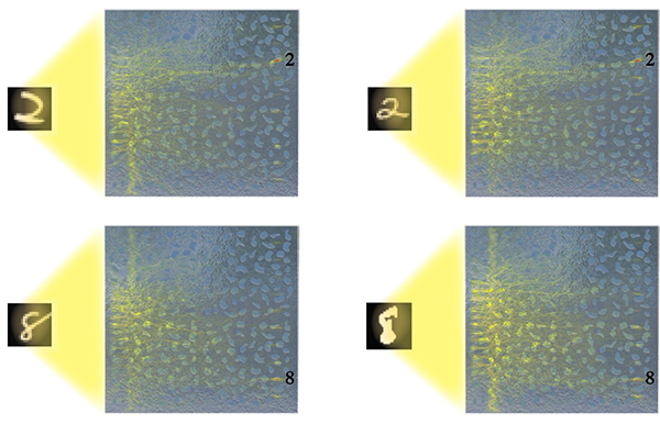
In physics and other science disciplines, it has long been a fundamental issue to make a bridge connecting effectively and efficiently an object in the microscopic world and the observer in the macroscopic world. This is by no means an easy task and it needs great cautions, skills and wisdoms to accomplish.
Photonics Research
- Apr. 16, 2020
- Vol. 8, Issue 3 (2020)
On the Cover
A photonic spin Hall (PSH) device sorts photons with different spin states and is a fundamental component of photonic information technologies. However, the PSH effect is rather weak for measurements using bulky and expensive equipment. The metasurface is a promising way to dramatically shrink an optical element to a size suitable for photonic spin devices. Using V-shaped nano-antennas, a metasurface device with a strong PSH effect is demonstrated with normal incidence. The emergence of a variety of Pancharatnam–Berry phase components has led to development of various photonic spin devices. However, most of these metasurface devices suffer from the low efficiency issues. On-chip photonic spin devices are also designed based on spin-orbital coupling by using micro-disks and nano-antennas, but the intrinsic resonance in this design limits the device’s bandwidth and prevents the wide use.
Photonics Research
- Mar. 24, 2020
- Vol. 8, Issue 2 (2020)
On the Cover
Owing to their ultracompact physical sizes, highly localized coherent output, and efficient waveguiding, one dimensional (1D) components, such as nanowires (NWs), nanotubes, and microwires (MWs), have been considered as one of the most promising building blocks for fully integrated nano/microscale photonic and optoelectronic devices. ZnO has been recognized as a competent candidate for photoelectronic devices because of their excellent inherent electronic and optoelectronic properties. In the study of the research group from Nanjing University of Aeronautics and Astronautics (NUAA), individual ZnO MWs with controlled Ga-doping concentration (ZnO:Ga MWs) were successfully prepared in the synthesis process via chemical vapor deposition (CVD) by means of adjusting the Ga2O3 weight ratios in the precursor reaction mixtures, as well as corresponding the sizes of MWs.
Photonics Research
- Mar. 17, 2020
- Vol. 8, Issue 1 (2020)
On the Cover
Terahertz (THz) imaging, benefiting from THz radiation’s capabilities of non-ionizing and penetration of non-conducting materials, serves as a cutting-edge non-destructive evaluation technology. One of the major challenges in photonics is complex amplitude wavefront sensing, the amplitude image indicates the absorption properties, while the phase image reveals the refractive and thickness information, thus simultaneously determining that the amplitude and phase distributions of the wavefront are highly desirable for applications ranging from bioimaging to material characterization. Due to the long wavelength of the THz wave, the imaging resolution is also one of the key considerations for THz applications.
Photonics Research
- Feb. 12, 2020
- Vol. 7, Issue 12 (2019)
On the Cover
Inspired by the discovery of graphene, researchers have developed a family of two-dimensional (2D) layered materials and investigated their unique optoelectronic properties. Molybdenum disulfide (MoS2), as a kind of typical 2D material, has been intensively investigated due to potential applications in novel electrical and optoelectronic devices. However, in spite of great efforts dedicated to 2D MoS2 study from both experiment and theory, the main challenge remained to be addressed is to achieve 2D MoS2 with high quality and large area, which is the key point for realization of its commercial application.
Photonics Research
- Oct. 30, 2019
- Vol. 7, Issue 10 (2019)
On the Cover
To confirm the feasibility of the new thin film LN approach, Dr. Lutong Cai and Prof. Gianluca Piazza from the Department of Electrical and Computer Engineering at Carnegie Mellon University carried out the first proof-of-concept work of implementing AO modulation devices in LNOI. This work is published in Photonics Research, Volume 7, No. 9, 2019 (L. Cai, et al., Acousto-optical modulation of thin film lithium niobate waveguide devices).
Photonics Research
- Oct. 11, 2019
- Vol. 7, Issue 9 (2019)
On the Cover
The sophisticated technology that powers face recognition in many modern smartphones someday could receive a high-tech upgrade that sounds-and looks-surprisingly low-tech.
This window to the future is none other than a piece of glass-and University of Wisconsin-Madison engineers have devised a method to create pieces of 'smart' glass that can recognize images without requiring any sensors or circuits or power sources.
Photonics Research
- Aug. 14, 2019
- Vol. 7, Issue 8 (2019)
On the Cover
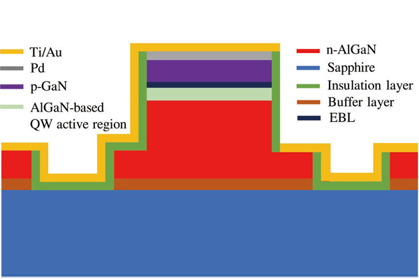
1 Gbps free-space deep ultraviolet communications based on micro-LEDs
Deep Ultraviolet (UV) light with wavelengths below 300 nm is widely used for many different kinds of applications as these short wavelengths can trigger chemical reactions and excite fluorescence in materials. This makes deep UV extremely useful for label tracking, optical sensors, disinfection and decontamination of surfaces and water, curing materials and forensic or drug detection. These applications have driven the development of compact and efficient AlGaN-based deep UV light emitting diodes (LEDs). Another intriguing application is deep UV free-space optical communications, the potential of which has been known for some time, as the properties of light at these short wavelengths can enable unique embodiments of this technology. For example, as most of solar deep UV radiation is absorbed by the ozone layer in Earth's stratosphere, deep UV provides the opportunity to establish high-security free-space optical communication links between satellites in the upper atmosphere where the atmosphere "shields" the communication links from attempts at eavesdropping. Furthermore, since deep UV is strongly scattered in air, a low background noise non-line-of-sight (NLOS) optical communication link with low pointing, acquisition and tracking requirements can be constructed using deep UV light sources on the ground. As a result, it is possible to build a multi-access NLOS optical communication link by using deep UV transmitters. While deep UV communication links have been reported, their performance has been severely limited by the low efficiency and/or modulation bandwidth of the light sources, being either flash tubes, lamps or conventional deep UV LEDs. Therefore, developing deep UV light sources with high modulation bandwidth is of paramount importance.
In recent years, micro-LEDs (μLEDs) have been developed as novel transmitters for visible light based free-space optical communications. These μLEDs, which have lateral dimensions of less than 100 μm, have extremely high modulation bandwidths (in excess of 800 MHz has been reported) which is enabled by their small feature size, which in turn supports very high wireless data transmission rates. It is well known that the modulation bandwidth of LEDs is determined by two factors, namely the resistance-capacitance (RC) time constant and the differential carrier lifetime. For conventional LEDs, the modulation bandwidth is mainly dominated by a large RC time constant due to the large area of the LEDs. As a result, the modulation bandwidth of conventional LEDs is relatively low, typically on the order of 10 MHz. However, in contrast, the modulation bandwidth of μLEDs is mainly dominated by their differential carrier lifetime, thanks to their small area. This carrier lifetime is the average time for electrical charge carriers take to recombine inside the µLED's active region and emit light. The shorter the lifetime, the more rapidly the µLED's optical output can respond to a fast electrical signal and therefore the higher the device's modulation bandwidth. The small feature size of μLEDs allows them to be driven at very high current densities which, since the carrier lifetime generally decreases at higher current densities, means that the modulation bandwidth of μLEDs can be an order of magnitude higher than that of conventional LEDs. These novel characteristics make μLEDs strong transmitter candidates for high-speed free-space optical communications. For example, a data transmission rate over 10 Gbps at a free-space transmission distance of 5 m was recently demonstrated using a series-biased μLED as a transmitter in a visible light free-space optical communication system. It is expected that the µLED device format can also be used to achieve high modulation bandwidths at deep UV wavelengths.
The researchers from the Institute of Photonics, University of Strathclyde and Li-Fi R&D Centre, University of Edinburgh have investigated the modulation characteristics of μLEDs emitting in the UV-C region (200-280 nm) and their applications as light sources in deep UV free-space optical communications. The research results are published in Photonics Research, Volume 7, No. 7, 2019 (X. He, et al., 1 Gbps free-space deep-ultraviolet communications based on III-nitride micro-LEDs emitting at 262 nm).
The deep UV μLEDs fabricated in this work present a great improvement in the modulation bandwidth, which is around 3 times higher than the previously reported modulation bandwidths of other UV-C LEDs. Moreover, at low current densities, the measured modulation bandwidth of the deep UV μLEDs is much higher than that of visible μLEDs, which illustrates the huge potential of the deep UV μLEDs for high-speed free-space optical communications. By applying these deep UV μLEDs into a free-space optical communication link, the data transmission rate is significantly increased, which is more than 15 times higher than the previously reported deep UV optical wireless links. Moreover, the measured modulation bandwidths of the deep UV μLEDs and system data transmission rates are limited by the cut-off frequency of the avalanche photodiode (APD) detector used for the measurement. The researchers consider that an even higher modulation bandwidth of the deep UV μLEDs and, in turn, an even higher deep UV data transmission rate will be achieved if a higher modulation bandwidth APD detector can be applied.
This work presented the excellent modulation performance of the deep UV μLEDs. Moreover, the application of these μLEDs in deep UV high-speed free-space optical communications has also been demonstrated. Future work will focus on the further optimizations of the deep UV μLEDs and optical set up in order to fully explore and realize the potential of these deep UV μLED transmitters. Recently, by adjusting the optical set up and using a high modulation bandwidth APD detector, a deep UV data transmission rate over 3 Gbps is achieved at a free-space transmission distance of 1 m. Furthermore, a NLOS communication link based on the deep UV μLEDs will be constructed in the future.
Cross-sectional schematic diagram of a single deep-ultraviolet μLED
Photonics Research
- Aug. 13, 2019
- Vol. 7, Issue 7 (2019)
On the Cover
The device introduced by Dr. Henri Partanen from a research group from the University of Eastern Finland in Photonics Research, Volume 7, Issue 6, 2019 (H. Partanen, et al., Spectral measurement of coherence Stokes parameters of random broadband light beams) is a general-purpose device to measure the spectral two-point Stokes parameters of arbitrary broadband light beams. To demonstrate the system a well-defined test source with complicated electromagnetic coherence properties is constructed. This is achieved by modulating a uniformly linearly polarized, spatially partially coherent light from a superluminescent diode with a quartz wedge depolarizer leading to a beam with spatially and spectrally varying electromagnetic coherence structure. In order to verify the beam characteristics experimentally we measure the spectral electromagnetic two-point Stokes-parameter distributions, which is achieved in terms of standard, commonly available devices: a double-pinhole interferometer (digital micromirror device), suitable polarization elements (circular polarizers), and a spectrometer (grating). The setup is flexible as the individual components can be chosen for specific situations, e.g., the interferometer can be replaced with a more light-efficient wavefront folding interferometer. As a secondary result, the coherence and polarization variations as a function of wavelength were found to take place at a subnanometer scale.
Photonics Research
- Jul. 08, 2019
- Vol. 7, Issue 6 (2019)
On the Cover

Metasurfaces have enabled rapid development of ultrathin optical devices that can modify the light wavefront by altering its phase and amplitude. Since metasurfaces open a new route to redirect a reflected wave around the object, numerous structures have been put forward to reduce the reflection and scattering of objects, resulting in desired camouflage or invisibility. However, most current phase-gradient metasurfaces are designed in only a single spectrum with narrow bandwidth. Though some dual-band and wideband approaches are achieved by the vertical stacking of metasurfaces, the volume and fabrication difficulty are inevitably increased. In addition, these low-reflection metasurfaces generally cannot achieve thermal invisibility at the same time due to their high infrared absorption/emission arising from the complex metal–dielectric composites.
In order to provide a solution to this challenge, a team of researchers from the State Key Laboratory of Optical Technologies on Nano-Fabrication and Micro-Engineering, Institute of Optics and Electronics, Chinese Academy of Sciences presents a kind of ultrathin silicon-based metasurfaces to simultaneously implement low infrared specular reflection and emission in dual-band and ultra-broadband ranges, respectively. Related research results are published in Photonics Research, Vol. 7, Issue 5, 2019 (Xin Xie, et al.. Dual-band and ultra-broadband photonic spin-orbit interaction for electromagnetic shaping based on single-layer silicon metasurfaces).
Both the metasurfaces comprise a monolayer of amorphous silicon gratings with the same geometry but diverse spatial orientations tiled on a metal mirror, which can generate high-efficiency dual-band and ultra-wideband photonic spin-orbit interaction and geometric phase. The first one is designed to suppress the specular reflectances in dual-band of 1.05-1.08 μm and 5-12 μm below 10%. The second one is for an ultra-broadband of 4.6-14 μm. At the same time, the presented structures exhibit low thermal emission due to the low absorption loss of silicon in the infrared spectrum, which can be regarded as an achievement of laser-infrared compatible camouflage.
Dr. Xin Xie from the research team believes that this work provides a new idea for multispectral and multifunctional electromagnetic wave modulation. Further work will focus on how to extend this strategy to tunable metasurfaces to achieve dynamic electromagnetic camouflage.
Single-layer silicon metasurfaces that can achieve high-efficiency dual-spectrum or ultra-broadband photonic spin-orbit interaction and geometric phase modulation.
Photonics Research
- May. 23, 2019
- Vol. 7, Issue 5 (2019)
On the Cover
Micro light-emitting diodes (μLEDs) are promising candidates for the next generation display technology. However, the efficiency of μLEDs decreases as the size shrinks. Additionally, in order to realize monolithic full-color micro-display, the cost of the RGB mass transfer is enormous, and the color conversion efficiency of the quantum dot (QD) color conversion technology still needs to be improved.
In order to enable μLEDs to be mass-produced as soon as possible. A research group, led by Prof. Hao-Chung Kuo from Institute of Electro-Optical Engineering in Taiwan Chiao Tung University and Dr. Tingzhu Wu from Department of Electronic Science in Xiamen University, carried out the study of full-color monolithic hybrid quantum dot nanoring (NR) μLEDs with improved efficiency. The research results are published in Photonics Research, Volume 7, Issue 4, 2019 (S. Huang Chen, et al., Full-color monolithic hybrid quantum dot nanoring micro light-emitting diodes with improved efficiency using atomic layer deposition and nonradiative resonant energy transfer).
This study reports a novel structure which is the hybrid quantum dot NR micro-LED (QD-NR-μLED). NR structures are fabricated on a green LED epitaxial wafer; the color of NR-μLEDs is tuned from green to blue through strain relaxation. Using the technology of atomic layer deposition (ALD), a 1-nm Al2O3 layer is deposited on the sidewall of blue NR-μLEDs, which improves the photoluminescence intensity of blue NR-μLEDs by 143.7%. Coupling with the exposed multiple quantum wells through nonradiative resonant energy transfer (NRET), red QDs are printed to blue NR-μLEDs for a full-color display. To further improve the color purity of the red light, a distributed Bragg reflector is developed to reuse the excitation light.
In this work, the NR structure provides a structural basis for monolithic full-color micro-display. The ALD sidewall passivation technology improves the luminous efficiency of μLEDs. The NRET mechanism improves the color conversion efficiency of red quantum dots. Therefore, Prof. Kuo and Dr. Wu believes that this novel QD-NR-μLEDs can provide a new idea and a new method for the application of full color micro-displays.
Further work will focus on the optimized thickness of ALD layer as well as how to combine QD-NR-μLEDs with a flexible substrate to achieve flexible transparent micro-displays.
Three subpixels of a green μLED, a blue NR-μLED, and a red QD-NR-μLED, with the deposition of a transparent conducting oxide layer and the pn electrodes.
Photonics Research
- Apr. 22, 2019
- Vol. 7, Issue 4 (2019)
On the Cover
Conventional photodiode detectors made of crystalline semiconductor materials may have special requirements on fabrication affecting device integration, and their response wavelengths are limited by bandgaps, thereby causing limitation on many applications. Comparatively, plasmonic hot electron photodetectors are advantageous in these aspects. The desired response waveband can be obtained by employing appropriate materials and the response spectrum can be adjusted with designed plasmonic characteristics. Therefore, such a type of photodetectors has a broad application prospect in the field of integrated photonics. However, plasmonic hot electron photodetectors require the fabrication of nanostructures, mostly relying on electron beam lithography at present. Not only the process cost is high, but also large-area fabrication is challenging.
In order to provide a solution to this challenge, a nanocone array template is formed on a silica substrate by plasma etching using a monolayer polystyrene nanosphere mask. Metal-semiconductor-metal films are successively deposited on the template, forming an MSM structure for photodetector devices. This work is carried out by Prof. Ting Mei’s group from the Shaanxi Key Laboratory of Optical Information Technology, Northwestern Polytechnical University. The related results are published in Photonics Research, Vol. 7, No. 3, 2019 (Zhiqiang Yang, et al., Silica nanocone array as a template for fabricating a plasmon induced hot electron photodetector).
The nanostructures enable surface plasmon excitation by the incident electromagnetic waves, and propagation of surface plasmon polaritons along the Au interface enhances optical absorption in the Au film. Hot electrons are generated due to plasmon decay, and those with energy larger than the Schottky barrier are emitted over the barrier into the TiO2 layer and eventually reach the Al electrode, accomplishing photoelectric conversion. Especially under an external bias, the response of the device increases, and its response peak gradually shifts red, indicating that the tunneling effect of hot electrons increases with increasing bias voltage. The researchers also use finite element simulation and related numerical theory to confirm the experimental results. In this work, costly electron beam lithography is avoided and the size of the device reaches centimeter level, which will be advantageous for the integration of hot electron photodetectors with a vast variety of optoelectronic and microelectronic devices.
Prof. Mei believes that this work not only gives a new fabrication process for plasmonic hot electron devices compatible for low-cost large-scale monolithic integration, but also provides theoretical guidance on the excitation and transport processes of hot electrons.
Further work will focus on studying nanostructures with stronger plasmon resonance on the basis of which to increase the optical absorption in metal and the efficiency of hot electron generation, and to improve the quantum efficiency of the device.
Device architecture of a plasmonic hot electron photodetector based on a silica nanocone template. Hot electrons are excited due to plasmon decay in the Au film and then travel through the TiO2 layer and eventually reach the Al electrode, forming photocurrent.
Photonics Research
- Mar. 12, 2019
- Vol. 7, Issue 3 (2019)
On the Cover
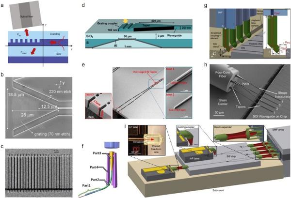
Silicon photonics has rapidly emerged as one of the most prominent technological platforms for the implementation of integrated optical devices. Its compatibility with standard complementary metal-oxide-semiconductor transistor (CMOS) fabrication processes, has enabled low-cost and high-volume manufacturing, making silicon photonics suitable for the implementation of high bit-rate transceivers for data-centre and direct-detection scheme applications. At the same time, silicon photonics technology has been in the forefront for the realization of a number of integrated components for various applications ranging from sensors to microfluidics.
Historically, one of the biggest challenges in designing silicon photonic components, has been related to the realization of high-performance mode converters which can efficiently transfer the light from a standard optical fibre to the integrated circuits. Indeed, this task is particularly challenging due to the strong intrinsic birefringence of integrated silicon waveguides, and to the large size mismatch existing between the optical mode of silicon waveguides and that of single mode fibres (which is almost 800 times larger).
To overcome this issue, the scientific community has proposed different solutions over the last 20 years, which can be schematically divided into two main categories: “end-fire” and “vertical” coupling techniques. In “end-fire” configurations the optical coupling takes place at the edge of the chip in a direction parallel to the chip surface thanks to spot size converters; conversely “vertical” coupling occurs when the incoming beam impinges on the silicon chip almost perpendicularly to its surface and takes advantage of diffractive grating couplers to re-direct the incoming radiations.
Both coupling strategies have different strengths and weaknesses, in terms of performance and ease of fabrication, and can in turn be divided into many different sub-categories, according to the specific design approach employed, and to the chosen materials and fabrication technology.
The group led by Dr. Cosimo Lacava from the Optoelectronics Research Centre, University of Southampton, provides a comprehensive scientific description and view of the various possible solutions that researchers have produced over the last years. They provide the reader with an exhaustive analysis of more than 70 structures reported in the literature, characterized by different level of design and fabrication complexity.
In the review they first describe the physical phenomena underlying the optical coupling mechanism; then they analyze the different coupling solutions available, in terms of their performance (such as coupling efficiency, bandwidth, polarization sensitivity and alignment tolerances) and their compatibility with standard CMOS process flows and packaging techniques. For the benefit of the reader, they benchmark the various coupling solutions against each other in a table at the end, providing the reader with a useful reference, without the need to scan the entire review. This work is published in Photonics Research, Volume 7, Issue 2, 2019 (Riccardo Marchetti, et al., Coupling strategies for silicon photonics integrated chips).
Dr. Cosimo Lacava comments on this work: “The ability to couple a light beam from a SM-fibre to a nanophotonic circuit has always represented a significant challenge for researches working in this field. Although the wording of the problem is simple (How we squeeze the light into a waveguide, which is 800 times smaller than an optical fibre without losing too much energy?), the physics involved is intriguing and technologically complex, and has inspired many scientists who have developed a number of elegant solutions over the years. If you are starting your career as silicon photonic engineer or simply you are looking at the various solutions available to couple the light to your designed integrated circuit, here we provide a comprehensive reference, containing the most common techniques and solutions to accomplish this basic task, vital for the realization of any modern integrated component.”
They believe that future work in the field will be focused on the development of even more efficient coupling structures, where the effort to reduce the couplers insertion loss will have to cope with the necessity to attain full CMOS compatibility and reduction of assembly time and cost, in the perspective of mass-markets manufacturing.
Schematic of a Silicon Photonics circuit. Arrays of angle-polished and planar polished fibres are respectively used to couple the grating- and edge-couplers integrated on the chip. An enlarged schematic of a grating is shown at the top.
Photonics Research
- Mar. 12, 2019
- Vol. 7, Issue 2 (2019)
On the Cover
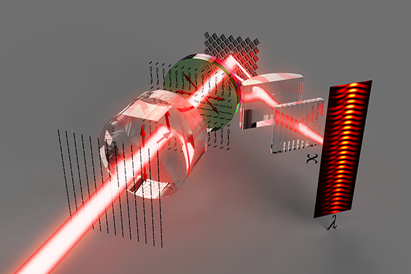
Nonlinear frequency conversion is a crucial technology for operating high power pulsed laser systems at the arbitrary wavelengths required by applications ranging from biological imaging to undersea communications, among many others. A stable and efficient solution based on guided waves, for instance using optical fibers, is in high demand; however, efforts to generate such a device have been limited by the need to conserve momentum, or phase match, in fibers.
Multimode fibers provide the ability to examine nonlinear interactions between guided modes – with the idea multiple modes allow for multiple possible combinations to achieve phase matching. However, in practice, typical intermodal four-wave mixing interactions are only phase-matched over narrow wavelength ranges, leading to impractically narrowband nonlinear gain, inefficiencies in conversion, and limitations in the ability to spectrally and temporally tailor the converted light pulses.
To solve this limitation, the research group from the Nanostructured Fibers and Nonlinear Optics laboratory of Boston University, led by Professor Siddharth Ramachandran, has demonstrated that tailoring of the relative intermodal group velocity, in addition to phase matching, is the key to unlocking extended nonlinear gain bandwidths. This new work highlights an intermodal four-wave mixing process where a pump pulse guided in a superposition of the LP0,4 and LP0,5 modes is converted to two group-velocity-matched pulses in the LP0,4 and LP0,5 modes at wavelengths shorter and longer than that of the pump, respectively. By matching the group velocities of these output pulses, the phase-matched bandwidth is increased by more than order of magnitude compared with typical intermodal processes, leading to broadband gain regions separated by nearly an octave (63 nm centered at 1553 nm, and 17 nm centered at 791 nm). By seeding this process, the authors demonstrate an efficient, quasi-CW, high power and wavelength tunable all-fiber analogue of the ubiquitous Ti:Sapphire laser. This work is published in Photonics Research, Volume 7, Issue 1, 2019 (Jeff Demas, et al., Intermodal group-velocity engineering for broadband nonlinear optics).
In general, these results represent a new parameter space in which to design and implement intermodal parametric nonlinearities – analogous to group velocity dispersion engineering in photonic crystal fibers. Future work will explore using the design flexibility inherent to these multimode systems to target specific wavelength bands for applications underserved by conventional frequency conversion systems, as well as exploiting the bandwidth and group-velocity-matching in these systems to explore fiber-based four-wave mixing in the ultrafast pulse regime.
Schematic of intermodal four-wave mixing: The intense pump pulse (green), guided in a superposition of the LP0,4 and LP0,5 modes (mode image inset), is converted to broadband anti-Stokes (blue) and Stokes (red) pulses along the length of the optical fiber.
Photonics Research
- Mar. 12, 2019
- Vol. 7, Issue 1 (2019)
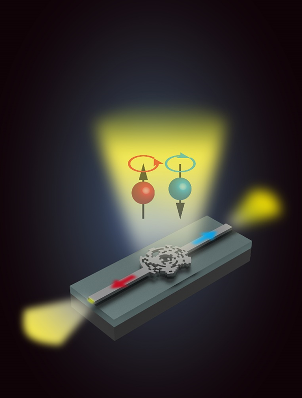
Spotlight on Optics
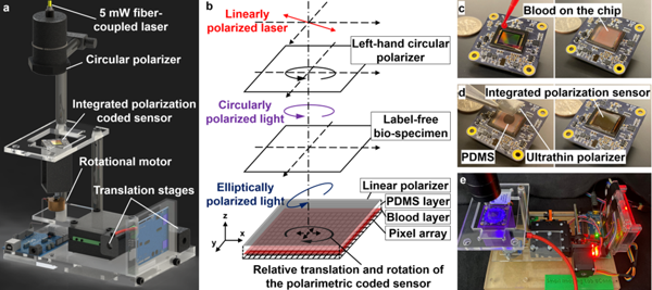
Polarimetric imaging, as a novel optical imaging technique, is widely used in fields such as biomedicine, object recognition, polarimetric remote sensing, and 3D imaging. In the field of biomedicine, polarimetric imaging has two unique advantages compared to traditional optical imaging: 1) By analyzing the polarization properties of light interacting with biospecimens, microscopic-level information about the composition and structure can be obtained without requiring labeling agents. For example, collagen fibers in connective tissues can alter the polarization state of light passing through them. Measuring this alteration provides information about collagen fiber orientation and density, which are associated with various diseases such as cancer and fibrosis. 2) By selectively filtering out light waves with certain polarization states, it is possible to enhance image contrast and improve the visibility of certain structures or components based on the birefringence maps.
Photonics Research
- Apr. 11, 2024
- Vol. 11, Issue 12 (2024)
Spotlight on Optics
Metasurfaces, which consist of tailor-made two-dimensional arrays of resonant structures, are promising for achieving planar and compact optical devices capable of shaping optical waves. Their performance is based on the design of the scattering phase of the individual resonant structures. While a variety of functions, such as optical vortex generation or focusing, have been reported separately, finding designs allowing the integration of multiple functions on a single metasurface is needed. This will further stimulate the development of metasurfaces for practical applications in high-speed data communication.
Photonics Research
- Mar. 19, 2024
- Vol. 11, Issue 3 (2024)
Spotlight on Optics
Optically transparent microwave absorbing metasurfaces have shown great potential and are needed in multiple applications environments containing optical windows such as self-adapting electromagnetic stealth and energy harvesting for satellites or unmanned aerial vehicles, owing to their ability to reduce backscattering electromagnetic (EM) signals while keeping continuous optical observation. However, most of the above absorbers operate in the passive mode, and it makes the absorption characteristics fixed and limits their applications such as fitting into the varying surroundings.
Photonics Research
- Mar. 08, 2023
- Vol. 11, Issue 1 (2023)
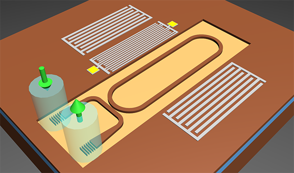
Spotlight on Optics
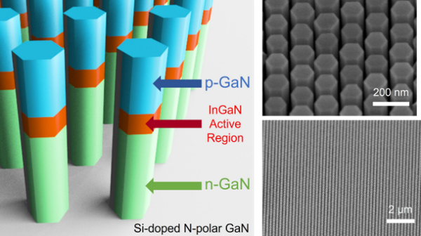
Displays are moving towards higher efficiencies and sharper resolutions with the advent of applications such as augmented and virtual reality. This evolution requires shrinking of the individual pixels that emit light, however it has proven to be quite challenging. Due to their small size, individual devices need to be extremely bright and capable of providing strong luminescence while being self-emitting, which disqualifies existing technologies like organic light emitting diodes (OLEDs) and liquid crystal displays (LCDs). Inorganic semiconductor light emitting diodes (LEDs) can satisfy these requirements, however to date, their efficiency is significantly reduced as the device dimensions are lowered, and this reduction has been primarily attributed to the surface damage induced during LED fabrication.
Photonics Research
- Mar. 03, 2023
- Vol. 10, Issue 12 (2022)
Spotlight on Optics
Visible light communication (VLC) has emerged as a promising communication method in 6G. Compared to traditional wireless communications, VLC operates in the 400–800 THz range, and has different physical features, such as great electromagnetic interference resistance, high confidentiality, and high data rate.
Photonics Research
- Dec. 19, 2022
- Vol. 10, Issue 10 (2022)
Spotlight on Optics
Fast transient events, such as chemical reactions, plasma formation and laser induced damage involve processes that occur at different timescales. Consider for example a plasma assisted reaction event. On the one hand the actual discharge necessitates ultra-high imaging speeds in order to capture its evolution (on the order of THz), while on the other hand, the shockwave induced by the chemical reactions following the plasma pulse moves at a much slower rate.
Photonics Research
- Nov. 21, 2022
- Vol. 10, Issue 7 (2022)
Spotlight on Optics
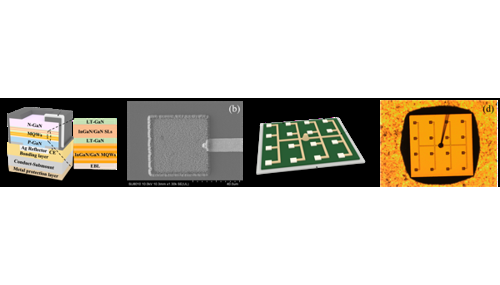
Going beyond human vision capability, infrared can provide objects' important information such as molecular composition and thermal distribution. Because of its characteristics different from visible light, infrared detectors are widely used in night vision, reconnaissance, aerospace, astronomy, weather prediction, health detection, security, environmental monitoring and other scenes.
Photonics Research
- Oct. 20, 2022
- Vol. 10, Issue 8 (2022)
Spotlight on Optics
Optical frequency combs (OFCs) with high frequency resolution and precision have made great progress in the recent decades and innovated the traditional spectral measurement techniques due to the coherently spaced narrow-linewidth comb lines. Recent years, OFCs have been extensively investigated in multiple application fields, such as wavelength division multiplexing (WDM) optical communications, gas sensing and detection, frequency synthesizer and atomic clocks.
Photonics Research
- Sep. 27, 2022
- Vol. 10, Issue 5 (2022)
Spotlight on Optics
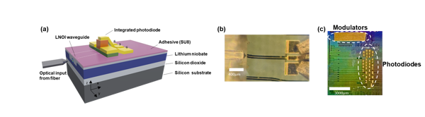
Photonic integration holds the promise for realizing high-performance, low-cost, scalable solutions for communication, sensing, and quantum computation applications. Lithium niobate on insulator (LNOI) is one of the most suitable material platforms for integrated photonic circuits (PICs) due to its unique material properties including the large electro-optic coefficient, the large second-order nonlinear susceptibility, and a wide optical transparency window ranging from the visible to the infrared.
Photonics Research
- Sep. 06, 2022
- Vol. 10, Issue 6 (2022)
Spotlight on Optics
With the development of virtual reality (VR) and augmented reality (AR) technology, the existing display technology is facing challenges and opportunities for providing vivid experience. Among many display technologies, holography shows extraordinary advantages in multi-dimensional optical recording and reconstruction, and is envisioned as the way to the ultimate visual feast.
Photonics Research
- May. 11, 2022
- Vol. 10, Issue 4 (2022)
Spotlight on Optics
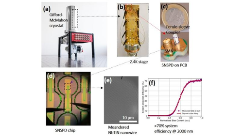
In the past few decades, driven by the development of quantum photonics science and technology, detecting single photons with high efficiency and high accuracy in time has become the essential requirement for many game-changing applications
Photonics Research
- Apr. 24, 2022
- Vol. 10, Issue 4 (2022)
Spotlight on Optics
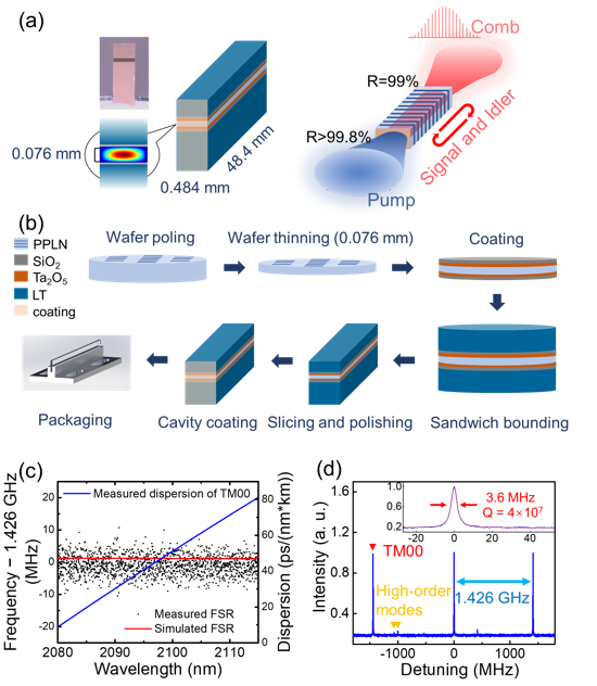
Microresonator-based optical frequency comb (MOFC) integrates the revolutionary comb precision in a small package for practical applications such as spectroscopy, astronomy, microwave photonics and telecommunication. Most of the research on MOFCs uses the third-order nonlinearity (χ(3)) of materials to generate a cascaded four-wave mixing effect near the wavelength of the pump light, which are mainly concentrated in the conventional communication band. While in other important bands such as mid-infrared (MIR) band, it is difficult to generate a such OFC due to the lack of a corresponding high-performance laser as the pump light.
Photonics Research
- Apr. 12, 2022
- Vol. 10, Issue 2 (2022)
Spotlight on Optics
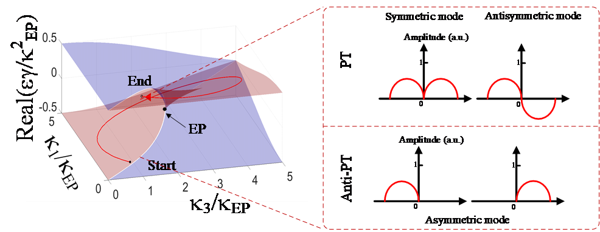
Parity-time (PT) symmetry, as a physical concept, describes the special and temporal symmetry of the physical quantity. Recent year, it has been discovered that PT symmetry can be easily observed in the photonics system. Exceptional point (EP) is a particular point in the PT symmetric system, at which the eigenvalues and eigenvectors degenerate. Plenty of counterintuitive phenomena have been observed around EP. Specially, owing to the non-Hermiticity induced nonadiabatic transitions, chiral mode switching was achieved by encircling the exceptional point (EEP) in a PT symmetric system.
Photonics Research
- Jan. 21, 2022
- Vol. 10, Issue 1 (2022)
Spotlight on Optics
Optics in free space is a long-established, traditional branch of optics. One might expect only incremental advances in this field by now. Actually, nothing could be further from the truth. In a world where devices are ever more connected, exchanging massive amounts of data, free-space optics (FSO) is being deeply reconsidered, and is returning to the leading edge of optics research.
Photonics Research
- Jan. 14, 2022
- Vol. 9, Issue 11 (2021)
Spotlight on Optics
Widely frequency tunable, ultrafast laser sources are utilized in applications such as coherent anti-Stokes Raman spectroscopy (CARS), multiphoton microscopy, frequency combs and terahertz generation. Moreover, they are a unique opportunity to reach wavelength ranges which are not accessible by typical laser gain media due to their utilization of real energy levels for amplification.
Photonics Research
- Nov. 02, 2021
- Vol. 9, Issue 9 (2021)
Spotlight on Optics
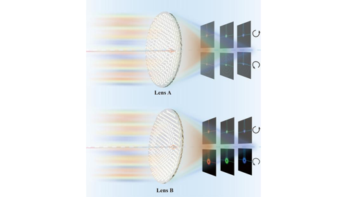
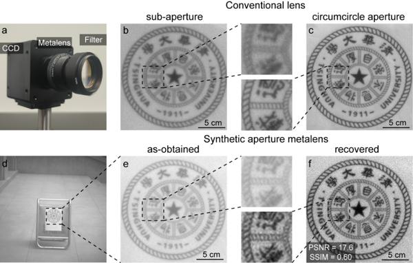
Chromatic aberration of an optical lens arises from the variation of focal length with respect to the wavelength of light caused by the material dispersion, which is a common phenomenon in white light imaging. This aberration will lead to the color blurring and severely degrade the image quality.
Photonics Research
- Sep. 15, 2021
- Vol. 9, Issue 7 (2021)
Spotlight on Optics
A new round of scientific and technological revolution is on-going around the world, Internet technology and smart terminals are constantly developing. Especially after the outbreak of COVID-19 in 2020, emerging businesses such as online education, online office, and online medical services have developed rapidly. The role of the Internet as an infrastructure to support the development of human society has become increasingly prominent.
Photonics Research
- Jul. 01, 2021
- Vol. 9, Issue 5 (2021)
Spotlight on Optics
Understanding matter—a collection of many interacting constituents, such as atoms and electrons, which is a major endeavor in physics. Discoveries of topological insulator and quantum Hall effect have boosted the exploration of novel topological phases of matters. It provides both fascinating physics and exciting opportunities for devices.
Photonics Research
- Apr. 22, 2021
- Vol. 9, Issue 1 (2021)
Spotlight on Optics
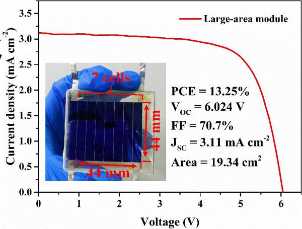
Organic solar cells (OSCs) have many advantages such as low cost, light weight, and flexibility. They have broad prospects and have become one of the most important directions in photovoltaic technologies. Large-area fabrication of organic photovoltaic modules (OPMs) is the key technique to realizing the commercialization of organic photovoltaics. Therefore, it has great practical significance to develop the high-performance large-area OPMs.
Photonics Research
- Apr. 14, 2021
- Vol. 9, Issue 3 (2021)
Spotlight on Optics
Optical fiber is the most broadly used optical waveguide for transmitting light because of its low loss transmission even over long distances and its flexibility, which has been used for illumination and collection of light in various applications including optical fiber biosensors and chemical sensors, fiber lasers, and in-fiber near-field imaging. With the increasing demand for nanoscale photonic devices and quantum communication, an efficient way is needed to focus the light transmitted by optical fiber (the photonic mode) down to nanoscale-confined light. Surface plasmon polariton (SPP) waveguides can control and confine light in the nanometer scale as the light is propagating along the metal-dielectric interface. However, the travel distance of SPP is in the micrometer scale due to the high optical loss. Thus, efficient coupling of low-loss photonic waveguide modes to the highly-confined SPP mode and vice versa is necessary for practical nanoscale fiber optics. The development of these optical fiber nanofocusing devices has been challenging as it requires the phase matching of photonic mode and plasmonic mode that exhibit different mode sizes (microscale vs nanoscale) and mode profiles (with the plasmonic mode being naturally radially polarized). Additionally, current attempts to integrate a nanometer-sized plasmonic nano-waveguide, e.g. a metal nanowire, onto a micrometer-sized fiber have required a challenging fabrication process with multiple procedures and precise alignments.
Photonics Research
- Apr. 08, 2021
- Vol. 9, Issue 2 (2021)
Spotlight on Optics
Silicon based integrated optical circuit can confine the light field in sub-micron scale, and the fabrication process is compatible with mature microelectronic CMOS process. It can realize large-scale, high-density and low-cost on-chip photonic integration, which has become a hot direction of academic research and industrial applications.
Photonics Research
- Feb. 02, 2021
- Vol. 8, Issue 12 (2020)
Spotlight on Optics
Optical frequency combs (OFCs) consisting of equally spaced discrete optical frequency components have emerged as promising tools for a wide range of applications including metrology, optical communications, optical clock distribution/recovery, radio-over-fibre signal generation and optical sampling. Among all approaches for OFCs generations, semiconductor mode-locked lasers (MLLs), motivated by its ability to generate stable and cost-effective high-repetition-rate optical pulses with extremely simple structures, are being heavily investigated as light sources in optical-communications systems. Moreover, an MLL typically provides 5-10 nm bandwidth, promising comb-based transmitters.
Photonics Research
- Jan. 04, 2021
- Vol. 8, Issue 12 (2020)
Spotlight on Optics
Lead halide perovskites have drawn extensive attention over recent decades owing to their advantages of high absorption coefficient, large carrier diffusion lengths, and superior photoelectric properties, which make them as promising candidates for solar cells, light-emitting diodes, photodetectors and lasers. However, their toxicity and instability as big issues need to be solved for further commercialization. So far, many efforts have been made to explore low- or non-toxic elements to replace lead, including tin (Sn), bismuth (Bi), silver (Ag), indium (In), antimony (Sb), germanium (Ge), and copper (Cu). Among these rising lead-free perovskite materials, all inorganic copper-based perovskites benefit from low cost and earth-abundant. In the previous reports, a limited number of synthetic methods have been used to fabricate copper based inorganic perovskites, and there are some problems in these methods, such as energy consumption, time consuming and solvent consuming, which is not accord with the concept of environment-friendly development.
Photonics Research
- Jul. 31, 2020
- Vol. 8, Issue 6 (2020)
Spotlight on Optics
The intelligence technology represented by artificial neural networks has brought tremendous changes in various fields. However, the design and training of different artificial neural networks for different target tasks usually involve complex parameter optimization processes. With the continuous growth of the current network scale as well as the confronted bottleneck of Moore's Law, the time cost and energy consumption required for training and implementing artificial neural networks with the electronic computing are dramatically increasing that cannot support the continuous development of artificial intelligence. Optoelectronic computing possesses the advantages of high speed, high parallelism, and low power consumption. Therefore, developing the optical neural networks and its in situ optical training methods based on optoelectronic computing platforms are expected to achieve disruptive improvement in training time, computation speed, and energy efficiency of artificial intelligence systems.
Photonics Research
- Jul. 15, 2020
- Vol. 8, Issue 6 (2020)
Spotlight on Optics
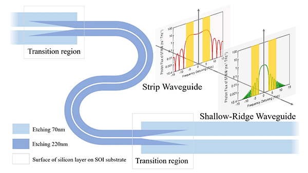
Silicon quantum photonic circuit is an important way to realize the integration of photonic quantum information functions. In telecom band, silicon waveguides have very high third-order optical nonlinear coefficient. They are promising candidates for realizing four-wave mixing (FWM) based quantum light sources operating at room temperature. On the other hand, a variety of silicon photonic devices with different functions provide rich means for on-chip manipulation of photonic quantum states.
Photonics Research
- Apr. 26, 2020
- Vol. 8, Issue 3 (2020)
Spotlight on Optics
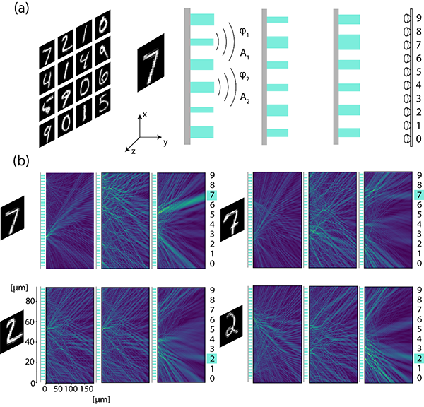
Optical neuromorphic computing offers an alternative approach to realize artificial neural computing. Compared to digital neural computing, it has several potential advantages such as ultra-fast speed and ultra-low energy consumption. In this paper, we introduce a platform to realize artificial neural computing based on metasurfaces (Zhicheng Wu, Ming Zhou, Erfan Khoram, Boyuan Liu, Zongfu Yu. Neuromorphic metasurface[J]. Photonics Research, 2020, 8(1): 01000046). Metasurfaces were developed to perform arbitrary wavefront engineering. Their optical functions are realized by the resonant scattering of nanoscale scatterers. And the scatterers are fabricated on a flat surface. Besides, the metasurface is also compatible with today’s nanofabrication and can be mass-produced at a low cost. Based on the property of metasurface, here, we use it to perform neural computing. In the following, we describe the design procedures and show it utility by the recognition of handwritten digits.
Photonics Research
- Mar. 17, 2020
- Vol. 8, Issue 1 (2020)
Spotlight on Optics

When talking about photonic integrated circuits, one of the first questions we are asked about is their polarization sensitivity. The main reason is that it is extremely challenging to realize photonic devices that are polarization insensitive, especially when we use high-index-contrast platforms like silicon photonics. On the other hand, it is also true that making a device with an ultra-high polarization dependence can be equally difficult. Polarizers should be as transparent as possible to one polarization state while being as lossy as possible to the orthogonal state. However, it’s still a challenge to produce integrated polarizers with a small size, low loss, high polarization selectivity, and operating on a broad band.
Photonics Research
- Feb. 13, 2020
- Vol. 7, Issue 12 (2019)
Editors' Picks
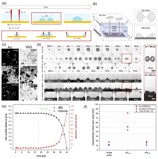
Pulsed Laser Ablation in Liquid (PLAL) is a cutting-edge technique for nanoparticle synthesis. The technique can be understood as the irradiation with a laser source of a material immersed in a liquid. The versatility of the technique due to the possibility to change the liquid and irradiated material represents a critical advantage. Besides, the nanoparticles can also be tailored by adding specific ions and dopants, allowing precise control over the nanoparticles' composition and surface chemistry. This control is essential for catalysis, or nanomedicine applications where purity, composition, and nanoparticle surface groups directly influence the performance.
Photonics Research
- Mar. 14, 2024
- Vol. 11, Issue 12 (2024)
Editors' Picks
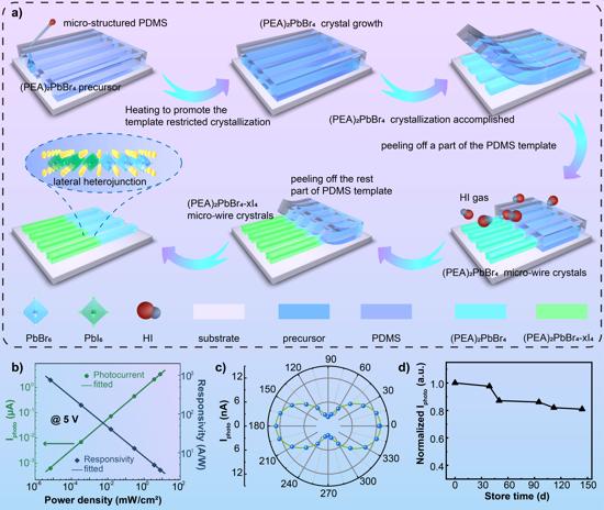
With the continuous expansion of the application of photodetectors in traditional sensing, communication, imaging fields, as well as emerging fields such as flexible robotics and artificial intelligence, the demand for photodetectors is increasing. Particularly, for some new application scenarios, the self-powering capability and sensitivity to polarization information of photodetectors have become increasingly important. However, it is difficult for photodetectors based on single-component active layers to simultaneously meet all these requirements. In contrast, employing carefully designed heterogeneous structures with different optoelectronic properties of materials is a highly effective means to achieve multiple advantages of photodetectors. By composing heterogeneous structures with materials of different optoelectronic performances, the advantages of various materials can be fully utilized, enabling flexibility, self-powering capability, and sensitivity to polarization information in photodetectors. This approach provides new possibilities for the design and performance enhancement of photodetectors, and is expected to further promote their development in various application fields.
Photonics Research
- Mar. 04, 2024
- Vol. 11, Issue 12 (2024)
Editors' Picks
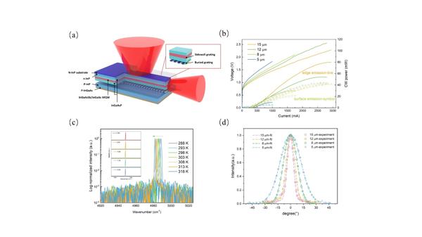
InP-based InGaAs (Sb) quantum well laser is a new type of short-wave mid-infrared semiconductor laser based on interband transition, and its emission wavelength can cover the range of 2 ∼ 3 μm. It has broad application prospects in the fields of trace gas detection and isotope measurement.
Photonics Research
- Feb. 20, 2024
- Vol. 11, Issue 8 (2024)
Editors' Picks
Photodetection in the solar-blind deep ultraviolet (DUV) wavelength region is of central importance in various civil and industrial applications. Recently, the research of solid-state semiconductor DUV photodetectors has attracted much attention, stimulated by the development needs of its small size, energy-saving, and smart detection modules. For solar-blind DUV detection, however, sensitivity below the magnitude of fW is generally required in many key applications, including flame sensing, corona discharge observations, UV astronomy, and biological and chemical agent detection. Although this demand is in line with the current development trend of single-photon detection, it poses a very challenging task for the signal response capability of solid-state DUV detectors.
Photonics Research
- Feb. 20, 2024
- Vol. 11, Issue 7 (2024)
Editors' Picks
The control of light-matter coupling at the single electron level is currently a subject of growing interest for the development of quantum devices and quantum electrodynamics research. In the THz frequency domain, the wavelength in the 100's µm range makes the interaction of light with nanoscale single emitters difficult. THz resonators are used to enhance the light-matter interaction, and it is often desirable to develop resonators that conciliate high quality factors Q, to promote coherent energy exchange between light and matter, with small mode volumes V for the electromagnetic field spatial concentration.
Photonics Research
- Feb. 20, 2024
- Vol. 11, Issue 7 (2024)
Editors' Picks
The dynamic tuning of metamaterials is one of the most attractive research branches in recent years. The functionalities in tunable metamaterials can be controlled under the external stimulus (e.g. electricity, light, magnetism, heat, etc.) and an individual meta-device is empowered with multiple functionalities. The common tunning methods can be divided into two groups, where one is to modulate the electromagnetic responses by manipulating the active constituent elements or materials of metamaterials under the various external conditions, and the other is to utilize the mechanical strategies to change the geometric shapes of metamaterials to tune the responses. The former methods have been widely discussed and investigated by researchers and applied in the dynamic manipulations of amplitudes, polarization states, wavefronts, beam deflection, etc. For morphologically reconfigurable metamaterials, the current research concentrates on the deformation of flexible substrates or kirigami/origami platforms to tune the spectral responses such as chirality, absorption, etc. Also, a few researchers have utilized deformable units to design metalens, in which the focusing length can be enlarged or reduced by changing the periodicity of units during the stretching or the releasing process. Nevertheless, the existing mechanical deformation patterns of reconfigurable metamaterials are still relatively single and the available tuning functionalities are also limited. Therefore, developing novel methods of mechanical deformation can provide possibilities for extending the functionalities reconfigurable metamaterials furtherly.
Photonics Research
- Feb. 01, 2024
- Vol. 11, Issue 10 (2024)
Editors' Picks
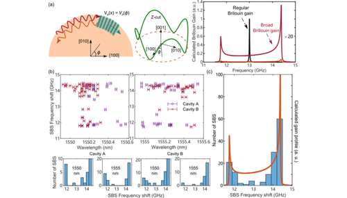
Stimulated Brillouin scattering (SBS) is a nonlinear optical process involving the interaction of light waves with acoustic waves in materials and has important applications in both fundamental science and engineering technology. SBS can be used for low-noise single-frequency lasers, high-sensitivity sensors, signal processing in microwave photonics, optical isolation in optical communication, optical storage, and other signal processing technologies.
Photonics Research
- Jan. 11, 2024
- Vol. 11, Issue 6 (2024)
Editors' Picks
In recent years, artificial intelligence, big data and the Internet of Things have the higher requirements for the speed and efficiency of data processing. However, due to the separation of storage and computing structures, the conventional computing systems have the bottleneck problems in power consumption and efficiency when processing intensive-data and artificial intelligence tasks. The human brain is one of the most complex computing systems, which is capable of storing, integrating and processing a large amount of data and information simultaneously by the densely coordinated synaptic and neural networks. It has the advantages of both high speed and low-power consumption. Inspired by the human brain, artificial synaptic devices have received widespread attention due to their ability to process and remember data simultaneously, which are expected to be the core components in the next generation of neuromorphic computing systems.
Photonics Research
- Dec. 22, 2023
- Vol. 11, Issue 10 (2023)
Editors' Picks
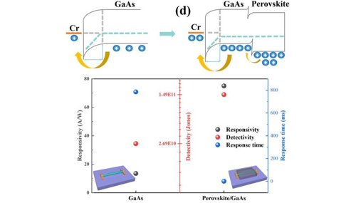
High performance photodetectors are widely used in optical imaging and sensing, environmental monitoring, chemical/biological sensing and other fields, which are of great significance in the military and civilian fields. With the continuous expansion of the application field in recent years, the performance of photoelectric detectors and demand for multi-band detection have increased. Among them, the III-V semiconductor materials represented by GaAs nanowires have been widely studied in the field of photoelectric detection due to their high electron mobility and photoelectric conversion efficiency. Constructing photodetectors with GaAs nanowires is conducive to achieving high-performance multi band detection.
Photonics Research
- Nov. 29, 2023
- Vol. 11, Issue 4 (2023)
Editors' Picks
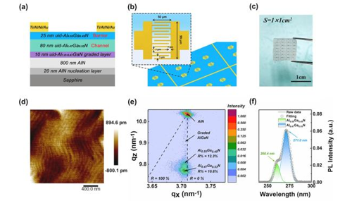
Photodetection in the solar-blind deep ultraviolet (DUV) wavelength region is of central importance in various civil and industrial applications. Recently, the research of solid-state semiconductor DUV photodetectors has attracted much attention, stimulated by the development needs of its small size, energy-saving, and smart detection modules. For solar-blind DUV detection, however, sensitivity below the magnitude of fW is generally required in many key applications, including flame sensing, corona discharge observations, UV astronomy, and biological and chemical agent detection. Although this demand is in line with the current development trend of single-photon detection, it poses a very challenging task for the signal response capability of solid-state DUV detectors.
Photonics Research
- Nov. 06, 2023
- Vol. 11, Issue 7 (2023)
Editors' Picks
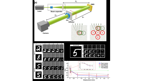
Various scattering media, such as cloud, haze, turbid solution, biological soft tissue, frosted glass, are widely present in nature and daily life. Seeing into and through scattering media has always been a hotspot in research. However, light field propagation in the medium is extremely complex and cannot be accurately described. Despite of the development of a variety of techniques, such as wavefront shaping, optical phase conjugation, scattering matrix measurement, speckle autocorrelation and deconvolution, it still remains at the stage of proof-of-concept with thin scattering media in laboratory.
Photonics Research
- Sep. 21, 2023
- Vol. 11, Issue 6 (2023)
Editors' Picks
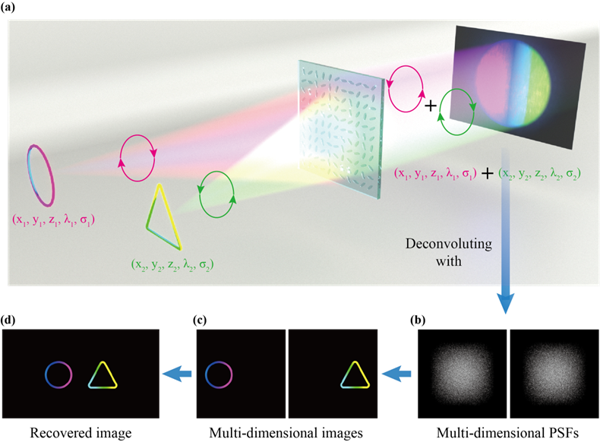
In recent years, with the development of micro-nano optics research, lensless imaging systems based on micro-nano structured diffusers have attracted extensive attention. Unlike the point-to-point imaging method used in traditional imaging systems, the lensless imaging system replaces the traditional lens with diffusers, directly recording the object's encoded pattern on the sensor. The object's information is then recovered through postprocessing algorithms. Due to the lack of a lens, lensless imaging systems have lower manufacturing costs, and can greatly reduce the size and weight of the system, making them suitable for small and portable devices. Recently, using disordered scattering media as imaging lenses or encoding diffusers, significant progress has been made in scattering media imaging, super-resolution imaging and wide-field holography.
Photonics Research
- Sep. 18, 2023
- Vol. 11, Issue 3 (2023)
Editors' Picks
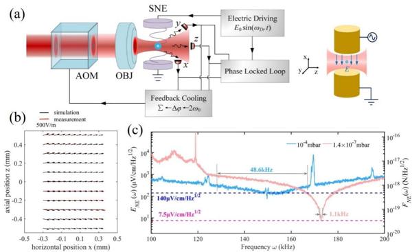
The ability to characterize static and time-dependent electric fields in situ with high sensitivity and high spatial resolution has profound applications for both fundamental science and technology. Precision sensing of electric fields and forces that couple to charge is the most direct way to search for deviations from Coulomb's law, which may be motivated by the presence of new forces under which dark matter could be charged. In addition, low-frequency electric field sensors are widely used in many fields such as geophysical exploration, electrical equipment detection and underwater communication.
Photonics Research
- Sep. 15, 2023
- Vol. 11, Issue 2 (2023)
Editors' Picks
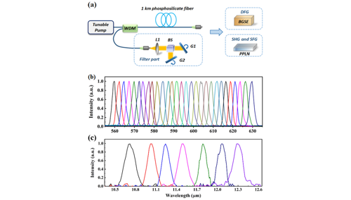
Random fiber lasers (RFLs) can be realized based on the Rayleigh backscattering in fiber as random distributed feedback, without using the fixed resonator in traditional fiber laser. The cavity-free nature of RFLs not only substantially simplifies the constructions of fiber lasers, but also gives RFLs unique merits, such as high brightness, modeless spectrum and ultra-broad wavelength tunability. The wavelengths of cascaded Raman RFLs (RRFLs) have covered 1-2 µm region with high output power, combining with nonlinear frequency conversions, the RFLs are expected to be ideal driving sources for generating visible and mid-infrared light. Moreover, the visible or mid-infrared light generated by frequency conversion of the RFL can inherit the characteristics such as modeless, low noise, low temporal and/or spatial coherence, which could extend the applications of RFLs which require low-coherence light sources such as temporal ghost imaging and speckle-free imaging to different wavelength regions.
Photonics Research
- Jun. 16, 2023
- Vol. 11, Issue 5 (2023)
Editors' Picks
The ability to control the polarization state with high speed is of substantial interest in optical communication systems such as those using high-speed complex digital signal processing (DSP) to manipulate the TE-TM polarization state of light or Stokes vector (SV) modulation and direct detection (SVM/DD) systems. For these applications, there is a growing interest in integrating a polarization controller with the light source, the detectors, and other components in a photonic integrated circuit (PIC). As an increasing number of devices such as laser diodes (LDs) and electro-absorption modulators utilize multiple-quantum-well (MQW) structures as the active region, it is desirable to design a polarization controller compatible with MQW structures. Furthermore, high-speed polarization imaging is a compelling application for material characterization(especially for biomedical studies and clinical applications) and dynamic observation of living cells and biological processes.
Photonics Research
- Jun. 09, 2023
- Vol. 11, Issue 4 (2023)
Editors' Picks
The high-energy pulsed laser with green light band (500-560nm) has great application value in scientific research fields such as earth-moon ranging, underwater detection, biomedicine, industrial processing and so on. At the same time, using green pulsed laser as the fundamental frequency light is the most effective and widespread method to generate ultraviolet and deep ultraviolet laser. At present, the mainstream technology to generate high-energy pulsed green laser is still nonlinear frequency conversion (such as frequency doubling/summing) of near-infrared solid or fiber lasers. Due to its large size and complex maintenance, it is difficult to meet the requirements of many applications requiring miniaturized laser, such as airborne, shipborne, earth-moon and underwater detection. Researchers have been seeking a solution for pulsed green laser with high efficiency, small size and free maintenance.
Photonics Research
- Apr. 07, 2023
- Vol. 11, Issue 3 (2023)
Editors' Picks
High-performance gyroscopes for rotation sensing are of pivotal significance for navigation in many types of air, ground, marine, and space applications. Based on the Sagnac effect, i.e., two counter-propagating waves in a rotating loop accumulate a rotation-dependent phase difference, gyroscopes have been realized in optical and matter-wave systems. The precision of a purely Sagnac gyroscope, which is proportional to the surface area enclosed by the optical path, is theoretically limited by the classical shot-noise limit.
Photonics Research
- Mar. 30, 2023
- Vol. 11, Issue 2 (2023)
Editors' Picks
Bound states in the continuum (BICs) are nonradiative states embedded in the spectra of the radiation continuum. The mechanism of BICs provides efficient ways to engineer the quality factor (Q factor) of resonant modes. Recent demonstrations reveal that metallic metasurfaces can support high-Q plasmonic quasi-BICs offering unprecedented opportunities to achieve giant optical field enhancement. This allows for many applications requiring strong light-matter interaction, such as laser generation, Bose-Einstein condensation, and nonlinear enhancement.
Photonics Research
- Mar. 16, 2023
- Vol. 11, Issue 2 (2023)
Editors' Picks
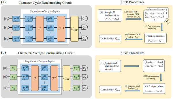
Quantum information science a research field of physics and computer science that studies the fundamental properties of quantum systems and how they can be used in information processing tasks, including quantum cryptography, quantum computing, and quantum metrology.
Photonics Research
- Feb. 23, 2023
- Vol. 11, Issue 1 (2023)
Editors' Picks
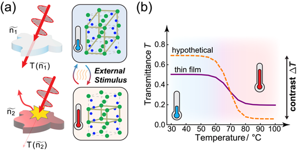
Nanophotonic systems with dynamically tunable properties are of great interest due to their practical applications in optical devices, including power limiters. Among the different tuning mechanisms within the system, one of the most popular is to employ materials that change their refractive index as a result of phase transition. In that regard, vanadium dioxide (VO2) stands out due to the significant index modulation across its insulating-metallic phase transition, which can be triggered thermally or electrically.
Photonics Research
- Feb. 17, 2023
- Vol. 11, Issue 1 (2023)
Editors' Picks
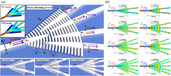
Silicon photonics based on the silicon-on-insulator (SOI) platform, offering a high index-contrast between the silicon core and its surroundings for strong mode field confinement and light-matter interaction, is a promising technology for realizing ultracompact devices in the high-density photonic integrated circuits (PICs).
Photonics Research
- Feb. 09, 2023
- Vol. 10, Issue 11 (2023)
Editors' Picks
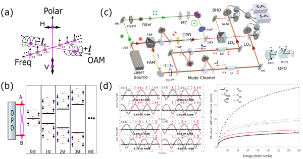
Quantum entanglement plays a pivotal role in quantum information, quantum measurement, quantum communication and quantum computing. The development of entangled state generation and manipulation technologies has greatly promoted the development of the second quantum revolution.
Photonics Research
- Jan. 13, 2023
- Vol. 10, Issue 12 (2023)
Editors' Picks
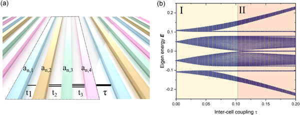
Topological photonics has gained significant interest during the last decade, and holds the unique potential to manipulate light in a disorder-free manner. Different models have been extensively studied to reveal the rich physical mechanisms of topological robust phases and offer diverse applications such as topological lasing and fault-tolerant quantum computing. To describe topological phases, global invariants like the Zak phase and Chern numbers are introduced. In recently years, several measurable methods of quantized Zak phases have been proposed and experimentally demonstrated to characterize topological states in two-band systems, for instance, the celebrated Su-Schrie?er Heeger (SSH) model.
Photonics Research
- Jan. 13, 2023
- Vol. 10, Issue 12 (2023)
Editors' Picks
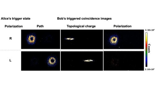
Entanglement is the core resource of quantum information processing. The experimental preparation of entanglement states is a basic task in the field of quantum information. High dimensional quantum entanglement has stronger nonlocality, larger information storage capacity, and better security performance.
Photonics Research
- Jan. 09, 2023
- Vol. 10, Issue 12 (2023)
Editors' Picks
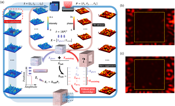
Optical scattering induced information scrambling is one of the biggest challenges that people have to face in optical imaging. Thus, how to overcome the scattering effect and suppress scattering-induced glares is critically important in many scenarios, including deep-tissue optical imaging in biomedical analysis and vehicle perception under the disturbance of rain and fog in daily life.
Photonics Research
- Dec. 31, 2022
- Vol. 10, Issue 12 (2022)
Editors' Picks
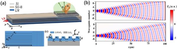
With the rapid development of the information society, information perception technology with high speed, large capacity and low power consumption has become a significant trend of information technology. In particular, optoelectronic integration is expected to be an effective solution for high-performance, low-cost and mass-producible applications in communication and sensing. In the field of laser sensing, Light Detection and Ranging (LiDAR) enables relatively long-range and high-precision 3D imaging, which is critical for future applications in autonomous vehicles, drone detection and long-range machine vision, etc.
Photonics Research
- Dec. 09, 2022
- Vol. 10, Issue 11 (2022)
Editors' Picks
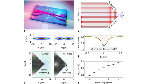
Integrated Fabry-Pérot (FP) cavities are extensively used, finding applications in wavemeters, gravity-wave detection, refractive-index sensing, semiconductor lasers, quantum-information processing, frequency combs, and high-finesse spectral filters.
Photonics Research
- Dec. 07, 2022
- Vol. 10, Issue 11 (2022)
Editors' Picks
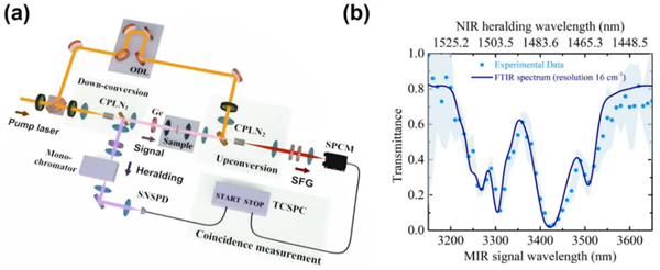
The MIR region (2.5-25 μm) is associated with nature-given properties covering vibrations or rotational transitions of complex molecules. As a result, ultra-sensitive MIR spectroscopy has emerged as an important technique for intelligent biochemical sensing, new materials investigation, environmental gas monitoring, and high-precision medical tomography.
Photonics Research
- Nov. 24, 2022
- Vol. 10, Issue 11 (2022)
Editors' Picks
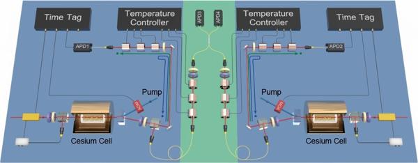
Establishing quantum entanglement between remote nodes is the fundamental primitive for quantum information processing. Due to the increasing photon loss and noise in the channel, quantum repeater scheme is the most promising way to establish the long-distance entanglement, where entanglements are preliminarily generated between intermediate nodes and then extended via linking the adjacent segments by entanglement swapping.
Photonics Research
- Nov. 10, 2022
- Vol. 10, Issue 10 (2022)
Editors' Picks
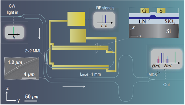
Microwave photonics (MWP) is an emerging interdisciplinary subject which study and utilizes the interplay between light waves and microwaves. It takes advantage of optical devices and systems to perform microwave signal generation, manipulation and transmission tasks. In recent years, the rise of integrated photonics has further promised to build integrated MWP systems that are more compact, integrated and scalable.
Photonics Research
- Oct. 26, 2022
- Vol. 10, Issue 10 (2022)
Editors' Picks
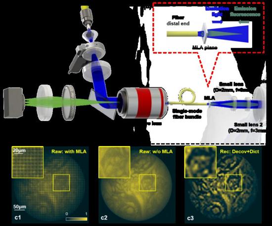
Optical micro-endoscopes are widely used in various biomedical and clinical applications. As a semi-invasive imaging tool, it can detect and image the tissues and viscera of the human body (or other animals), and achieve the visualization of hard-to-reach interior areas. It can also be used to study the brain activities of free-moving animals. In order to reduce the invasive damage, it is usually necessary to limit the size of the endoscopic probe, which will lead to the degradation of imaging performance, especially the axial focusing ability and three-dimensional imaging ability, limiting its important role in disease diagnosis and in vivo observation.
Photonics Research
- Oct. 09, 2022
- Vol. 10, Issue 9 (2022)
Editors' Picks
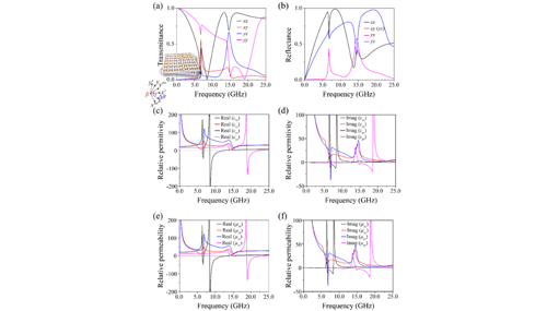
Since the discovery of flat bands and unconventional superconductivity at the magic angle in twisted bilayer graphene by Cao et al., a variety of related exotic phenomena including correlated insulating states and ferromagnetism has been investigated. Analogous twistronic concepts have been extended to phonon and plasmon polaritons in layered low-dimensional photonic materials.
Photonics Research
- Sep. 30, 2022
- Vol. 10, Issue 9 (2022)
Editors' Picks
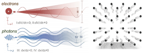
Dynamic localization, originally reported in 1986, refers to the phenomenon that the evolution of electrons is inhibited in the presence of an applied AC electric field. Since 2000, periodically-curved optical waveguides have been used to simulate an external AC electric field, and wave packet suppression has also been observed, and sinusoidal bending waveguides with specific parameters can even completely localize photons in one waveguide.
Photonics Research
- Sep. 27, 2022
- Vol. 10, Issue 6 (2022)
Editors' Picks
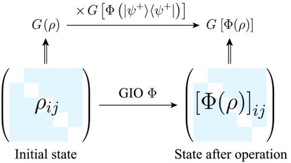
Quantum coherence, which originates from the superposition principle, is an important resource in quantum information processing, showing distinct properties from classical physics. There have been many measures for the degree of coherence of the state of a system. The disturbance of environmental noises leads to the loss of coherence, and thus the quantum advantage.
Photonics Research
- Sep. 26, 2022
- Vol. 10, Issue 9 (2022)
Editors' Picks
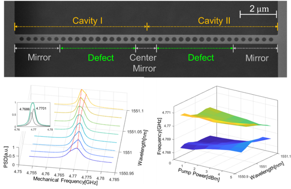
Tunable coupled mechanical resonators have attracted considerable attention in quantum simulations, quantum computations, and non-Hermitian physics. In particular, the tunable coupled mechanical resonators with high mechanical frequency have great potential for realizing high-sensitive exceptional points sensors with increased resistance to environmental disturbances and sensing bandwidth.
Photonics Research
- Sep. 15, 2022
- Vol. 10, Issue 8 (2022)
Editors' Picks
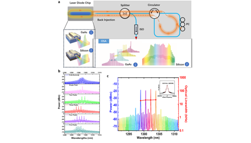
Direct epitaxial grown InAs QD lasers on silicon have attracted significant research attentions with rapid progress over the past decade. But up-to-data, most of researches are based on multi-mode fabry-perot (FP) QD lasers on silicon, which can hardly be implemented in high-performance telecommunications, microwave photonics, and optical interconnects. Therefore, combining direct epitaxially grown InAs QD lasers on silicon with external cavity injection locking becomes trending techniques for generation of narrow-linewidth lasers.
Photonics Research
- Sep. 13, 2022
- Vol. 10, Issue 8 (2022)
Editors' Picks
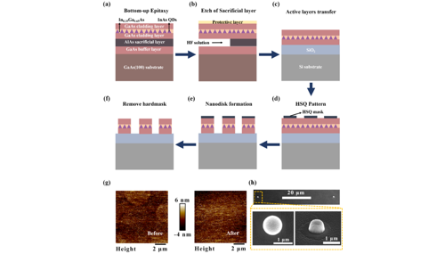
Silicon optical integration technology has the advantages of large bandwidth, low cost, low power consumption, and high integration, which has been widely used in the optical interconnection of telecommunications and data communication. It also has great potential in Lidar and medical sensing and intelligent computing fields. However, as silicon is an indirect bandgap semiconductor, it cannot emit light directly, so silicon-based light source has always been a key problem to be solved in the industry.
Photonics Research
- Aug. 30, 2022
- Vol. 10, Issue 8 (2022)
Editors' Picks
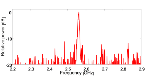
The large-scale integration of electronic devices in silicon circuits has driven the technological revolution of the twentieth century. Over the last two decades, the field of photonics draws great efforts towards similar integration. The huge demand for bandwidth mandates broadband optical communication in ever increasing volumes at the rack, board, and chip levels.
Photonics Research
- Aug. 18, 2022
- Vol. 10, Issue 7 (2022)
Editors' Picks
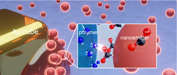
With the rapid development of integrated optics, nanophotonics, quantum optics, etc., the development of nano-light sources with small size, low cost, and stable and controllable performance has become an urgent problem. Hybrid plasmonic nano-emitters as optical nanosources into photonic nanodevices are of interest for research and technological innovation due to their miniaturization and multi-applications. However, how to integrate the emitters near metallic nanostructures with spatial control and nanometer precision in the three space dimensions remains a challenge.
Photonics Research
- Aug. 08, 2022
- Vol. 10, Issue 7 (2022)
Editors' Picks
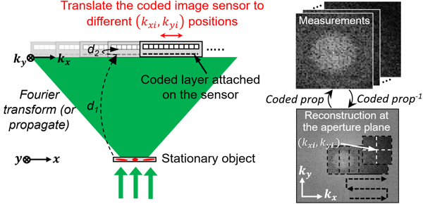
The resolution of a conventional imaging system is limited by the size of the lens. Physically enlarging the lens size leads to a bulky, expensive, and highly specialized optical design. Alternatively, synthetic aperture imaging mitigates the direct coupling between image resolution and lens size. In the radio frequency regime, synthetic aperture radar improves imaging resolution by capturing many images of a static object using a mobile recording platform such as an airplane or satellite. The resolution is no longer limited by the size of the lens antenna. Instead, it is determined by the synthetic aperture size of the mobile recording platform.
Photonics Research
- Jul. 22, 2022
- Vol. 10, Issue 7 (2022)
Editors' Picks
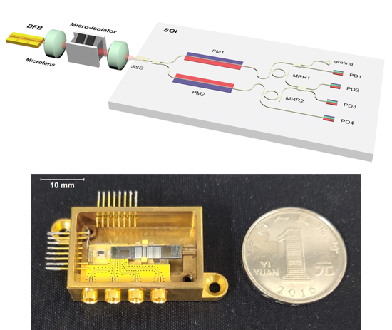
Microwave photonic receivers, featuring the advantages of wide operation bandwidth and flexible reconfigurability, are the promising candidate desired for breaking the bandwidth limitation of traditional RF receivers, which would have broadened applications prospects in global wireless communication, broadband radar systems, and advanced multifunctional RF systems.
Photonics Research
- Jul. 08, 2022
- Vol. 10, Issue 6 (2022)
Editors' Picks
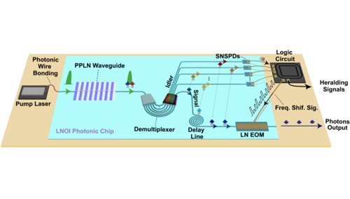
Ideal single photon sources can emit single photons in a pure, deterministic and indistinguishable manner. At present, single-photon sources at telecom-band are widely used in quantum secure communication. They are mainly realized by attenuating laser pulses with randomized phase. However, this kind of single photon source has probabilistic outputs of empty events and multi-photon events, which remains one of the challenges in the application of quantum technology.
Photonics Research
- Jul. 08, 2022
- Vol. 10, Issue 6 (2022)
Editors' Picks
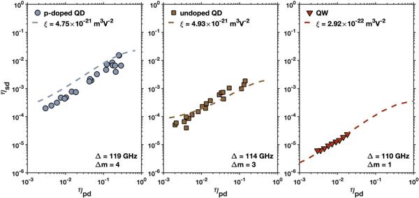
Photonic integrated circuits (PICs) on silicon can significantly advance the level of component integration and performance for both conventional and quantum information processing. The advantages of silicon-based PICs are the availability of manufacturing approaches using modern nanofabrication techniques as well as the potential for miniaturization and integration of optoelectronic components with complementary functionalities.
Photonics Research
- Jun. 30, 2022
- Vol. 10, Issue 5 (2022)
Editors' Picks
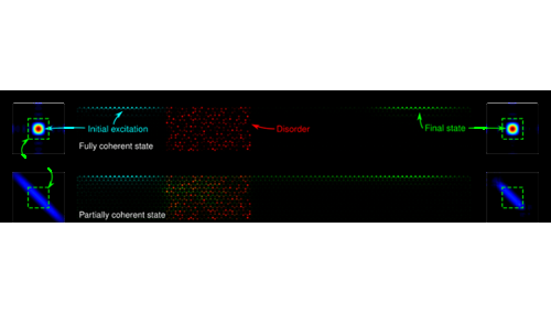
Photonic topological insulators are special materials in whose structural topology fully disallows the energy transport into their interior. Instead, they keep energy circulating along their surfaces. In contrast to ordinary surface wave systems, the prominence of photonic topological insulators lies on the fact that the surface transport occurs in unidirectional fashion, irrespective of whether the system exhibits disorder or contains random imperfections.
Photonics Research
- Jun. 23, 2022
- Vol. 10, Issue 5 (2022)
Editors' Picks
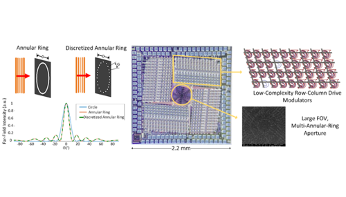
Almost all optical systems, including LiDAR for autonomous vehicles and robotic applications, medical imaging systems such as optical coherent tomography, and high-speed point-to-point optical communication links greatly benefit from a photonic beamforming and beam steering sub-system. This sub-system directs and concentrates the optical beam in the desired direction, improving the system's sensitivity and imaging resolution.
Photonics Research
- Jun. 09, 2022
- Vol. 10, Issue 5 (2022)
Editors' Picks
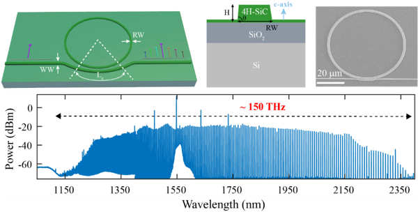
Optical frequency combs have changed science and technology as we know it. They are the enabler of applications including frequency generation and synthesis, image and sensing, light detection and ranging, parallel optical communication and computation, and quantum information processing. Given the importance, half of the 2005 Nobel Physics Prize was awarded to the two inventors of the optical comb technology: John L. Hall and Theodor W. Hansch.
Photonics Research
- Apr. 24, 2022
- Vol. 10, Issue 4 (2022)
Editors' Picks
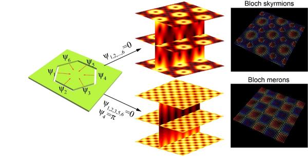
Topological photonics mainly focuses on studying the property of waves in periodic structures such as photonic crystals or metamaterials, by investigating their topological band structures in momentum space. In real space, however, there exists also a variety of fascinating topological phenomena, e. g., optical vortices, optical Möbius strips, and optical skyrmions.
Photonics Research
- Apr. 19, 2022
- Vol. 10, Issue 4 (2022)
Editors' Picks
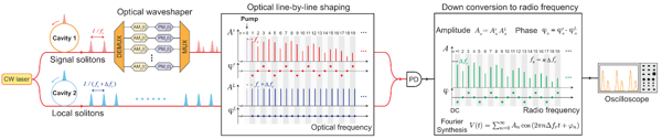
Radio-frequency (RF) waveform synthesis enables wide applications in wireless communications, radar systems, and electronic frequency-domain and time-domain testing.
Photonics Research
- Apr. 15, 2022
- Vol. 10, Issue 4 (2022)
Editors' Picks
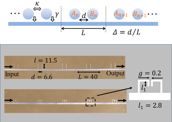
Topological states of matter are one of the most important research fields in condensed physics and have been deeply studied over the last 10 years. Before the discovery of topological states, researchers believed that almost all states of matter could be characterized by symmetry or local order parameters, and the phase transition of matters was accompanied by symmetry breaking.
Photonics Research
- Apr. 08, 2022
- Vol. 10, Issue 1 (2022)
Editors' Picks

Right after the invention of the laser, nonlinear optical effects were observed, with the first demonstration of second harmonic generation in 1961. This field opened fascinating and boundless new possibilities in optics. Research in nonlinear optics then grew and caught the attention of many scientists who discovered and studied new ways to play with light. In parallel, integrated optics rapidly demonstrated its capability to develop efficient and compact devices.
Photonics Research
- Mar. 31, 2022
- Vol. 10, Issue 3 (2022)
Editors' Picks
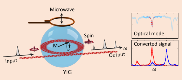
Coherent conversion of microwave and optical photons can significantly expand the capabilities of information processing and communications systems. However, the quantum information technology based on the most promising superconducting qubits is operated at cryogenic temperature with microwave photons, which cannot achieve long-distance communications between qubits.
Photonics Research
- Mar. 31, 2022
- Vol. 10, Issue 3 (2022)
Editors' Picks
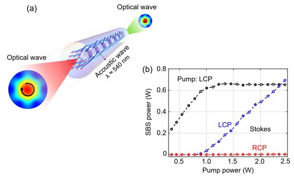
The behaviour of light in chiral structures continues to be a subject of great fundamental interest and many applications are emerging in the various subfields of photonics, such as optical activity in biological molecules, lasing in cholesteric liquid crystals, chiral metamaterials, multielement helical structures that act like topological insulators and chiral photonic crystal fibers (PCF).
Photonics Research
- Mar. 21, 2022
- Vol. 10, Issue 3 (2022)
Editors' Picks
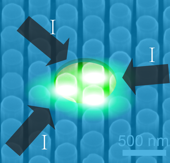
Higher brightness, longer lifetime, higher resolution and better color rendering are being pursued for the next generation display technology that could support the development of virtual/augmented reality and metauniverse. Micro-LEDs are considered as the most promising route to meeting these requirements. Besides display applications, visible light communications, bioimaging and detection are also potential applications of micro-LEDs.
Photonics Research
- Mar. 09, 2022
- Vol. 10, Issue 2 (2022)
Editors' Picks
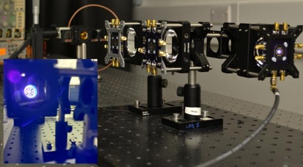
Optical wireless communication (OWC) is emerging as a key technology that can complement radio-frequency (RF) based communication systems, adding hundreds of THz of licence-free bandwidth. Standard visible-wavelength light-emitting diodes (LEDs), mostly based on gallium nitride technology, can support Gigabit per second (Gbps) wireless data rates which can be deployed in lighting-compatible systems, supporting the development of LiFi (light fidelity).
Photonics Research
- Feb. 28, 2022
- Vol. 10, Issue 2 (2022)
Editors' Picks
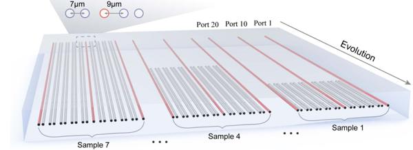
Squeezed light is a key resource for quantum sensing and quantum information processing. Parametric frequency conversion in nonlinear crystals is an indispensable method to obtain non-classical light and generate multi-photon entangled states in quantum optics. Due to the inherent weak optical nonlinearity and limited interaction volume of crystals, considerable pumping power is usually required to obtain effective nonlinear interactions to produce squeezed light, but this often results in undesirable effects, such as damage to nonlinear materials.
Photonics Research
- Feb. 16, 2022
- Vol. 10, Issue 2 (2022)
Editors' Picks
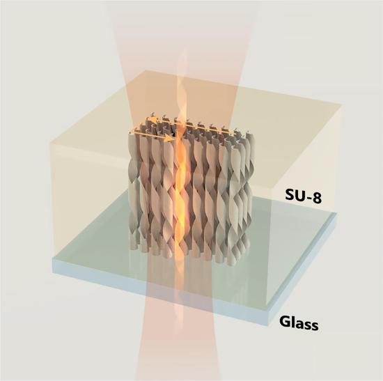
Light, as we know it, travels in a straight line. This also applies to a laser beam which is basically a more intense form of light. Lasers have been used in welding, drilling, cutting, forming and other manufacturing processes ever since they were invented more than 60 years ago. A new generation of lasers has been developed in the past few decades. Commonly referred to as "ultrafast lasers" or "ultrashort-pulsed lasers," this type of laser can output consecutive flashes of light ("pulses") each having very short duration (< 1 picosecond = 10-12 s).
Photonics Research
- Feb. 14, 2022
- Vol. 10, Issue 2 (2022)
Editors' Picks
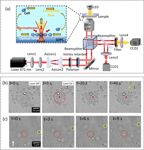
Optical tweezers (OTs) provide a powerful tool for trapping, guiding, and assembly of biological nanoparticles and cells, thus playing a unique role in biomedical and photonics areas. Particularly, OTs have been widely used to explore the structure, mechanism, and interaction of cells due to their ability of non-contact and high-resolution manipulation.
Photonics Research
- Jan. 20, 2022
- Vol. 10, Issue 1 (2022)
Editors' Picks
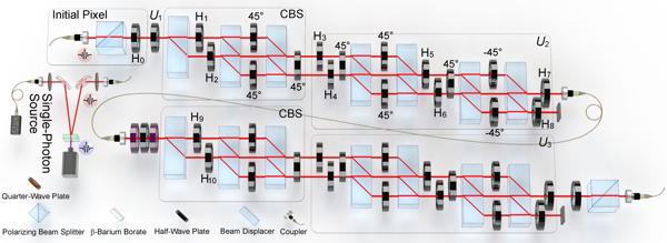
The fundamental principle of machine learning (ML) is the ability of machines to reveal the hidden patterns by learning from existing samples and carry out future work accordingly. The interdisciplinary field of quantum machine learning has seen astonishing progress recently, where novel algorithms presage useful applications for near-term quantum computers.
Photonics Research
- Jan. 17, 2022
- Vol. 9, Issue 12 (2021)
Editors' Picks
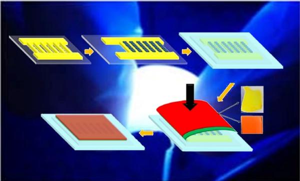
Through technological advances, light-emitting diode (LED)-based systems have been commercialized and are now widely used in applications such as large displays, traffic lights, indoor and street lighting, automobiles, cell phones, and liquid-crystal displays.
Photonics Research
- Jan. 13, 2022
- Vol. 9, Issue 12 (2022)
Editors' Picks
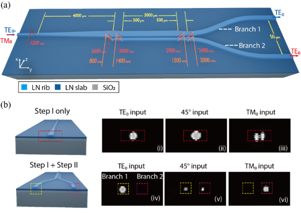
Polarization state of light is one of the most important degrees of freedom for information encoding. Devices that can effectively perform tasks such as polarization rotation and polarization splitting are crucial components for both classical and quantum optical communication systems. In photonic integrated circuits, polarization manipulation devices are also important for processing input optical signals that do not have a pure polarization state.
Photonics Research
- Jan. 12, 2022
- Vol. 9, Issue 12 (2021)
Editors' Picks
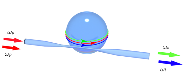
Advances in quantum technologies over the past two decades have made possible an exciting breadth of applications in fields such as communications, and computation. Photon-pair generation based on the spontaneous parametric down conversion and four wave mixing processes have played an essential role in this revolution due to the ease with which the quantum entanglement characteristics of the emitted signal and idler photons may be tailored, and on account of their ability to propagate long distances either in free space or in optical fibers with minimal interaction with the environment.
Photonics Research
- Dec. 03, 2021
- Vol. 9, Issue 11 (2021)
Editors' Picks
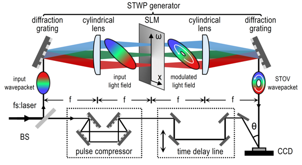
Spatiotemporal (ST) wavepacket has been widely investigated since the invention of ultrafast laser. Conventional research on ST wavepackets focuses on studying spatiotemporal uncoupled wavepacket, meaning the space domain property and time domain property of the wavepacket are exploited separately.
Photonics Research
- Nov. 24, 2021
- Vol. 9, Issue 11 (2021)
Editors' Picks
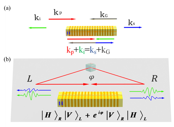
Narrowband photonic entanglement is a crucial resource for long-distance quantum communication and quantum information processing, including quantum memories. However, the entangled photon source needs to be compatible with information processing devices in practical applications, where the photon-electron interaction is normally required. The bandwidth of such photon-electron interaction is fundamentally limited by the energy level of the electrons and often in the order of a hundred megahertz.
Photonics Research
- Nov. 16, 2021
- Vol. 9, Issue 10 (2021)
Editors' Picks
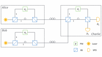
Loading and transmitting information using photons, quantum key distribution can share random key among users with unconditional security. The security is ensured by the quantum nature of photons and independent with computational complexity where any eavesdropping can be detected and quantified. Quantum key distribution has attracted extensive attention, fiber-based quantum key distribution networks using BB84 protocol has been deployed on a large scale, it takes the first step along the roadmap of Quantum Internet.
Photonics Research
- Oct. 25, 2021
- Vol. 9, Issue 10 (2021)
Editors' Picks
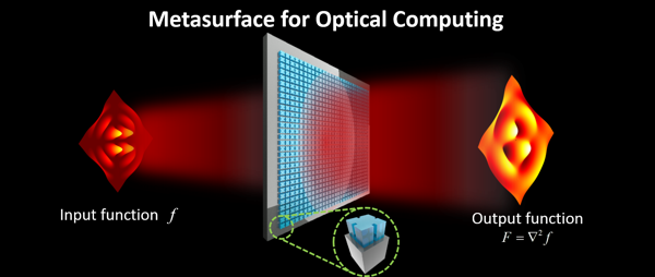
It is an important research topic how to achieve more powerful computing and image-processing abilities, because the processing of huge information and images is in a great demand. In contrast to conventional electronic computers and quantum computers working in a digital way, optical computing working in an analog way is of great potential for parallel computing with low power consumption and high speed.
Photonics Research
- Oct. 08, 2021
- Vol. 9, Issue 9 (2021)
Editors' Picks
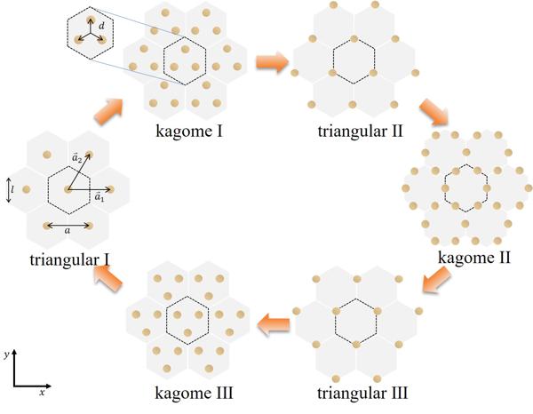
Topological phases and phase transition have been extensively studied in electronic, photonic, and acoustic systems in the past decades. Recently, a new class of topological insulators, called higher-order topological insulators (HOTIs) that are characterized by higher-order bulk-boundary correspondence, were discovered.
Photonics Research
- Sep. 22, 2021
- Vol. 9, Issue 9 (2021)
Editors' Picks
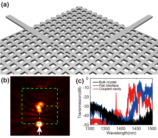
Optical cavity, as one of the important elements of nanophotonics, is widely used in many fields, such as optical communications, sensing, quantum optics, and gravitational-wave detection. These applications have driven the development of high-performance cavity and cavity-based integrated devices, which is highly relevant to the control capability of cavity modes.
Photonics Research
- Sep. 10, 2021
- Vol. 9, Issue 8 (2021)
Editors' Picks
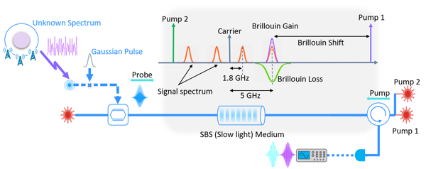
Wireless communication technologies are evolving rapidly to meet the rising demands of high data traffic applications like autonomous driving and the internet-of-things. However, the reach and quality of these new services stand and fall with the bandwidth for the wireless link.
Photonics Research
- Sep. 01, 2021
- Vol. 9, Issue 8 (2021)
Editors' Picks
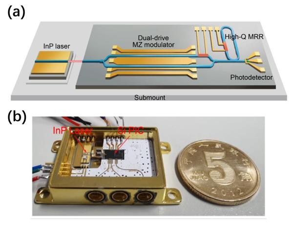
Microwave filters represent a class of devices used to select desired band of RF frequencies, which are widely applied in many fields such as radar, electronic warfare, and wireless communication. Compared to traditional electronic microwave filters, microwave photonic filters (MPFs) operate on signals in optical domain, can offer broad frequency range, excellent tunability and strong immunity to electromagnetic interference.
Photonics Research
- Aug. 24, 2021
- Vol. 9, Issue 8 (2021)
Editors' Picks
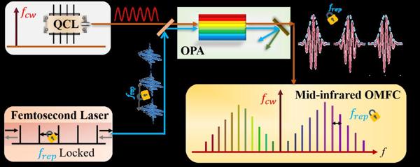
Spectral measurements of molecular fingerprint features are of great significance, which establish the microscopic structures and material compositions. Therefore, a higher request in the measurement resolution, precision, and sensitivity is put forward.
Photonics Research
- Aug. 23, 2021
- Vol. 9, Issue 7 (2021)
Editors' Picks
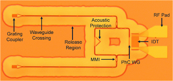
The development of photonic integrated circuit (PIC) applications prompted by optical transceivers for data centers, microwave photonic-based signal processing, quantum computing, spectroscopy, and holography, demands more efficient means to control lightwave propagation. One efficient method to achieve this objective is to utilize light-matter interactions through acousto-optic (AO) devices.
Photonics Research
- Aug. 10, 2021
- Vol. 9, Issue 7 (2021)
Editors' Picks
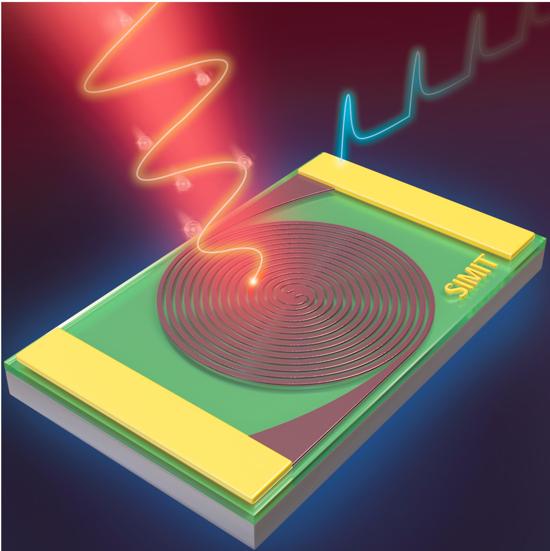
Superconducting single-photon detectors (SSPDs) play a key role in the fields of quantum information processing, quantum optics, deep-space laser communications, and light detection and ranging, owing to high system detection efficiency (SDE), low dark count rate (DCR), low timing jitter (TJ), high photon count rate, and broadband sensitivity.
Photonics Research
- Aug. 05, 2021
- Vol. 9, Issue 6 (2021)
Editors' Picks
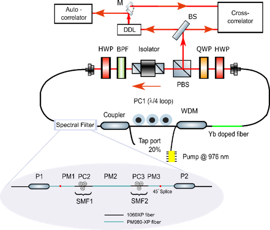
Mode-locked lasers are the building blocks to generate ultrafast pulses which can then be used for many applications, including optical communication, metrology, spectroscopy, microscopy, material processing, as well as many applications in the healthcare industry. Mode-locked fiber lasers are especially popular for their compactness, efficiency, and beam quality compared to their solid-state counterparts. Apart from their practicality, the mode-locked fiber lasers are an interesting object for studies, as they represent dynamically rich nonlinear systems.
Photonics Research
- Jul. 16, 2021
- Vol. 9, Issue 6 (2021)
Editors' Picks
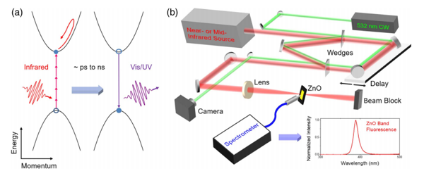
Intense, femtosecond laser pulses have for the last several decades been used for studies of ultrafast dynamics in atomic, molecular, and condensed matter systems. More recently, the development of techniques for nonlinear pulse compression to the single-optical-cycle limit and for stabilizing and controlling the carrier-envelope phase (the phase difference between the peak of the pulse envelope and the closest maximum of the oscillating electric field) has enabled the conversion of intense laser pulses into extreme ultraviolet attosecond pulses and ignited the field of attosecond science.
Photonics Research
- Jul. 09, 2021
- Vol. 9, Issue 6 (2021)
Editors' Picks
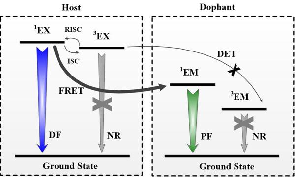
Two-photon excited fluorescence (TPEF) materials can be excited by a near-infrared laser and emit in the visible light band. In view of their high three-dimensional spatial selectivity and superior imaging penetration depth, TPEF materials and technology have charming application prospect in fields of life sciences and medicine.
Photonics Research
- May. 31, 2021
- Vol. 9, Issue 5 (2021)
Editors' Picks
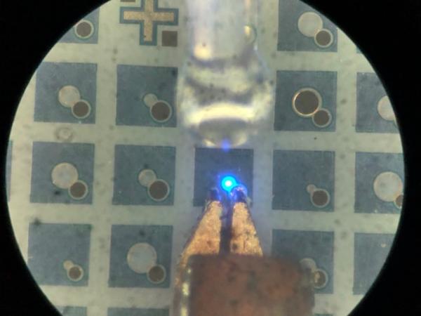
As an important supplement to wireless radio frequency communication in free space and acoustic wave communication in underwater environment, visible light communication (VLC) is considered to be a strong contender for the next generation mobile wireless "last mile" access technology, which has great potential to be widely used in 5G+ or 6G.
Photonics Research
- May. 28, 2021
- Vol. 9, Issue 5 (2021)
Editors' Picks
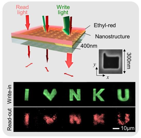
Promoted by enthusiasm for future massive data processing by photons in parallel architectures, spatial light modulators (SLMs) were invented half a century ago. With the help of external control signals, such devices can manipulate light by modulating its amplitude, phase or polarization both spatially and temporally at will, which enables encoding information into an optical wavefront.
Photonics Research
- May. 11, 2021
- Vol. 9, Issue 4 (2021)
Editors' Picks
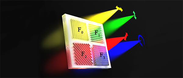
Polarization state, as one of the important properties of light, is widely used in many fields, such as satellite remote sensing, astronomy, polarization imaging, chemical analysis, and biomedical diagnosis. The traditional polarization measurement methods need to rotate the optical components several times to obtain multiple images of different polarization components of the target, so it is impossible to get real-time polarization information of the dynamic target.
Photonics Research
- May. 06, 2021
- Vol. 9, Issue 4 (2021)
Editors' Picks
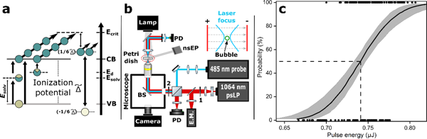
Optical and electrical breakdown of materials, which describe material modification in the presence of extreme optical or electrical fields, have been studied since the 1950s. However, simultaneous application of optical and electrical fields, especially, to biologically relevant systems hasn't been explored before. Prof. Vladislav V. Yakovlev from Texas A&M University said by investigating the synergistic action of electrical and optical pulses, they were able to promote highly localized breakdown, while reducing the threshold for such breakdown.
Photonics Research
- Apr. 07, 2021
- Vol. 9, Issue 3 (2021)
Editors' Picks
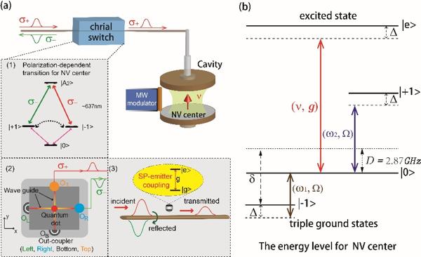
In the quantum optics research area, a central goal is to develop techniques for a complete control of light-matter interaction at the single-quantum level, which underlies the essential physics of many phenomena and applications. A new quantum revolution on optics and photonics is also accelerating the progress of quantum information processing (QIP), with the rapid innovation of the advanced photonic nanomaterials and processing technologies.
Photonics Research
- Mar. 26, 2021
- Vol. 9, Issue 3 (2021)
Editors' Picks
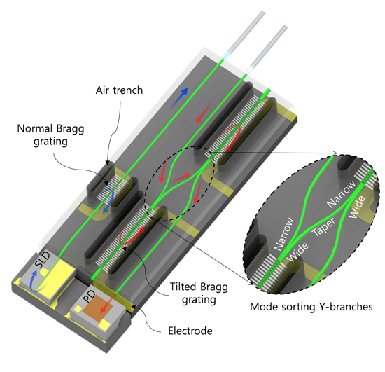
Recent explosive expansion of web-based video platform services pushes the data traffic increase enormously, and has become a driving force in the development of the next-generation communication technologies. The number of communication channels in optical communication is upgraded by using the wavelength division multiplexing (WDM) technology. The bottleneck of communication capacity occurs at the fronthaul connecting radio-access networks of 5G communication.
Photonics Research
- Mar. 17, 2021
- Vol. 9, Issue 2 (2021)
Editors' Picks
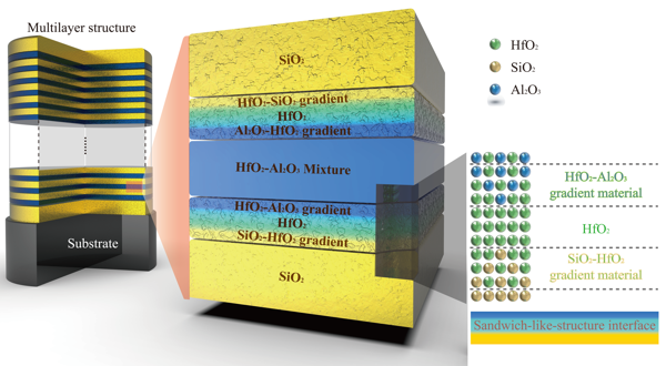
Dichroic laser mirrors are usually used as harmonic separators, beam combiners or splitters, and play an important role in many laser applications, including inertial confinement fusion laser, petawatt femtosecond laser, high power fiber lasers, compact Q-switched or mode-locked lasers, and other emerging lasers.
Photonics Research
- Mar. 11, 2021
- Vol. 9, Issue 2 (2021)
Editors' Picks
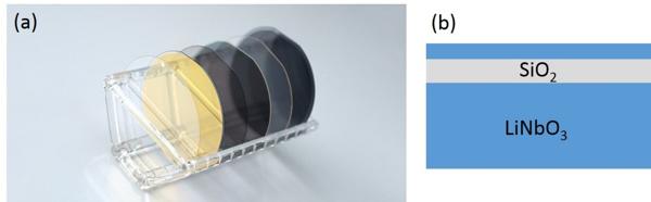
Over the past decades, the advent and development of electronic integrated circuits and optical communication technology has brought the global human society into the "Information Explosion" era. Recently, owing to the soaring demand on information exchanging and processing speed and efficiency, photonic integrated circuit (PIC) has attracted tremendous interest for the potential to provide the better performances than its electronic counterpart.
Photonics Research
- Mar. 09, 2021
- Vol. 8, Issue 12 (2020)
Editors' Picks
The interference phenomenon forms the most important evidence of the wave-like property of light. The phase of the wave is the key concept underlying the interpretation of constructive and destructive interferences of superposed light beams. On the other hand, it is known that even when light is considered as a particle or photon, a single photon can interfere with itself. Although light exhibits both wave- and particle-like properties, the linear superposition of the field amplitudes for light waves is the same as that of the probability amplitudes of a photon in the case of first-order interference.
Photonics Research
- Feb. 23, 2021
- Vol. 9, Issue 1 (2021)
Editors' Picks
Optical modulators provide the information encoding engines for most long-haul terrestrial and undersea fiber-optic transmission systems. The Internet that connects the people and businesses around the world can be possible because of the widespread of reliable, low-loss and high-speed optical modulators. As the trend toward ever-increasing bandwidths in fiber-optic communications continues, the optical modulator will remain an indispensable component for transmitting information. Today, hundreds of millions of modulators have been deployed worldwide, and many of them are lithium niobate (LiNbO3) modulators.
Photonics Research
- Jan. 08, 2021
- Vol. 8, Issue 12 (2020)
Editors' Picks
With the booming development of cloud services, artificial intelligence (AI) and 5G applications, the explosive growth of global traffic requires higher and higher bandwidth of data center interface. As the 400GbE standard has been approved as IEEE Std 802.3bs, more and more researches are focusing on next generation of 800 Gb transceiver technology and its standard.
Photonics Research
- Dec. 18, 2020
- Vol. 8, Issue 11 (2020)
Editors' Picks
InGaN-based materials have broad application prospects in visible light range due to its tunable wide band-gap. Micro size light emitting diode (micro-LED) display is one of the most promising applications. Future smart phones, watches, virtual reality glasses, and other small screens will benefit from micro-LED technology.
Photonics Research
- Nov. 26, 2020
- Vol. 8, Issue 11 (2020)
Editors' Picks
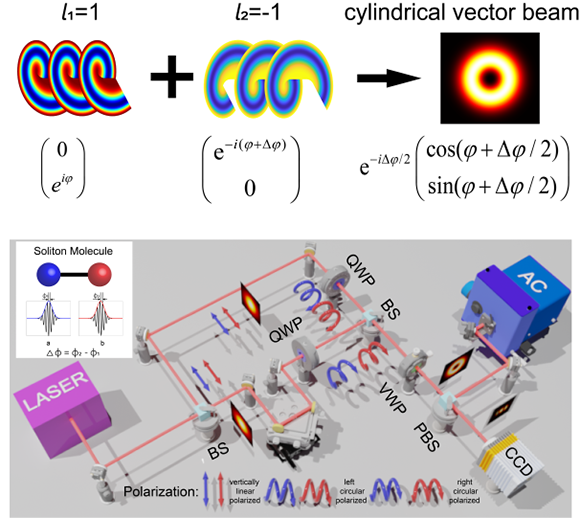
Solitons, non-spreading wave structures, are universal in a variety of research fields that ranging from fluid and condensed matter physics to chemistry and neurobiology. Optical solitons can be formed and propagated in laser cavities with remarkable stability thanks to a double balance between loss and gain and between dispersion and nonlinearity. Optical solitons show particle-like interactions and can form various bound states akin to chemical molecules, which are frequently referred as soliton molecules. Soliton molecules have attracted tremendous attention due to their potential to upgrade the transmission capability of optical communication and to demonstrate complex soliton interaction behaviors in dynamical nonlinear systems.
Photonics Research
- Oct. 29, 2020
- Vol. 8, Issue 10 (2020)
Editors' Picks
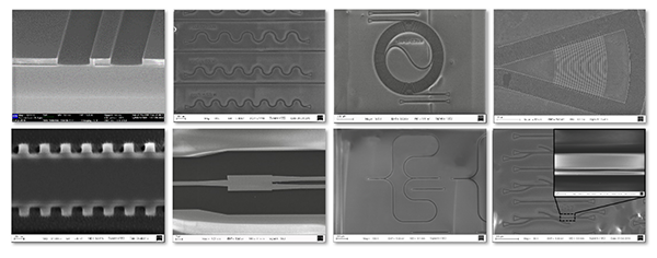
In recent years, the 2 μm waveband has attracted increasing research for broad applications, including optical communication, optical sensing, and even the next generation of gravitational-wave observatories. Particularly, thanks to hollow-core fibers with low latency and low loss in an ultrawide bandwidth, and thulium (Tm) doped fiber amplifiers with a broad gain spectrum, 2 μm possesses the promising application of next-generation optical communication with ultralow latency and further higher capacity. Several 2 μm optical short-reach interconnections over hollow-core fibers have been carried out in our previous works, achieving a record single-lane speed of 100 Gbps. Meanwhile, the photonic integrated platform for 2 μm optical interconnection is also an essential field that needs to be exploited.
Photonics Research
- Oct. 09, 2020
- Vol. 8, Issue 9 (2020)
Editors' Picks
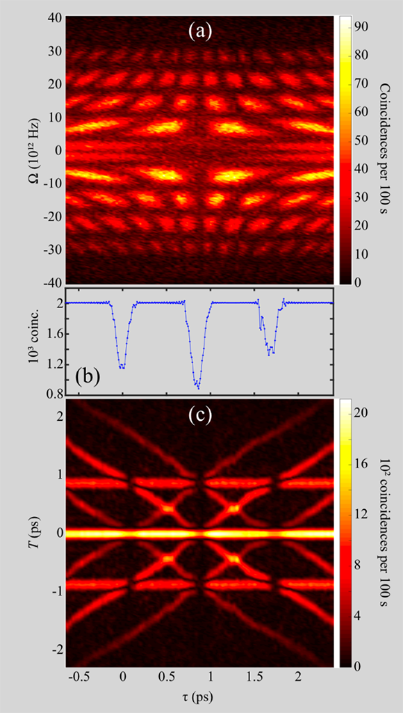
Quantum optical coherence tomography (QOCT) was proposed some time ago as a highly promising alternative to its classical counterpart for obtaining morphological information of semi-transparent, e.g. biological, samples. In particular, since the time when QOCT was first proposed two key advantages were identified with respect to an equivalent classical system: even-order dispersion cancellation in the sample under study, as well as a factor-of-two improvement in axial resolution. However, the low-flux nature of photon pair sources and the resulting long times of data acquisition, have severely limited the practical applicability of QOCT. Our present work aims to overcome some of these limitations through the implementation of a Fourier domain version of the technique which eliminates the need for axial scanning.
Photonics Research
- Sep. 10, 2020
- Vol. 8, Issue 6 (2020)
Editors' Picks
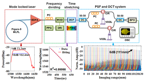
High-performance swept sources with high sweep rate, flat spectrum, wide sweep range and long coherence length will find applications in many photonic systems, especially in optical coherence tomography (OCT) and LiDAR. OCT technology was rapidly commercialized after its invention by D. Huang et al. in 1991. Swept source OCT is a promising candidate to satisfy the increasing demand for real-time high-speed imaging in the next generation OCT. In a swept source OCT system, a single-point high-speed photodetector is utilized to acquire the interference signal of the reflected light from the reference arm and the sample arm of the Michelson interferometer. The axial scan rate can be up to tens of millions of scans per second benefiting from the high-speed photodetector and the motionless configuration. When the bandwidth of the photodetector is sufficiently large, the performance of the swept source OCT depends predominantly on the performance of the swept source. MEMS-VCSEL, Fourier domain mode locked laser, and time-stretched swept laser have been proposed to be the swept sources of megahertz OCT. Among them, the swept source based on time-stretching is the only technology that has demonstrated sweep rates higher than 10 MHz. A highly coherent seed laser with a high repetition rate and a broad flat spectrum is the key to generate high performance time-stretched swept source. The spectrum of mode locked fiber laser output however is not sufficiently broad for time stretching. Supercontinuum can achieve a broad spectrum but suffers from the large shot-to-shot spectral fluctuation, which impedes its application in time-stretching. Finally, reconfiguration of time-stretched swept sources to operate at different sweep rates has not been demonstrated.
Photonics Research
- Sep. 10, 2020
- Vol. 8, Issue 8 (2020)
Editors' Picks
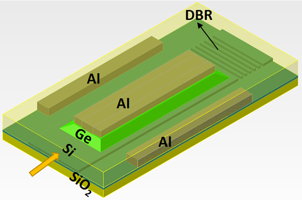
Data communications in data centers and high-performance computing (HPC) have grown tremendously due to emerging applications in social media, video streaming, artificial intelligence (AI), and the internet of things (IoT). Hyperscale data centers and Exascale HPC require high-bandwidth and energy-efficient optical interconnects. In this context, silicon photonic interconnects are attractive, thanks to the high integration and low cost. To further increase the data rate, advanced modulation formats are preferred which can relax the bandwidth limitation of integrated circuitry or optical devices. However, the optical link may suffer degraded signal-to-noise ratio (SNR), which requires either a higher-power laser or a higher-sensitivity receiver to retain the bit error rate (BER). Using a receiver with better sensitivity can yield a lower total link power consumption compared to using a high-power laser and consequently improve the energy efficiency. Particularly, high-sensitivity detectors relax the link budget requirements for on-chip lasers with limited output power. An avalanche photodiode (APD) with internal gain is the ideal candidate to increase the receiver sensitivity. Since APDs introduce the excess noise while bringing the multiplication gain, a novel device structure with optimum layer thickness and doping profile is necessary for higher gain and lower noise. Typically, there are trade-offs among APD design metrics: breakdown voltage, quantum efficiency, multiplication gain, bandwidth, and excess noise. It is a big challenge to decouple these trade-offs and optimize the overall performance.
Photonics Research
- Sep. 03, 2020
- Vol. 8, Issue 7 (2020)
Editors' Picks
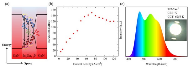
Visible light communication (VLC) is a wireless method that enables high-speed transmission of data with visible light. This data is transmitted by modulating the intensity of light given off by a light source. The signal is received by a photodiode device that transforms the data into forms that are readable and readily-consumed by end users. It is widely expected that VLC systems and their extension to fully networked, bi-directional multiuser wireless systems referred to as LiFi will play a key part in 5G-and-beyond connectivity, especially for indoor environments.
Photonics Research
- Sep. 03, 2020
- Vol. 8, Issue 7 (2020)
Editors' Picks
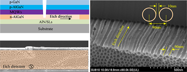
UVC-LEDs with light emission from 200-280 nm were mainly used to introduce germicidal radiation to microorganisms (bacteria, viruses, spores and other pathogens). It damages and changes the structure of DNA (deoxyribonucleic acid), so that the microorganisms die or loss the reproduction capability immediately, and achieve the purpose of sterilization and disinfection. UVC-LED has a great market potential with a wide range of applications in air sterilization, surface disinfection and water treatment, because of its stability and safety, environmental friendliness, long lifetime, low maintenance cost and zero chemical residue. However, the biggest challenge for the UVC-LED is its low external quantum efficiency and insufficient output optical power density under high current. In addition to the poor quality of the Al-rich UVC epitaxial material and the low injection efficiency of the carrier, the main reason for the low quantum efficiency is due to the low extraction efficiency of TM mode (E//C) photons. TM mode UVC photons are confined in the epitaxial layer and suffer from the total internal reflection and re-absorption. Previous methods known to improve the light extraction of visible LEDs have little effect on TM mode light in the UVC-LED.
Photonics Research
- Jul. 30, 2020
- Vol. 8, Issue 6 (2020)
Editors' Picks
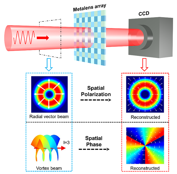
The amplitude, phase, and state of polarization (SOP) are fundamental parameters for describing light waves. The real-time measurement of the polarization and phase information of light is very important and desirable in optics. At present, however, most photodetectors are only sensitive to the light intensity, which makes traditional polarization and phase detection systems complex, bulky and difficult to integrate.
Photonics Research
- May. 21, 2020
- Vol. 8, Issue 4 (2020)
Editors' Picks
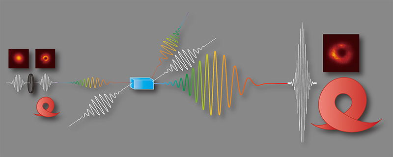
An optical vortex refers to a beam whose wavefront shows a helical shape. Compared with the conventional Gaussian beam, since the optical vortex has doughnut intensity distribution and orbital angular momentum (OAM), it has acquired considerable interest in quantum information, optical trapping and manipulation, super-resolution microscopy and high-order harmonic generation (HHG). Spurred by these exciting technologies, widespread attention has been paid to the generation and manipulation of optical vortex. However, due to the low damage threshold and transmittance of optical components, it is difficult to directly generate high-energy mid-infrared (mid-IR) femtosecond optical vortex pulses using spiral phase plates (SPPs), spatial light modulators (SLMs), etc. Optical parametric chirped pulse amplification (OPCPA), combining optical parametric amplification (OPA) and chirped pulse amplification (CPA) technologies, displays unique advantages, such as high gain, high temporal contrast, less thermal effect and tunable wavelength, and it has been widely employed in recent high peak power laser systems. Therefore, OPCPA is able to be an effective technology to generate high energy femtosecond mid-IR optical vortices.
Photonics Research
- Apr. 30, 2020
- Vol. 8, Issue 3 (2020)
Editors' Picks
Due to its excellent electro-optical and nonlinear optical properties, paired with a relative easiness of fabricating waveguides, the lithium niobate (LN) crystal has its place as an ideal platform for highly efficient and compact devices for quantum and/or classical optical applications. Up to now, most of commercially available integrated optics devices are based on LN waveguides fabricated either by Ti-indiffusion or by one of the conventional liquid-phase Proton Exchange techniques. These techniques allow fabricating waveguides with preserved electro-optical and nonlinear properties but, unfortunately, exhibiting low-index contrast typically in the range of 0.01 and 0.03. These low values limit the benefit linked to the confinement of the light in a waveguide. In this context, the challenge of modern photonics based on LN is to provide integrated configurations that ideally meet all these requirements: high-index contrast, low propagation losses, undegraded optical nonlinearity and electro-optical efficiency, stability, robustness, compactness, easiness of implementation, and low power consumption.
Photonics Research
- Apr. 01, 2020
- Vol. 8, Issue 1 (2020)
Videos

The second interview for a Photonics Research (PR) webinar series took place on 28 November 2022. Assistant Editor of PR, Prof. Lin Chang from Peking University interviewed Prof. John Bowers, University of California-Santa Barbara, United States. Nevertheless, Prof. Bowers was the doctoral supervisor of Lin Chang. Prof. Bowers is one of the founders of Silicon-based Photonics. He is a member of the National Academy of Engineering, the National Academy of inventors, a fellow of the IEEE, OSA and the American Physical Society. He is a recipient of the EEE Photonics Award, OSA/IEEE Tyndall Award, the OSA Holonyak Award, the IEEE LEOS William Streifer Award and the South Coast Business and Technology Pioneer and Entrepreneur of the Year Awards. He is a cofounder of Aurrion, Aerius Photonics and Calient Networks. He has published two books, ten book chapters, 450 journal papers, 1000 conference papers and has received 54 patents. He and coworkers received the EE Times Annual Creativity in Electronics (ACE) Award for Most Promising Technology for the hybrid silicon laser in 2007. The full transcript is provided below.
Photonics Research
- Nov. 10, 2023
- Vol. , Issue (2023)
Videos
Recording of presentations from Photonics Research Workshop: Integrated Photonics, 7 Aug 2022, Xi'an, China
Photonics Research
- Oct. 11, 2022
- Vol. , Issue (2022)
Videos
Yu-Sheng Lin, Sun Yat-Sen University, China;
Lai Wang, Tsinghua University, China
Photonics Research
- Sep. 13, 2022
- Vol. , Issue (2022)
Videos
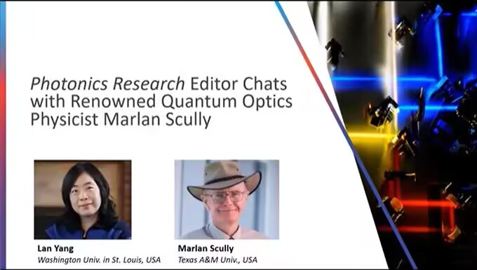
The first interview for a Photonics Research webinar series took place on 26 May 2021. Editor in Chief, Prof. Lan Yang interviewed Prof. Marlan Scully, Texas A&M University, United States. He is a world leader in the field of quantum optics and has made numerous groundbreaking discoveries that include the first quantum theory of lasers with Willis Lamb, the first demonstration of lasing without inversion, and the first demonstration of ultra-slow light in in hot gases, just to name a few.
Photonics Research
- Dec. 10, 2021
- Vol. 10, Issue 1 (2022)
News

Integrated photonics enables the synthesis, processing and detection of optical signals using photonic integrated circuits (PICs). It has rapidly transformed numerous fields and applications by enabling faster and more efficient ways to process and transmit information, as well as new techniques for telecommunications, sensing, medical diagnosis, and quantum computing, just to name a few. With its intrinsic high speed, large bandwidth, and unlimited parallelism, integrated photonics plays a critical role in handling high-throughput, data-intensive applications. Over the past few decades, the successful translation from laboratory research to commercial deployment has established integrated photonics as a standard technology widely used in high-data-rate telecommunications and datacenters. With the development of heterogeneous integration for various material platforms, researchers have demonstrated myriad novel devices, including miniaturized classical and quantum light sources, micro-resonator frequency combs, ultrafast electro-optic modulators, programmable MEMS-controlled circuits, and large-scale on-chip photonic networks. These advancements are continuously impacting our society and opening up new opportunities in areas such as optical communications, photonic computing, frequency metrology, and LiDAR.
Photonics Research
- May. 19, 2023
- Vol. , Issue (2023)
News
Optical microresonators have been one of the most active and exciting research topics in the photonics community in recent years. By confining light in both spatial and time domain, optical microresonators serve as an indispensable platform for significantly enhancing light–matter interaction and controlling light fields at the micro- and nano-scale. These capabilities make optical microresonators important tools for a wide range of applications, including sensing, metrology, communication, and quantum computing.
Photonics Research
- May. 19, 2023
- Vol. , Issue (2023)
News

Career Insights from Professor John Bowers
Photonics Research
- Nov. 16, 2022
- Vol. , Issue (2022)
News
"A new blue light emitting diode with high modulation bandwidth for high-speed visible light applications was demonstrated by a research team including researchers from three institutes. The technological development in this work represents a typical multidisciplinary study with scientific discoveries from multiple fields, including materials synthesis, device fabrication, system integration and characterization. Such a study is a great example showing the power of teamwork accomplished by researchers covering different aspects of scientific fields to achieve something with societal impacts beyond what can be achieved by a single group." Editor-in-Chief Prof. Lan Yang comments.
Photonics Research
- Sep. 05, 2022
- Vol. 9, Issue 5 (2022)
News
"The design of tunable metamaterials is extremely important for many applications. Integration of micro-electro-mechanical system (MEMS) with metamaterials is very promising direction to achieve reconfigurable capabilities. In this paper, the authors propose and demonstrate with high-quality sophisticated fabrication a reconfigurable and programmable MEMS-based metadevice with multifunctional characteristics to simultaneously perform the logic operations. This study makes an important contribution to the future developments of smart and tunable metadevices." Deputy Editor Prof. Yuri Kivshar comments.
Photonics Research
- Jul. 28, 2022
- Vol. , Issue (2022)
News

Recently, Optica (formerly OSA) announced that Yuri Kivshar, Australian National University, Deputy Editor of Photonics Research, has been selected as the 2022 recipient of the Max Born Award. Kivshar is honored for pioneering and ground-breaking research in nonlinear metamaterials and all-dielectric resonant metaphotonics that derives unique optical functionalities from electric and magnetic dipolar and multipolar Mie-type resonances underpinning new discoveries in nonlinear and topological nanophotonics.
Photonics Research
- Mar. 24, 2022
- Vol. , Issue (2022)
News

At the opening ceremony of the 12th International Conference on Information Optics and Photonics on July 24th (CIOP 2021, Xi'an, China), Prof. Zhiyi Wei from Institute of Physics, Chinese Academy of Sciences, the Technical Program Chair, announced the 2020 Editor-in-Chief Choice Awards of Photonics Research and Chinese Optics Letters.
Photonics Research
- Aug. 04, 2021
- Vol. , Issue (2021)
News
Silicon photonics has been developing at an increasingly fast pace with many passive and active silicon photonic devices demonstrated with unprecedented performances. Large-scale silicon photonic circuits have been realized with high integration density for many applications ranging from telecom and Datacom to sensing, metrology, and quantum photonics. This special issue aims to provide a comprehensively overview of this exciting field, including recent progress, in-depth discussions of the state-of-the-art, and insights into forthcoming developments from world's most prominent research groups driving silicon photonics technology into its next-generation phase.
Photonics Research
- May. 25, 2021
- Vol. , Issue (2021)
News
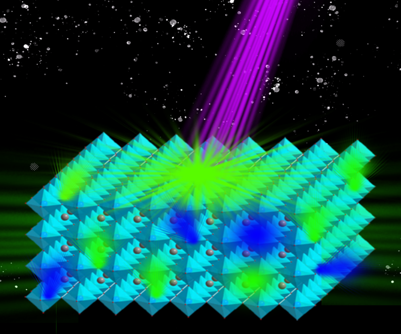
Recent progress in photonics research has led to the discovery of novel optical materials, in which metallic halide perovskites plays a large role for semiconductor photonics. Owing to their stunning optical properties, perovskites have been widely considered as promising platforms for the manipulation of photons in free space/matter based on bulk and low-dimensional systems. Recently, a series of significant efforts and breakthroughs in perovskite photonics have been reported by institutions and companies around the world, opening a bright path to demonstrating next-generation excellent-performance, low-consumption optoelectronic devices.
Photonics Research
- Feb. 24, 2020
- Vol. 8, Issue (2020)
News
This feature issue in Photonics Research will serve as a venue for the most recent publications in the areas of emerging topological photonics and beyond, reporting recent results and innovative approaches for integrating topological physics in photonics with nonlinear, synthetic, or quantum photonic systems.
Photonics Research
- Feb. 24, 2020
- Vol. 8, Issue (2020)
Special Issue
Guest Editors
Liang Feng, University of Pennsylvania, USA (Lead Editor)
Junqiu Liu, Shenzhen International Quantum Academy, China
Cheng Wang, City University of Hong Kong, China
Photonics Research
- May. 19, 2023
- Vol. , Issue (2023-2024)
Special Issue
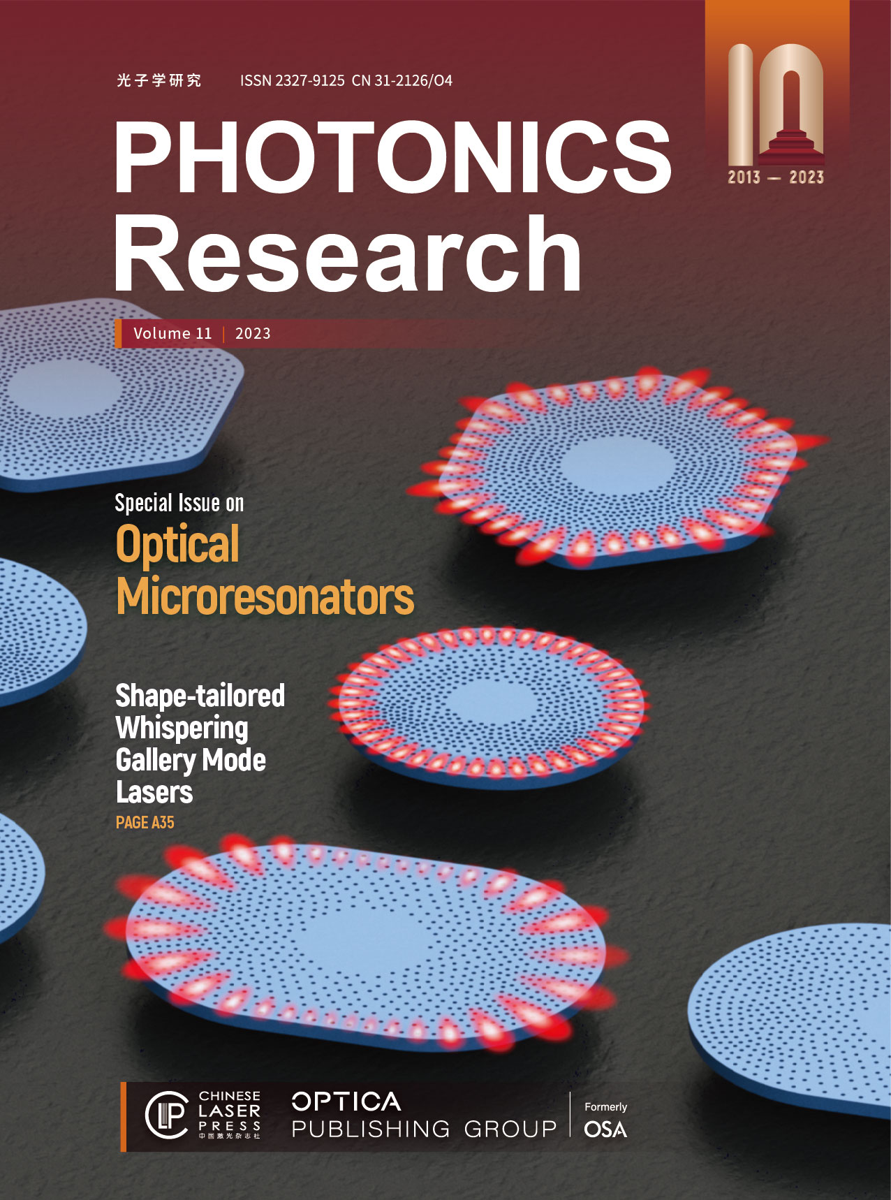
Guest Editors
Yun-Feng Xiao
Peking University, China (Lead Editor)
Kartik Srinivasan
National Institute of Standards and Technology (NIST), USA
Pascal Del’Haye
Max Planck Institute for the Science of Light, Germany
Mengjie Yu
University of Southern California, USA
On the Cover of the virtual issue
Deformed shape microcavity lasers based on transformation optics are demonstrated for the first time, which exploit whispering gallery modes (WGMs) free from Q-degradation. Q spoiling caused by the boundary shape deformation is recovered by spatially varying nanohole density distribution.
Photonics Research
- May. 19, 2023
- Vol. , Issue (2023)
Special Issue

Guest Editors:
Guixin Li
Southern University of Science and Technology, China (Lead Editor)
Thomas Pertsch
Friedrich-Schiller-Universität Jena, Germany
Arka Majumdar
University of Washington, USA
Shumin Xiao
Harbin Institute of Technology (Shenzhen), China
On the Cover of the virtual issue
Oscillatory spin splitting along the optical path enabled by two-channel Pancharatnam-Berry phase metalens.
Photonics Research
- Oct. 28, 2022
- Vol. , Issue (2022-2023)
Special Issue
Guest Editors:
Daoxin Dai,
Zhejiang University, China (Lead Editor)
Di Liang,
Hewlett Packard Enterprise, USA
Pavel Cheben,
National Research Council of Canada, Canada
On the Cover of the virtual issue
Heterogeneous integration enables high-performance active and passive silicon nitride photonic integrated circuits. Narrow-linewidth lasers and laser soliton microcombs based on silicon nitride are projected to be critical in applications including optical interconnects, sensing, microwave photonics, metrology, and so on. See Chao Xiang et al., page A82.
Photonics Research
- May. 25, 2021
- Vol. 9, Issue (2022)
Special Issue
Guest Editors:
Zongfu Yu,
University of Wisconsin, Madison, USA (Lead Editor)
Yang Chai,
The Hong Kong Polytechnic University, China
Li Gao,
Nanjing University of Posts and Telecommunications, China
Darko Zibar,
Technical University of Denmark, Denmark
On the Cover for this virtual special issue
A new deep compressed imaging modality enables high speed image acquisition and high fidelity object reconstruction. See Kangning Zhang et al., page 03000B57.
Photonics Research
- Jun. 30, 2021
- Vol. 9, Issue (2021)
Special Issue
Guest Editors:
Andrea Alu,
City University of New York, USA (Lead Editor)
Jingyun Fan,
Southern University of Science and Technology, China
Laura Pilozzi,
National Research Council, Italy
Haitan Xu,
Peking University, China
On the Cover for this virtual special issue
Topological photonics opens a new avenue to understand varieties of exotic and novel photonic phenomena, and it is expected to boost a series of key applications of photonics and optoelectronic in many aspects. See Xuefan Yin et al., page 11000B25.
Photonics Research
- Feb. 24, 2020
- Vol. 8, Issue (2020)
Special Issue
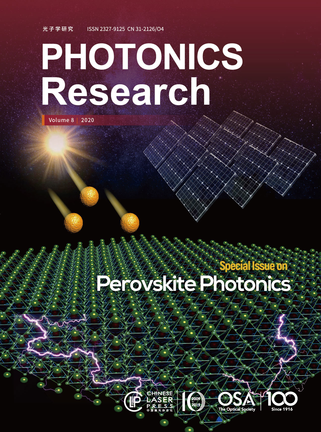
Guest Editors:
Qing Zhang,
Peking University, China (Lead editor)
Carole Diederichs,
Sorbonne University, France
Qihua Xiong,
Nanyang Technological University, Singapore
On the Cover for this virtual special issue
Large area perovskite solar cells: the way for application. See Yang Zhao et al., page 070000A1.
Photonics Research
- Feb. 24, 2020
- Vol. 8, Issue (2020)
Special Issue
Quantum photonics is an increasingly important emerging field because of the rising demand for experimental demonstration of quantum communication, quantum computing, and quantum simulation, and photonic chips possess prominent advantages as a potential analog for digital quantum computers and a versatile tool for probing fundamental quantum physics.
Using the photonic structure to form a large state-space not only may be fundamentally interesting but also may provide a powerful platform for quantum simulation and quantum computing. This Feature Issue will explore the use of photonic platforms to investigate quantum advantage/supremacy in various quantum computing protocols, such as Boson sampling, quantum walk, fast hitting, and even universal quantum computing protocols.
Photonics Research
- Mar. 13, 2019
- Vol. 7, Issue (2019)
Special Issue
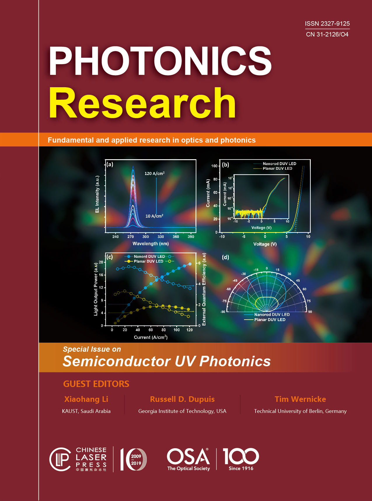
UV light has been utilized by people in numerous critical applications for over 100 years. However, mainstream UV emitters and detectors are often bulky and inefficient. Recently, large investment and progress have been made by institutions and companies around the world to create and improve semiconductor materials, structures, and devices for more efficient generation and manipulation of UV light with a much smaller footprint and better reliability. This feature issue will cover modeling, experimentation, and applications related to UV photonics research and its applications.
This feature issue in Photonics Research will serve as a venue for the most recent publications in the increasingly popular research area of semiconductor ultraviolet (UV) photonics, which has found broad applications in sterilization, communication, sensing, curing, medical treatment, and national security.
Photonics Research
- Mar. 13, 2019
- Vol. 7, Issue (2019)
Special Issue
The emergence of graphene saturable absorbers towards the generation of ultra-short pulses in mode-locked lasers have significantly attracted world-wide attention in the related fields. Graphene-based saturable absorbers have been verified to possess unique properties, such as broad operation bandwidth, ultrafast response time, relatively high modulation depth and low saturation intensity. Inspired by the great success of graphene, graphene-like two-dimensional (2D) layered materials have also been demonstrated for ultrafast pulse generation with distinctive advantages of tunable bandgap, low optical losses, high optical nonlinearities. This feature issue is aimed at scientists, engineers and practitioners interested in understanding the novel nonlinear optical properties of 2D materials and exploring their potential applications in mode locked lasers.
Photonics Research
- Mar. 13, 2019
- Vol. 6, Issue 10 (2018)
Special Issue
The idea of parity-time (PT) symmetry, first introduced in quantum mechanics, was recently realized in the context of photonics in the form of balanced gain-loss structures with special symmetries. In recent years, these systems have been shown to have many exotic features and behaviors with various potential applications, including unidirectional invisibility, coherent perfect absorption, negative refraction, novel laser designs, optical isolation, and unusual wave diffraction dynamics. One of the main characteristics of such non-Hermitian configurations is the existence of abrupt effective phase transitions that occur when the gain-loss amplitude exceeds a certain threshold value, providing even greater control over device design and functionality. More general gain-loss structures can exhibit an even richer variety of non-Hermitian optical properties, and the breadth of these properties has yet to be fully explored. This special issue is on a wide range of recent developments in the new area of parity-time (PT) symmetric and Non-Hermitian Optics, considering theoretical, experimental, and practical aspects of synthetic structures that contain gain and loss.
Photonics Research
- Mar. 13, 2019
- Vol. 6, Issue 8 (2018)
Special Issue
Advances in integrated optoelectronics and nanophotonics have been very rich in recent years. These include the spectacular developments of nonlinear group four photonic platforms as well as the integration of components and functions based on III-V semiconductor materials. One of the strongest trends for the future is the development of all-optical signal processing functions within integrated, compact, low-loss devices, paving the way for new applications. This approach, relying on materials, components and the integration of optical functions, is based on a wide range of exciting physical phenomena, exploiting the nonlinear optical response of materials for the generation of frequency combs, the conversion of light wavelength, the generation of supercontinuum radiation, and many other phenomena exploiting the unprecedented power of light control by waves. This special issue has drawn a critical overview of the recent and significant burgeoning advances in the field, as well as to identify the next technological and scientific milestones to come for the development of integrated nonlinear photonics. Meanwhile, it aims to shed light on the interdisciplinary dimension of the work carried out in the field, based, for example, on the control of optical waves by acoustic waves, opening the way to the fields of nonlinear optomechanics and optoacoustics.
Photonics Research
- Mar. 13, 2019
- Vol. 6, Issue 5 (2018)
Special Issue

Optical microcavities have attracted tremendous interests in both fundamental and applied research in the past few decades, thanks to their small footprint, easy integrability, and high quality factors. Using total internal reflection from a dielectric interface or photonic band gaps in a periodic structure, these devices do not rely on conventional metal-coated mirrors to confine light in small volumes, which have brought forth new developments in both classical and quantum optics.
Photonics Research
- Mar. 13, 2019
- Vol. 5, Issue 6 (2017-2018)
Special Issue

Light-emitting diode (LED) technology has advanced considerably over the last few decades, yet many device physics mechanisms remain not well understood, and performances at certain wavelengths (especially deep ultraviolet, as well as the green wavelength regime) leave much room for improvement. This special issue of original research articles focus on all aspects of light-emitting diode (LED) technology.
Photonics Research
- Mar. 13, 2019
- Vol. 5, Issue 2 (2017)
Special Issue

This special issue focuses on optical vortices and solicits original papers on all aspects of optical vortices.
Photonics Research
- Mar. 13, 2019
- Vol. 4, Issue 5 (2016)
Special Issue

This special issue discusses advancements in terahertz technology relating to both instrumentation and material characterization. Terahertz systems have come a long way since the first demonstration of terahertz generation using photonics. New methods to utilize and manipulate terahertz light are evolving which in turn facilitate improved material characterization and opportunities for new applications.
Photonics Research
- Mar. 13, 2019
- Vol. 4, Issue 3 (2016)
Special Issue

Integrated Photonics, which has achieved great success since Integrated Photonics was proposed by Dr. Miller in 1969. Currently various materials and technologies have been developed to realize photonic integrated circuits for many applications. The comprehensive reviews for the state-of-the-art for all aspects of integrated photonics will be very helpful for this field. It is even more important to have a deep discussion on the challenges and perspectives for integrated photonics, which will be definitely very beneficial for the young scientists and students.
Photonics Research
- Mar. 13, 2019
- Vol. 3, Issue 5 (2015)
Special Issue

Photonics Based on Two Dimensional Materials
Photonics Research
- Mar. 13, 2019
- Vol. 3, Issue 2 (2015)
Special Issue

This special issue on Microwave Photonics provides participants of the Asia Communications and Photonics Conference (ACP) 2013 with the opportunity to publish an account of their microwave photonics research as a peer-reviewed archival paper in the Journal. While meeting participants are particularly encouraged to submit their work, the special issue is open to all contributions in this particular area.
Photonics Research
- Mar. 13, 2019
- Vol. 2, Issue 4 (2014)
Special Issue

The scope of this special issue on Group Four Photonics spans all aspects (both basic science and device applications) of photonics related research involving the use of group IV elements (carbon, silicon, germanium, tin, etc.). Example topics include novel passive silicon photonics, nonlinear silicon photonics, active silicon photonics, hybrid III-V on silicon lasers, germanium-based photodetectors, lasers or modulators, graphene photonics, diamond photonics and photonics using organic materials.
Photonics Research
- Mar. 13, 2019
- Vol. 2, Issue 3 (2014)
PR Highlights
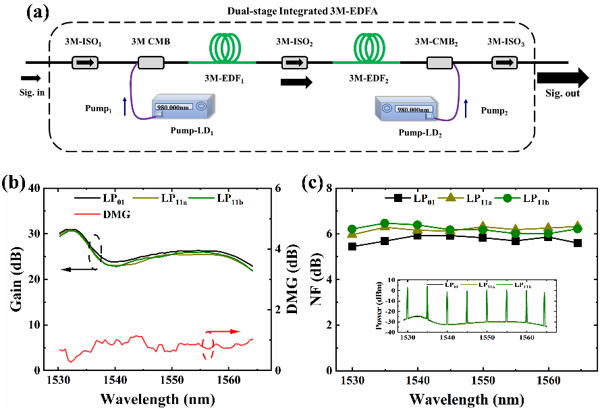
There is burst growth in the demand for network capacity, with the rapid development of new technologies, such as big data and cloud computing, etc. As the cornerstone of the global network, the traditional communication system based on the single-mode fiber has been rapidly developed for nearly 50 years. Its capacity has approached the nonlinear Shannon limit, which cannot meet the demand of network bandwidth surge. Mode-division multiplexing (MDM) technology based on multiple orthogonal modes in few-mode fibers (FMFs) is expected to overcome this capacity crunch.
Photonics Research
- Feb. 09, 2023
- Vol. 10, Issue 12 (2023)
PR Highlights
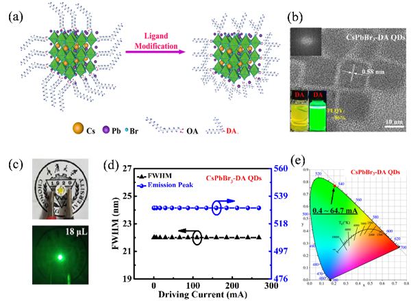
Currently, commercial displays and lighting sources are commonly fabricated using red, green and blue LEDs. In general, those three different LEDs correspond to different luminescent materials with different lifetimes. With the efficiency of red, green and blue LEDs varies greatly, light-emitting devices suffer problems of color shift after being used for a period, affecting the display performance.
Photonics Research
- Aug. 04, 2021
- Vol. 8, Issue 7 (2021)
PR Highlights
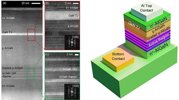
Every year, thousands of lives and billions of dollars are spent worldwide as a result of health-care associated and waterborne illnesses. Sterilization is a critical preventative measure and it can be achieved by a number of techniques including irradiation using ultraviolet (UV) light.
Photonics Research
- Aug. 04, 2021
- Vol. 8, Issue 3 (2021)
PR Highlights
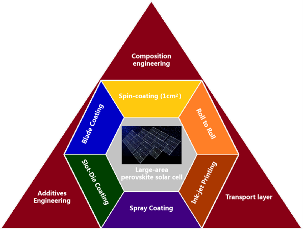
The record power conversion efficiency of perovskite solar cells (PSCs) has impressively exceeded 25% in 10 years due to composition engineering, perovskite film growth control and perovskite/transport layer interface modification. However, the high efficiency PSCs are usually small-area (<0.1 cm2). For commercial application, the preparation of large-area devices is the necessary step for the development of PSCs.
Photonics Research
- Jan. 05, 2021
- Vol. 8, Issue 7 (2020)
PR Highlights
As a candidate for the next generation display technology, micro-LED has the potential to replace LCD and OLED display technology. However, micro-LED still faces some difficulties that need to be overcome. First is the wavelength stability of micro-LED chips. The micro-LED device needs to dynamically adjust the operation current according to the intensity of ambient light, so the wavelength of the Micro-LED will shift significantly, resulting in serious color shift. Second is the fabrication of the quantum-dot color-conversion layer. the traditional spray process is still too slow to fabricate commercial quantum-dot color-conversion layers.
Photonics Research
- Jun. 12, 2020
- Vol. 8, Issue 5 (2020)
PR Highlights
3D and flexible devices benefit from many advantages over their rigid counterparts, including amenability to large-area, low-cost fabrication via roll-to-roll processing, and the possibility of conformal integration on curvilinear surfaces or biological tissues. Following in the footsteps of the widely successful 3D electronics, 3D integrated photonics has recently attracted increasing attention in an effort to provide the same deployment flexibility to optical systems, with applications covering biotechnology, sensing, 3D manufacturing, optical interconnects, and others. 3D integrated photonics is thus poised to expand the reach of photonics by enabling both the extension of traditional applications to non-planar geometries and adding novel functionalities that cannot be attained with planar devices.
Photonics Research
- Apr. 16, 2020
- Vol. 8, Issue 2 (2020)
PR Highlights
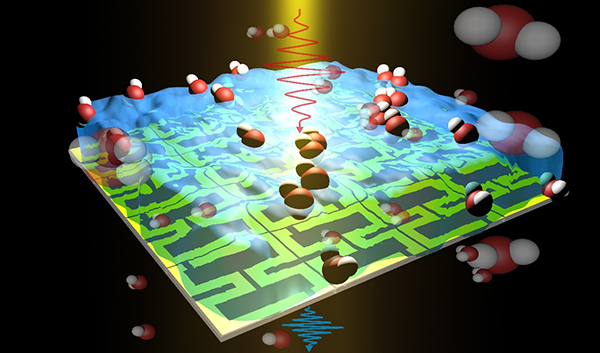
Metamaterials, composed of periodic arrangements of artificial sub-wavelength unit cells, have aroused great attention in the scientific community due to their novel optical properties. The well-known basic block is plasmonic split-ring resonators (SRRs). Based on the design of the geometric configuration, they exhibit excellent modulation performance for terahertz waves (THz). However, the fixed structures of SRRs make it difficult to actively modulate THz waves owing to unalterable resonant characteristics. Although the methods of applying external electric and optical fields to change the electromagnetic characteristics of SRRs, and thus achieving active modulation have been reported, the complicated heterostructure fabrication and optical measuring systems have also bring certain difficulties in experiments.
Photonics Research
- Mar. 30, 2020
- Vol. 7, Issue 12 (2019)
PR Highlights
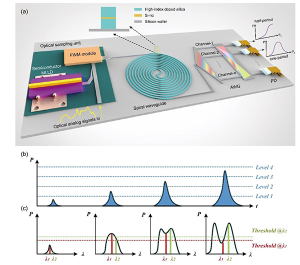
Analog-to-digital converters (ADCs) along with their counterparts the digital-to-analog converters (DACs) are an indispensable link between our analog physical world and the virtual digital world where data are stored and processed digitally. Besides, the transmission of such data is required to be at high-speed in the current high-capacity communication networks, which are likely to be optical. Driven by advanced applications such as optical communications, imaging and Lidar systems, better performance ADCs and DACs that are also scalable are constantly in demand. The existing ADCs deployed in our current applications are mostly implemented in the electronic domain as integrated circuits where vast amount of circuitry is needed to perform the complex operations that are necessary to quantize the continuous signal into a stream of high-fidelity discrete data. The amount of processing effort of these components often limits the performance of the electronic ADCs and the users are left with the choice of speed versus fidelity. In photonics applications, methods that can digitize the analog optical signal without the need for optical-electrical conversion are preferred because the operation can be done passively and they can improve the operation speed while lowering the power consumption at the same time. There has been an extended effort in the development of such photonic ADC solutions and many have been proposed and demonstrated in recent years. In general, nonlinear optical fiber and bulk optics-based systems have better performance metrics but they are bulky and are not scalable. Integrated photonic ADCs, which are scalable and mass manufacturable have become the research focus of current most advanced high-performance photonic ADCs field.
Photonics Research
- Dec. 25, 2019
- Vol. 7, Issue 10 (2019)
© Copyright 2018-2021 | Chinese Laser Press. All Rights Reserved 沪ICP备15018463号-20