Micro/nanofabrication techniques have gained significant attention in photonic applications since manufacturing approaches directly determine the structural materials of photonic devices and the corresponding optical characteristics, device efficiency, and production costs. Various scalable fabrication methods have been steadily investigated for the manufacturing of photonic devices such as optical absorbers, solar cells, metalenses, metaholograms, and wearable optical devices.
There are unique performance requirements for different types of photonic devices, such as enhancing photovoltaic efficiencies for solar cells, inducing phase delay with high-aspect-ratio nanostructures in metalenses and metaholograms, enabling processes on flexible substrates for wearable optical devices, etc. To achieve low-cost and high-throughput production of photonic devices without compromising the performance requirements, various strategies based on soft-lithography and bottom-up self-assembly have been developed.
Recently, a team of scientists led by Prof. Junsuk Rho at POSTECH was invited by Co-Editors-in-Chief, to contribute a comprehensive review paper entitled "Emerging low-cost and large-scale photonic platforms with soft-lithography and self-assembly", which was published in Photonics Insights. (Hyunjung Kang, Dohyeon Lee, Younghwan Yang, Dong Kyo Oh, Junhwa Seong, Jaekyung Kim, Nara Jeon, Dohyun Kang, Junsuk Rho. Emerging low-cost, large-scale photonic platforms with soft lithography and self-assembly[J]. Photonics Insights, 2023, 2(2): R04)
In this review paper, they have focused on soft lithography, colloidal self-assembly and block copolymer (BCP) self-assembly approaches, which has been widely exploited for advanced photonic devices. They selected three-types of soft lithography approaches, including capillary force lithography, nanoimprinting lithography, and transfer printing, as well as two bottom-up self-assembly approaches based on colloidal particles and block copolymers respectively, as promising manufacturing techniques for the next generation of photonic devices (Fig.1). In contrast to previous studies, they have not only introduced the latest research on those fabrication techniques, but also described how the advancements satisfy the requirements for various photonic applications. They have also discussed the current challenges and the future directions of the scalable fabrication techniques in a practical perspective.
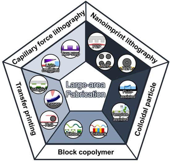
Figure 1. Schematic illustration of five main research directions of low-cost and scalable micro/nanofabrication.
While conventional methods such as focused ion beam milling (FIB), electron beam lithography (EBL), and photolithography have been widely adopted in commercial industries, they face challenges in terms of high production costs when dealing with structural scales below the micron level. So, various micro/nanofabrication have been explored to satisfy low-cost and high-throughput requirements for large-area submicron structure uniformity.
Soft lithography has emerged as a novel technology for fabricating or replicating submicron structure using elastomeric stamps, particularly with the use of polydimethylsiloxane (PDMS). Soft lithography is capable of patterning on flexible large-area substrates, facilitating high-throughput manufacturing with simple processes and low-cost organic/polymeric materials. Nanoimprinting lithography (NIL), transfer printing, and capillary force lithography (CFL) have been actively investigated as below.
NIL is a high-resolution patterning method that replicate desired patterns on a substrate using soft stamp. It is investigated for mass production with low-cost materials, mask-free processes, low manufacturing cost, and high production speed. The process involves curing the resist with ultraviolet (UV) or heat, using a stamp consisting of inverse patterns. NIL can be classified based on two aspects: resist curing and contact type. Also, it can fabricate uniform nanopatterns on various flexible substrate through a single-step process. Polymers used in NIL have wide applicability in optical/electronic devices such as 3D imaging, solar cells, light-emitting diodes (LEDs), and polarizers because of their ease of manufacturing and low reactivity. Various materials in NIL have expanded to other application fields, such as antireflective films, polarizers, solar cells, and metaholograms, demonstrating high resolution, scalability, productivity, and ease of use.
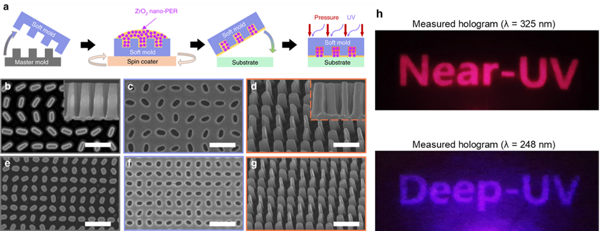
Figure 2. (a) Schematic of the NIL platform for fabrication of the UV metaholographic device. SEM images of (b) the master mold, (c) the soft mold, and (d) the imprinted metasurface of the target hologram designed for λ = 325 nm. (Inset) cross-section view. SEM images of (e) the master mold, (f) the soft mold, and (g) the imprinted metasurface of the target hologram designed for λ = 248 nm. All scale bars: 500 nm. (h) Measured images of the target hologram designed for λ = 325 nm (top) and λ = 248 nm (bottom).
Transfer printing is a technique used to assemble nanomaterials into functional arrangements by transferring patterns from a donor substrate to a target surface via a stamp. The process involves peeling-off and printing steps, and the stamp used is crucial for successful implementation. The method should consider interfacial adhesion, with adhesion strength and peeling velocity being important variables. When the fabrication parameters are well-defined, transfer printing exhibits uniformity, reproducibility, and scalability, which is required for integrating functional devices with flexible substrates. Three modified types of existing printing processes, including intaglio, laser-driven, and direct roll transfer printing, have been introduced among various types of transfer printing methods.
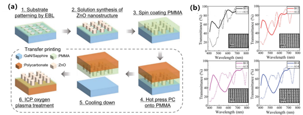
Figure 3. (a) Synthesizing and the transfer printing processes of ZnO nanostructures. (b) Transmittance spectra of as-grown nanorods array (A), and transferred nanorods array (B).
CFL is a technique that exploits capillary force to fill the void of the stamp to pattern complex nanostructures for photonic and electronic devices. CFL is one of several techniques developed to overcome the limitations of large-area fabrication of sub-micron structures. CFL has various practical applications in optical research due to its versatility. The reusability of stamps, compatibility with different large-area substrates, and easy molding have enabled the realization of complex structures, which has led to practical applications such as delivery systems and surface-enhanced Raman spectroscopy (SERS).
Colloidal particles, solid particles suspended in a fluid, are synthesized via several methods such as emulsion, dispersion, suspension, and Stöber method. Colloidal self-assembly is a process that colloidal particles are used to create well-arranged structures on a substrate. The process depends on the attractive or repulsive forces between the particles to form ordered structures. The structure can be controlled by adjusting various parameters, such as particle size/shape, as well as the properties of the solvent. The method has been used to create sub-wavelength photonic crystals.
By controlling certain parameters of the photonic crystal, such as periodicity, shape, and size, light with a certain wavelength range can be blocked. In addition, the refractive index in each direction can be varied depending on the periodicity of the photonic crystals in the spatial direction. Various methods of colloidal self-assembly have been developed, including spin-coating, convective self-assembly, Langmuir-Blodgett method, Marangoni effect, template-assisted method, and field-assisted method. The process is versatile and can be used with different materials, such as silica, polystyrene, and metals like gold and silver.
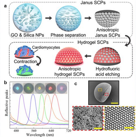
Figure 4. (a) Colloidal self-assembly processes for anisotropic Janus structural color particles (SCPs) by phase separation and cardiomyocyte monitoring platform. (b) Reflective peaks and reflection images of five different anisotropic Janus SCPs. (c) SEM images of whole (black line, scale bar is 100 μm), colorful hemispherical section (yellow line, scale bar is 1 μm) and black oblate section (red line, scale bar is 2 μm) of anisotropic Janus SCP.
BCP self-assembly is a process that two or more chemically distinct blocks are connected via linear covalent bonds. These blocks can have different chemical properties, such as solubility or reactivity. Using these properties, BCP spontaneously organizes into well-defined nanostructures when dissolved in a solvent. The self-assembly process is driven by the minimization of free energy, which leads to the formation of a range of structures such as spheres, cylinders, lamellae, and gyroids. The size/shape of these structures depend on the block length, the block ratio, and the solvent conditions. The precise control over the self-assembly enables the fabrication of complex structures with desired functions.
The resulting nanostructures have applications in a wide range of fields, including nanotechnology and materials science. To achieve high throughput, the fabricated substrate should be highly uniform. Various studies have been conducted on SERS substrates with high uniformity. A simpler evaporation method has been demonstrated using BCP self-assembly to obtain a hexagonal PS cylinder array enclosed by PMMA, followed by selective etching and gold deposition (Fig. 5). This method showed successful signal enhancement of the Raman spectra of the target, thiophenol, with a high uniformity of the nanogap distance and nanoparticle diameter. 


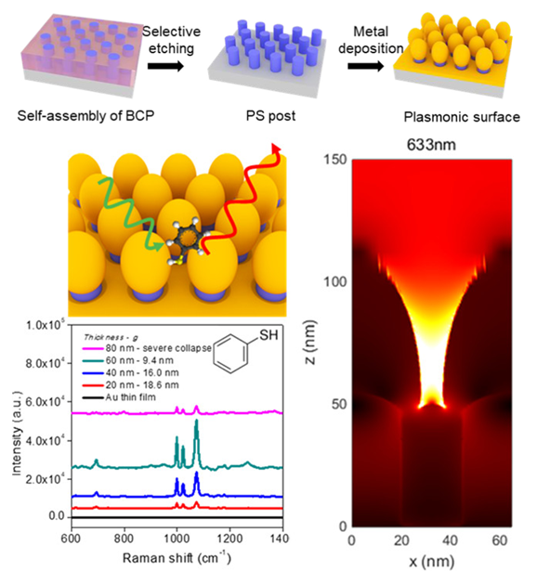
Figure 5. Ultralarge-area uniform plasmonic nanogap array formation via BCP self-assembly.
The review also presents whether silicon, TiO2, perovskite, etc. can be used in approaches mentioned in the manuscript. And their feature size/application are presented, providing a new perspective to keep readers up-to-date with the latest developments in the photonic fields.
In summary, the authors briefly discuss various sub-micron fabrication methods for a wide range of applications, focusing on the recent advancements in soft lithography and self-assembly techniques. Soft lithography and self-assembly techniques offer advantages, such as low-cost and high-throughput production of nanophotonic, which make them attractive for commercialization. However, these techniques also face several challenges such as limited material choices, sensitivity to environmental conditions, and limited feature sizes.
To realize their potential for commercial applications, engineering of optical materials, process optimization/standardization, and precise temperature control are necessary. Despite these challenges, soft lithography and self-assembly techniques hold great potential for commercialization of photonic devices. With these potentials, researchers should engineer advanced materials for obtaining the desired light-matter interaction at the target optical frequencies, improving the accuracy of nanofabrication techniques, and developing structures composed of multilayer stacks to overcome losses and fabrication difficulties.