
Jiangbing Du, Weihong Shen, Jiacheng Liu, Yufeng Chen, Xinyi Chen, Zuyuan He. Mode division multiplexing: from photonic integration to optical fiber transmission [Invited][J]. Chinese Optics Letters, 2021, 19(9): 091301
- Chinese Optics Letters
- Vol. 19, Issue 9, 091301 (2021)
Abstract
Keywords
1. Introduction
In a multimode optical waveguide, the light wave propagates in different paths, exhibiting different field distributions, so-called orthogonal modes. Optical field density can be significantly strengthened when multiple orthogonal modes are co-propagating in the same waveguide while maintaining acceptable or even improved performance of attenuation, dispersion, nonlinearity, signal quality, and so on. Such kinds of co-propagation of multiple orthogonal modes in one waveguide are called mode division multiplexing (MDM), which was first, to the best of our knowledge, brought up tens of years ago (as early as 1982[
1.1. “Moore’s law” for photonic integration
Photonic integration is a kind of microelectronic technology. However, it does not obey “Moore’s law” of conventional microelectronics, which has exponential development in the number of transistors per chip (100% increase per months). The basic reason is that the lightwave is at the micron-scale, which is much larger than electrons as well as electrical transistors. Meanwhile, the transmission and gating behavior of lightwaves are intrinsically different compared with electrons. Even so, quasi-“Moore’s law” development of photonic integration can still be observed due to the rapid development of photonic integration technologies (at their earlier stages), including silicon (Si) photonics (SIP), planar lightwave circuits (PLCs), III-V material integration, and so on.
From the historical view of microelectronics development, as presented in Fig. 1 (lower), “Moore’s law” has been well maintained (and is yet not dead) for continuously increasing the application specific integrated circuit (ASIC) integration density. Space division multiplexing (SDM) methods are also included in ASIC integration, which is well known as 2.5/three-dimensional (3D) stacking for packaging. The fabrication process is still developing and is now approaching 3 nm. Below 3 nm, the processes are getting more and more difficult. Therefore, SDM based on 2.5/3D stacking could play a very important role in maintaining “Moore’s law”.
Sign up for Chinese Optics Letters TOC. Get the latest issue of Chinese Optics Letters delivered right to you!Sign up now
![]()
Figure 1.Historical view of microelectronics development, PIC integration (upper), and ASIC integration (lower).
On the other hand, after more than three decades of development, photonic integrated circuit (PIC) integration is now stepping into the 28 nm process. However, most PIC integration platforms are still using the old fashioned process like 130 nm, 90 nm, and 45 nm, with balanced consideration of performance and cost. A very interesting situation is that improvement of process cannot lead to the steady improvement of integration density of PICs, which is limited by the intrinsic property of lightwaves. Then, inevitably, there will be a ceiling for PIC integration density, no matter how the advanced processes are utilized. Therefore, it is very difficult to realize large-scale photonic integration, and currently the largest amount of photonic components per chip is only about 850 by Massachusetts Institute of Technology (MIT)[
As shown in Fig. 1 (upper), the development of PICs (PLC, III-V, and SIP) will eventually step into SDM, just like ASICs. The difference is that photonic SDM is not just about 2.5/3D stacking. MDM can also be utilized here due to the intrinsic Boson property of lightwaves. The “Moore’s law” trend for photonic integration can thus be well maintained.
There are two different benefits for MDM in photonic integration: improved signaling density with more data in the same waveguide and improved efficiency with reduced power consumption for active devices. All of them are aimed at integration density. Together with 2.5/3D stacking and MDM, one can expect very a promising future for photonic integration. In this paper, we will talk about MDM out of photonic SDM.
1.2. “Moore’s law” for optical fiber transmission
As for optical fiber communication, more typically optical fiber transmission, the capacity crunch of the conventional single-mode fiber (SMF) is almost approached, based on the encouraging development of optical communication technologies in the past five decades[
Thus, 2020 is a special year, marking the end of a decade as well as the end for increasing trends of optical fiber transmission capacity based on the above-mentioned conventional technologies. The 50th anniversary of optical fibers also occurred in 2020, which brings up the new challenge of optical fiber transmission: what can we do to maintain the trend for the upcoming demand?
Presented in Fig. 2 are the historical trends of optical fiber transmission: the single-fiber capacity increases due to all kinds of technologies. Similar summarizations can also be found in Ref. [5] by D. J. Richardson et al. and Ref. [6] by T. Mizuno et al. The agreement for all of them is that SDM, including most importantly MDM, is the next answer for maintaining this “Moore’s law” trend of optical fiber transmission capacity.
![]()
Figure 2.Optical fiber transmission capacity trend with respect to all kinds of enabling technologies.
The current capacity record for standard SMFs (SSMFs) is 150.3 Tb/s[
Obviously, multi-core and MDM can be utilized simultaneously in SDM, but only MDM offers the intrinsic efficiency multiplexing of more data within the constraint space. Meanwhile, MDM is based on the few-mode fiber (FMF), which is more compatible with the SSMF system in terms of fabrication simplicity, cabling, maintenance, device, and so on. Therefore, we only focus on MDM out of SDM in this paper.
1.3. This paper
To make it clear, the key property of MDM is intrinsically the strengthened optical density in terms of signal transmission capacity, modulation efficiency, nonlinear efficiency, circuit size, and so on. Thus, MDM provides us with advantages for very broad and colorful applications, not only for optical communications, but also for imaging, endoscopy, spectroscopy, power combination, lasing, sensing, optical computing, and so on. In this review paper, we will talk about the perspective of optical communication, including, particularly, optical fiber transmission and photonic integration.
Versatile routes of MDM can be applied to different applications. As for photonic integration, TE/TM/transverse electromagnetic (TEM) MDM is currently the only solution due to the special waveguide structure. As for optical fiber transmission, linear polarization (LP) and orbital angular momentum (OAM) can both be utilized. LP MDM well utilizes the space of the optical fiber. It has good compatibility of fabrication, splicing with conventional SMFs. Meanwhile, its performances of attenuation, bending, nonlinear coefficient, dispersion, and so on are comparable with conventional SMFs. Generally speaking, LP MDM is a more natural upgrade solution with respect to the current SMF solution. OAM MDM is also an attractive solution with high scalability, which can be expected to be highly useful for the ultra-large capacity links. As for LP MDM, there is strongly coupled MDM and weakly coupled MDM. Currently, weakly coupled MDM is rather attractive for short reach applications, in which multiple-input multiple-output (MIMO)-less MDM for reduced cost and stable transmission for robust field applications is highly demanded. However, for long-haul optical transmission, strongly coupled MDM would be attractive, since reduced nonlinearity and reduced MIMO complexity can be expected.
This review paper consists of four sections. The background and motivation of MDM are introduced in Section 1. MDM photonic integration, including platforms, interface devices, passive devices, active devices, and so on, is presented in Section 2. In Section 3, MDM fibers, devices, and systems for large capacity optical fiber transmission are discussed. Section 4 is the conclusion, where the challenges and future trends of MDM for optical communications are discussed as well.
2. MDM Photonic Integration
2.1. Platforms for MDM photonic integration
This section will briefly introduce five material platforms for MDM photonic integration, including Si, Si nitride (SiN), chalcogenides, lithium niobite (LN), and indium phosphide (InP), and discuss the optical characteristics, fabrication process, and the recent works on MDM.
2.1.1. Silicon
Si is a mature photonic integration platform that has been widely used to pattern various passive and active devices for decades. The typical Si waveguide uses Si as the core material and Si dioxide () or air as the cladding. The refractive index of Si () is pretty high compared with air or the cladding layer, and hence strong optical guiding is guaranteed in the waveguide at the near-infrared wavelength. Besides, the strong optical confinement of Si allows for optical devices with a compact footprint. The Si-on-insulator (SOI) platform possesses plenty of advantages, including wide availability, low cost, and compatibility with mature complementary metal–oxide–semiconductor (CMOS) technology, which makes it one of the most prominent platforms for PICs.
The Si platform is suitable for MDM integration, as the propagation constant of the different spatial modes can be engineered to differ significantly thanks to the high core-cladding () index contrast. For the Si waveguide with a fixed thickness, one could continuously tune the propagation constant of the different spatial modes by varying the waveguide width. When the propagation constants of two closely placed waveguides match each other, the spatial mode will convert from one waveguide to the other. Various Si-based on-chip mode (de)multiplexers (MUXs) for MDM have been demonstrated in past years. Some typical structures of mode (de)MUX for MDM include multimode interferometers, asymmetric Y junctions, adiabatic couplers, and asymmetric directional couplers (ADCs)[
During the past decades, mode (de)MUXs for MDM on SOIs have been heading towards higher capacity and broader bandwidth. By introducing dual polarization to the mode (de)MUX, the number of mode channels can be increased up to 10[
2.1.2. Silicon nitride
SiN provides an alternative moderate-index-contrast system that is manufacturable in the CMOS environment[
For the SiN waveguide, is employed as the core layer and as the cladding material. The difference of refractive index values between core and cladding allows a compact structure of the optical waveguide. SiN has some unique advantages compared to Si. First of all, SiN has a transparency window over the range from 400 to 2350 nm, which is broader than Si (1100 to 3700 nm) and is very suitable for applications requiring shorter wavelengths (e.g., data communication at 850 nm). Besides, SOI-based photonic wires have typical waveguide losses of 1 to 2 dB/cm, mainly because of the low scattering loss originating from the sidewall roughness. For SiN waveguides, the propagation loss can be reduced down to an order of magnitude, typically in the range of 0.3–1.0 dB/cm. For nonlinear applications, SiN has the weaker Kerr nonlinearity than Si but the two-photon absorption (TPA) is virtually zero thanks to the material’s large bandgap. Therefore, it has been proved to be well suited for on-chip nonlinear progress, such as frequency comb generation or supercontinuum generation.
Compared with Si, fewer MDM works have been done on the SiN platform. In Ref. [19], a three-mode MDM-WDM circuit on a SiN-on-silica substrate using ADCs and a micro-ring resonator (MRR) was demonstrated and shown to be able to support a 30 Gb/s data transmission for each channel separately.
2.1.3. Chalcogenide
Chalcogenide glass (ChG) contains a major constituent of the chalcogen elements from group 6a of the periodic table (sulphur, selenium, and tellurium, but excluding oxygen), covalently bonded to network formers such as As, Ge, Sb, Ga, Si, or P. Employing a high refractive index of , ChG films for waveguide fabrication could be produced by thermal evaporation[
ChGs show promising application in various areas such as phase-change memories, solar cells, sensors, frequency conversion, and supercontinuum generation. The material nonlinearity of chalcogenides combined with the strong confinement and dispersion engineering achievable in the chalcogenide waveguide makes them attractive to form ultra-fast nonlinear devices. There are no free-carriers or TPA effects in chalcogenide materials. Meanwhile, these ChGs also have good mid-infrared transparency, thus supporting the applications like mid-infrared spectroscopy, which attracts growing interests because of its coverage over the characteristic spectral absorption features for many molecules. On-chip MDM interconnection at the 2 µm waveband was demonstrated on the ChG-on-dioxide platform, holding high-speed transmission[
2.1.4. Lithium niobate
The LN photonics platform has been an attractive platform over the past decades, due to its excellent material properties including the wide optical transparency window and high refractive index. Conventional LN waveguides are fabricated by titanium indiffusion or proton exchange, which typically form a low refractive index contrast[
However, etching of is a difficult task. Crystalline LN cannot be easily patterned due to its high chemical stability. As for traditional optical lithography, different hard masks such as hydrogen silsesquioxane (HSQ)[
LN has several excellent material properties including the large electro-optic (EO) modulation properties originating from the Pockels effect, the high second-order nonlinear susceptibility, and piezoelectric response, so that it was widely used to demonstrate various functionalities such as ultra-fast EO modulation, EO frequency comb, and second harmonic generation. As for the MDM application, Jin and co-workers demonstrated a mode switch based on the proton-exchanged LN waveguide, which can switch between the fundamental mode and higher-order mode with an extinction ratio of [
2.1.5. Indium phosphide
The most attractive characteristic of InP is its possibility to integrate passive and active devices (lasers, light amplifiers, modulators, and detectors) in a single membrane. A typical InP waveguide is formed on the InP-membrane-on-Si (IMOS). The thickness of the membrane is chosen in the range of 250–300 nm. InP has a high refractive index of 3.17, leading to compact photonic devices. The single-mode waveguide with the cross section of was commonly chosen.
The InP membrane can be bonded on a Si wafer through benzocyclobutene (BCB) adhesive polymer[
Due to the long-term development of InP material and devices, many passive devices used for MDM like a mode MUX and polarization converter have been demonstrated. For instance, a novel type of waveguide polarization converter that converts the mode to the mode with efficient mode conversion of 0.4 dB loss and 16.6 dB extinction ratio was demonstrated numerically[
A comprehensive comparison has been made in Table 1 regarding these fiber photonic integration platforms.
| SOI | SiN | ChG | LN | InP | |
|---|---|---|---|---|---|
| Index | 3.4 | 2.0 | 2–3 | 2.6 | 3.2 |
| Loss (dB/cm) | 0.1 | 0.05 | 0.027 | 0.3 | |
| Window (µm) | 1.1–3.7 | 0.4–2.4 | 1.5–12 | 0.4–5 | 1.3, 1.5 |
| Lasing | No | No | No | No | Yes |
| PD | Yes | No | No | No | Yes |
| Modulation | Yes | No | No | Yes | Yes |
| Extra doping | / | / | Standard process | Standard process | |
| CMOS compatibility | Yes | Yes | No | No | No |
Table 1. Photonic Integration Platforms
2.2. MDM interface for PIC-fiber coupling
Interface coupling builds an indispensable bridge that connects the optical signal from integrated waveguides to fiber transmission. The chip-to-fiber coupler can typically be classified into two types, vertical grating coupler (GC) and edge coupler, which have their own merits and have already been well investigated in the last decades. However, when it comes to multimode coupling, it becomes more complicated to maintain all of the guided modes having high coupling efficiency. In this section, we review the recent works on multimode interfaces for coupling between multimode waveguides on PICs and FMFs, as depicted in Fig. 3. Their practical application for an MDM transponder is also discussed. The summary of some typical MDM interfaces on SOI is listed in Table 2.
| Properties | Vertical Coupling | Edge Coupling | |
|---|---|---|---|
| Ref. [ | Ref. [ | Ref. [ | |
| Mode number | 6 | 4 | 2 |
| Coupling loss | 20–25 dB | 4.9–6.1 dB | 10.77 dB |
| Crosstalk | / | −7.3 to −11.9 dB | |
| Bandwidth | 20 nm | ||
| Footprint/length | mm-scale | ||
Table 2. Cutting-Edge Performance of MDM Interface on SOI
![]()
Figure 3.Schematic diagram of MDM optical interface, including vertical coupling with on-chip mode multiplexer (MUX) and edge coupling with 3D asymmetric waveguide. (i)–(iii) Specific progresses of the MDM interface[
2.2.1. Grating coupler
As for the GC for higher-order mode coupling in FMFs, a straightforward method is to multiply the number of GCs so that each GC can correspondingly emit each lobe in the high-order mode (HOM). For instance, a double-part GC was employed to convert the mode in the waveguide into the mode in the FMF, with a peak coupling efficiency of [
In order to support multimode coupling, Koonen et al. proposed a Si PIC mode MUX with five parts of two-dimensional (2D) GC, which can support six polarization modes (, , , , , ) excited from the PIC to FMF[
Another scheme is using a single GC to selectively launch several modes with high efficiency. Tong et al. demonstrated a novel multimode GC by genetic optimization, supporting four LP modes (, , , ) with low coupling loss of 4.9 dB for and 6.1 dB for [
2.2.2. Edge coupler
Generally, the edge coupler is based on the inverse taper waveguide leaking the optical field into the cladding layer with a larger field diameter so as to decrease the mode mismatch between integrated waveguide and Si fiber. As for HOMs, e.g., , we can adopt the edge coupler with two individual inverse tapers to match the two lobes of the mode field[
In Ref. [47], a multi-stage SOI inverse taper buried in SiN cladding was designed to excite six polarization modes in the FMF, whereas the mode hybridization needs a pretty large length of 2.3 mm in total, which is impractical. Different from the highly compact Si PIC, a polymer material has a similar refractive index with the Si fiber, so that it is quite easy for polymer waveguides to transfer the guided modes into the FMF and also to fabricate a multi-layer structure to support vertical HOMs. In Ref. [48], a polymer multimode edge coupler based on 3D asymmetric waveguide branches was proposed for four modes (, , , ) with a small coupling loss of for all four modes despite the large mode converter (MC) loss in the polymer device. Thus, a polymer may be more suitable for multimode edge coupling between integrated waveguides and the FMF, but not better than Si devices for MCs.
2.3. Passive devices
Passive devices constitute a significant foundation in MDM photonic integrated systems for the mode multiplexing/demultiplexing and the propagation and routing of multimode signals. This section will introduce recent researches on multimode waveguiding devices, power coupling devices, and mode and wavelength manipulating devices, mainly focusing on the SOI platform. Multimode passive devices with small size, low loss, low modal crosstalk, and high scalability are mainly discussed.
2.3.1. Waveguide devices: bend and crossing
Generally, in a standard Si layer with 220 nm thickness, a 500-nm-wide single-mode waveguide can be bent by a 10 µm radius with negligible bending loss. While for a multimode waveguide, it is far more sensitive to the bend due to the much wider mode field. There will be extra scattering loss since the leakage into the cladding at the bending area will be severely affected by the sidewall roughness. Therefore, a multimode bent waveguide with a smaller bending radius under acceptable low bending loss is quite important for a dense MDM integrated system. Here, we introduce three kinds of multimode waveguide bends for MDM photonic integration. The benchmark performances of different MDM bends are summarized in Table 3.
| Properties | Euler Bend[ | SWG Bend[ | Pixelated Bend[ |
|---|---|---|---|
| Structure and principle | Waveguide curve optimization | SWG for mode converting | Inverse design of pixelated structure |
| Mode number | 4 TM modes | 6 modes with dual polarizations | 4 TE modes |
| Bending radius | 45 µm | 10 µm | 3.9 µm |
| Loss | |||
| Crosstalk | |||
| Scalability | Yes | Yes | Yes |
Table 3. Benchmark Performance of MDM Bend
The first one is based on the optimized curve, for instance, the Euler bend with a 45 µm effective radius for four TM modes and bending loss[
![]()
Figure 4.Schematic diagram of integrated multimode waveguide bends: (a) the Euler curved bend for four TM modes[
The second one is to introduce an MC before and after the bent waveguide in order to match the mode field in the straight waveguide and bent waveguide, like the subwavelength grating-based MC in Ref. [53]. Besides, a compact bent waveguide with 10 µm radius including MC length was applied for two TE modes with loss and crosstalk[
Thirdly, in recent years, inverse design has become a novel design method for PIC devices, in virtue of the ability to break the conventional design frame and automatically obtain the optimized devices with outstanding performance and compact footprint. Ultra-compact multimode bent waveguides can be optimized based on pixelated meta-structures, with a 3.6 µm radius and loss for two TE modes[
Furthermore, inspired by the on-chip-geometrical-optics configuration, a novel four-mode bend based on a total-internal-reflection (TIR) mirror was reported in Ref. [56], as shown in Fig. 4(d). The same concept was also used for the MDM crossing, 3 dB coupler, and switch, with easy design and scalability to much larger mode numbers. However, these four-mode devices are constituted by a 10-µm-wide waveguide, which still needs a long adiabatic taper to match with normal four-mode waveguides.
Crossing is another basic component in high-density MDM networks. Seeing that the conventional single-mode waveguide crossing is typically based on the self-imaging of multimode interference (MMI), the multimode waveguide crossing can be designed by the same principle. Dual-mode crossing was proposed by optimizing the joint self-images of two TM modes[
![]()
Figure 5.Schematic diagram of integrated multimode waveguide crossing: (a) two-mode crossing based on non-adiabatic tapered waveguide[
2.3.2. Power coupling devices
In an MDM photonic integrated system, a power splitter is the basic component to allocate the power distribution of multimode signals in different channels. A dual-mode 3 dB power splitter was designed by a straightforward structure[
2.3.3. Mode manipulation devices: MUX/deMUX/mode converter/exchange/filter
Mode MUXs/deMUXs are the most significant devices in MDM systems, where they convert the different channels of the fundamental mode to HOMs, combine them together in multimode waveguide channels, and finally reconvert the HOMs to fundamental modes and separate into the original channels. For photonic integrated MDM systems, mode MUXs/deMUXs have already attracted plenty of researches in recent decades. Till now, the structure of the mode MUX/deMUX can be classified into plenty of types, such as MMI[
| Ref. | Year | BW (nm) | Channel | Structure | E / S | |||
|---|---|---|---|---|---|---|---|---|
| [ | 2012 | 80 | 1 | 50 | 2 (TE) | MMI + PS | S | |
| [ | 2014 | 48.8 | 0.3 | 100 | 2 (TE) | Symmetric Y junction + PS + MMI | S | |
| [ | 2020 | 7.24 | 0.74–1.2 | 50 | 2 (TE) | Shallow-etched MMI | E | |
| [ | 2013 | 50 | 0.3 | 100 | 2 (TE) | Adiabatic tapered ADC | E | |
| [ | 2016 | 68 | 0.8–1.3 | 65 | 2 (TE) | Taper-etched ADC | E | |
| [ | 2018 | 15–50 | 0.2–1.8 | −15 to −25 | 90 | 10 (PM) | Adiabatic tapered ADC | E |
| [ | 2019 | 75 | 1.5 | / | 75 | 12 (TE) | Adiabatic ADC using SWG | E |
| [ | 2013 | 1.5 | 100 | 2 (TE) | Asymmetric Y junction | E | ||
| [ | 2016 | 510 | 5.7 | −9.7 to −31.5 | 29 | 3 (TE) | Cascaded asymmetric Y junction | E |
| [ | 2013 | 300 | 0.3 | 100 | 2 (TE) | Adiabatic coupler | E | |
| [ | 2016 | 200 | 1 | 75 | 2 (TE) | Adiabatic coupler + Y junction | E | |
| [ | 2017 | 180 | 1.5 | 90 | 2 (TE) | Adiabatic coupler + Y junction | E | |
| [ | 2014 | 25 | 3–16 | −12 to −22 | / | 3 (TE) | Micro-ring | E |
| [ | 2015 | 100 | 1.5–3.5 | −20 to −32 | / | 3 (TE) | Micro-ring | E |
| [ | 2019 | 40 | 2.1 | / | 4 (TE) | Micro-ring | E | |
| [ | 2013 | 90–250 | 0.2–0.34 | −22 to −30 | 3.7–11.8 | 4 (TE) | Grating-assisted contra-DC | S |
| [ | 2015 | / | / | / | 2 (TE) | Grating-assisted tapered contra-DC | E | |
| [ | 2020 | 300 | 6.6 | 4 (PM) | SWG-based contra-DC | E | ||
| [ | 2016 | 1.2 | 100 | 2 (TE) | Topology optimized structure | E | ||
| [ | 2018 | 1.2–2.5 | 60 | 3 (TE) | Pixelated structure | E | ||
| [ | 2020 | 1.5 | 60 | 4 (TE) | Pixelated structure | E | ||
| [ | 2018 | 4 | 40 | 2 (TE) | Triple waveguide coupler | E | ||
| [ | 2018 | 7.5 | 0.32 | 35 | 2 (TM) | Triple waveguide coupler with hybrid plasmonic waveguide | S |
Table 4. The Summary of Mode MUX/deMUX
First, the MMI-based mode MUX typically presents wide bandwidth and high tolerance to fabrication errors with a long size and becomes complicated for HOMs greater than the second one. However, an asymmetric shallow-etched MMI was reported as a two-mode MUX with a footprint of [
![]()
Figure 6.Schematic diagram of integrated mode MUX/deMUX: (a) 10-channel mode (de)MUX with dual polarizations by adiabatic tapered ADC[
Besides the mode MUX/deMUX, the MC[
![]()
Figure 7.Schematic diagram of universal (a) MC[
2.3.4. Wavelength/polarization manipulation devices: filter/polarization splitter/rotator
As we reviewed before, passive multimode devices constitute the foundation of the integrated MDM system. At the same time, some multimode devices are capable of wavelength/polarization manipulation as well. For instance, ADC-based mode conversion can drop certain polarization modes so as to obtain the polarization splitter. Based on such a principle, a polarization beam splitter (PBS) was reported in Ref. [102], in which the mode is dropped down from by converting into the mode through ADC-based mode MUX and then coupling back to through another ADC, as shown in Fig. 8(a). Besides, another PBS was composed by an ADC-based mode MUX and multimode asymmetric sidewall Bragg grating[
![]()
Figure 8.Schematic diagram of (a), (b) integrated PBS based on mode conversion[
As mentioned before, inspired by an on-chip-geometrical-optics configuration, multimode bend, crossing, 3 dB coupler, and switch were demonstrated by a TIR mirror, which provides a brand-new concept for designing multimode devices. Besides, the TIR mirror was also applied to realize a mode-transparent PBS in a wide multimode waveguide, as depicted in Fig. 8(c). PBSs for 13 modes, including six TE modes and five TM modes, were demonstrated with low insertion loss and low modal/polarization crosstalk[
2.4. Active devices
2.4.1. Modulator
In the MDM photonic integration system, different spatial modes should be sent into different modulators separately and then combined by mode MUX for MDM transmission. Here, each mode is treated as an independent channel and modulated by an independent electric signal. As a result, there is not any multimode modulator that supports the multimode transmission and EO modulation at the same time. However, the working principle of MDM could also be utilized in the integrated modulator to improve the performance in size and modulation efficiency. For instance, in Ref. [111], Zhou et al. demonstrated a Si-based modulator, which was composed of the multimode waveguide as phase shifter, as shown in Fig. 9(a). Different from the traditional Mach–Zehnder interferometer (MZI), this type of phase shifter has only one arm. Two branches of light travel as different spatial modes, and , and finally interfere with each other at the output port. This type of modulator reduces one arm in the MZI interferometer, thus reducing the optical device size by half. On-off keying modulation was demonstrated with extinction ratio of 5.5 dB at 32 Gb/s. Besides, the orthogonality among different spatial modes allows them to share one physical channel simultaneously.
![]()
Figure 9.Schematic diagram of (a) Si-based MZI modulator with two branches of light propagating in one multimode waveguide[
Reference [113] shows that different spatial modes could go through one phase shifter successively, thus increasing the effective optical length. As shown in Fig. 9(b), the thermal-optic phase shifter consists of a multimode waveguide and several MCs based on the DC structure. In the recycling structure, light is input as the mode at first, then converts into the mode via two mode MUXs at the end of the phase shifter, and is sent back to the bus waveguide in the opposite direction. After going through the phase shifter two times, it is then converted to the mode and sent back to the bus waveguide in the forward direction. By recycling the light in the bus waveguide for times, the phase change enlarges times accordingly. The thermo-optic phase shifter finally realized the power consumption of 1.7 mW per , which is more than an eight-time reduction compared with the traditional MZI structure. Notably, the light recycling scheme makes a difference on the phase shifter based on the thermo-optic effect; that is because the efficiency of thermal tuning for HOMs does not decrease as the waveguide grows wider, while totally differing from the multimode phase shifter based on the carrier dispersion effect. The low-energy phase shifter makes a great difference for the optical phased array and Lidar applications, which will be discussed in the next section.
2.4.2. Switch
Different from the MC, which is used to convert spatial modes to each other, a typical mode switch should be able to support data exchange between any two spatial modes that carry different transmission data. In Ref. [114], a simple MC can be realized by combining two uniform MCs together, as shown in Fig. 10(a). Two micro-ring-based MCs that convert the mode to the mode were combined. When the input is the mode, it will go through the MRR1, couple in MRR2, and then convert to the mode. Similarly, when the input is the mode, it will couple in MRR1, convert to the mode, and then go through MRR2. In Ref. [115], a reconfigurable mode switch based on the MZI structure was proposed by Sun et al. The schematic of the proposed structure is shown in Fig. 10(b); the whole structure consists of two symmetric Y junctions and a phase shifter. The input mode will evolve first into an even super-mode and then split to two branches with uniform optical phase. Similarly, the input mode will evolve into an odd super-mode and then split to two branches with opposite optical phases. When the state of the switch is OFF, the two branches of light will arrive at the output port without any change. When the state of the switch is ON, the upper branch of light will be induced to a shift, and thus the output mode will be changed.
![]()
Figure 10.Schematic of (a) mode switch based on two micro-rings[
A similar concept was also used for high-speed two-mode switches based on a Y junction, phase shifter, and MMI[
2.5. MDM circuits and subsystems
Based on the fundamental passive multimode devices introduced above, large-scale MDM circuits and subsystems can be built for various functions, like switching and routing. Besides, other functional devices or systems can also be innovated by means of the concept of MDM with high-efficiency spatial utilization, for instance, the optical phased array. In this section, we will list some large-scale reconfigurable optical integrated MDM systems for switching, routing, and even phase controlling and discuss their prospect and challenges.
2.5.1. MDM for optical phased array
Optical phased array provides a prospective solution for beam-steering applications in ultra-small solid-state Lidar and free-space communication systems. For the large-scale optical phased array, power consumption is an intractable problem, since the thermal-optic phase shifter typically consumes tens of milliwatts of power and results in an overall power consumption of hundreds of watts. To solve that problem, Miller et al. demonstrated a high-efficiency large-scale Si integrated optical phased array using an MDM-based multi-pass phase shifter, as shown in Fig. 11, totally containing 512 actively controlled elements and consuming only 1.9 W of power while performing 2D beam steering over a field of view[
![]()
Figure 11.Schematic diagram of Si optical phased array based on multi-pass recycling structure by mode multiplexing[
2.5.2. MDM interconnect system (hybrid with WDM/PDM)
Multiplexing technology can generate tens or even hundreds of times of increased capacity of the overall interconnect system, especially by hybrid multiplexing of wavelength, space (mode), and polarization domains. In order to actualize hybrid multiplexing, MDM devices have to present broadband operation to satisfy as many wavelength channels as possible. Figure 12 illustrates the scheme of hybrid multiplexing, in which all of the elements except for the wavelength MUX have broadband operation containing the wavelength range of WDM. The WDM channels are combined by wavelength MUX, then split, and modulated to form MDM/PDM channels via the PR and mode MUX. The hybrid signals propagate in the multimode waveguide and are de-multiplexed in the reverse process. As a realized demonstration, 12 hybrid multiplexed channels () were reported on the MDM circuit by micro-ring-based mode MUX, with a single-channel speed of 10 Gb/s[
![]()
Figure 12.Schematic diagram of integrated interconnect system hybrid multiplexed by WDM, MDM, and PDM.
2.5.3. MDM switch network/ROADM system
Optical switching and reconfigurable optical add-drop multiplexing (ROADM) are vital functionalities for optical interconnect networks. Multiplexing technology like MDM and WDM increases the density and capacity of optical networks, while also bringing in the challenge of switching and ROADM. In recent years, reconfigurable switch arrays and ROADM for hybrid multiplexing systems have been investigated in various schemes. The majority of them are based on MUX/deMUX and conventional single-mode switching units, that is to say, the multiplexed signals of each path are firstly demultiplexed into individual channels, then arrays of switching units selectively route the signals among different channels and paths, and finally the reconfigured channels are again multiplexed into HOMs in original paths and output. The schematic process is illustrated in Fig. 13(a). For instance, Jia et al. reported the WDM-compatible multimode switching circuits with all the optical network on-chip except for the WDM source[
![]()
Figure 13.Schematic diagram of on-chip switching networks ROADM for multiplexing: (a) on-chip typical multimode optical switching system[
3. Large Capacity MDM Optical Fiber Transmission
3.1. FMF fibers
The FMF is the basic and essential part in MDM systems to enlarge the total capacity of fiber optic communication systems. Due to the modal coupling among different modes, MIMO is applied to recover signals that have been degraded during the FMF transmission and mode MUX/deMUX[
3.1.1. Conventional FMF for MIMO-less MDM
The complexity of MIMO processing is mainly caused by large mode crosstalk and differential mode group delay (DMGD). Here, we introduce two kinds of FMFs to reduce mode crosstalk for MIMO-less MDM systems.
Firstly, step index fibers with a standard structure are proposed to reduce mode coupling by enlarging the effective index () between mode groups. For instance, a four-LP-mode FMF with differences , differential group delays (DGDs) of 1–9 ps/m, of , mode-average loss , and integrated crosstalk of was designed, which can be used for three-mode transmission at 100 Gb/s over 40 km[
![]()
Figure 14.(a) Optimized step-index profiles of different FMFs[
The second one is ring-assisted fibers with a multi-layer circle core and annular index structure providing more freedoms to enlarge . Jiang et al.[
Thanks to these two fibers with lower mode coupling, the complex MIMO processing can be replaced by several simple local MIMO, eventually approaching MIMO-less. Besides, it is also desirable to simplify decoding complexity by lower DMGD, which compensates mode-coupling at the receiver side. In view of that, as seen from Fig. 15(a), Sato et al. fabricated a two-mode graded-index fiber with and , which has a large effective area of for the mode and approximately 0.016 dB/km bending loss for the mode at , and it realized differential mode delay (DMD) of including zero in the C-band[
![]()
Figure 15.(a) Refractive index profile of two-mode graded-index fiber[
Another method to simplify or eliminate MIMO processing is employing elliptical core fibers by dividing different modes in the same degenerate mode group. This fiber is widely applied to a polarization-maintaining fiber (PMF), acousto-optic frequency shifters[
Furthermore, in recent years, multi-core super-mode fibers have been proposed as one of the important methods to increase the transmission capacity of long-distance MDM systems. Super-mode fibers can achieve higher mode density, higher design freedom, no mode-related loss, and larger effective area than single-core FMFs[
![]()
Figure 16.Schematic of a multi-core super-mode fiber[
3.1.2. Inverse design of FMF fiber
Conventional FMFs are based on sweeping the structure parameters to meet different characteristic requirements, which is time-consuming. Recently, an inverse design using neural network (NN) has been proposed with high accuracy, high efficiency, and low complexity for a fast and reusable design of optical fibers.
As shown in Fig. 17(a), the entire design process can be divided into two modules, forward design and inverse design. Forward design is utilized to generate a data set in different structure parameters by software simulation (like Lumerical or COMSOL). The inverse design process using NN is to automatically establish the mapping between the input and output from forward design by adjusting the weight of different layers and reducing error values. This inverse method is firstly used to design a weakly coupled fiber with a multi-ring structure supporting more modes. In Ref. [145], a sequential model with three hidden layers, where each layer has 300 neurons, was constructed to predict structure parameters of four-ring fibers supporting four modes with distribution meeting the weakly coupled objective. By comparing simulated by predicted parameters and target , the correlation of for all modes is above 0.99, and relative errors are below 0.0025%. In this way, we have successfully designed an FMF structure with a little larger maximum in the initial data set. This proposed method will play an important role in the inverse design of other kinds of FMFs thanks to its good accuracy and low complexity.
![]()
Figure 17.(a) Flow chart of the proposed NN-assisted inverse design method. (b) The inverse design frame of the NN[
3.2. MDM MUX/deMUX
In MDM fiber optic transmission systems, the transmitter generates multiple channels of fundamental mode into SMFs carrying different signals. In order to utilize the modes of FMF as independent channels, the signals of the mode need to be converted into higher-order modes and then multiplexed into the FMF. At the receiver, the multiplexed signals also need to be demultiplexed and then processed separately. Therefore, the MC and MUX are the fundamental devices in MDM systems. In particular, the MC and MUX are always realized by a single device, and we call it a mode MUX. Here, we introduce two main types of mode MUXs in fiber MDM systems: free-space beam MUX and all-fiber MUX.
3.2.1. Free-space beam multiplexer
Free-space beam MUXs change the optical field distribution of the fundamental mode to that of a higher-order mode by using a spatial light modulator (SLM)[
![]()
Figure 18.Schematic diagram of mode MUX based on free-space beam combiner[
3.2.2. All-fiber multiplexer
Since free-space beam MUXs use lenses to couple the light into the fiber, the coupling efficiency is quite low. In order to realize high coupling efficiency between MUXs and fibers, all-fiber MUXs are developed. There are three types of all-fiber MUXs: directional fiber coupler, long-period fiber Bragg grating (LPFBG) structure, and photonic lantern.
The directional fiber coupler can be achieved by a mode-selective coupler (MSC), which consists of one FMF arm and one SMF arm, as shown in Fig. 19[
![]()
Figure 19.Directional fiber-coupler-based (a) mode MUX and (b) mode deMUX supporting
LPFBG-based MUXs use LPFBG to realize mode conversion and use an FMF coupler to achieve multiplexing[
![]()
Figure 20.LPFBG-based (a) mode MUX and (b) mode deMUX supporting
The two types of all-fiber MUXs from above achieve high coupling efficiency, but they lack flexibility. If the number of channels is increased, we need to add corresponding couplers into the MUX. Moreover, different modes are multiplexed or demultiplexed in order from the fundamental mode to the high-order mode. These disadvantages make it inconvenient for system building. Therefore, photonic lanterns attract the attention of researchers.
Photonic lanterns are an optical waveguide coupling light from several SMFs to one multimode fiber (MMF)[
![]()
Figure 21.Schematic diagram of a photonics lantern[
3.3. MDM amplifiers
In MDM transmission systems, amplifiers are a particularly important device due to the function of compensating the signal attenuation of fibers. Compared with amplifiers in SMF systems, besides conventional parameters of amplifiers such as gain and noise figure, we should also focus on the supporting modes and mode dependent gain (MDG) of MDM amplifiers. In MDM systems, the power difference of each mode should be controlled to be a low level, otherwise transmission performance will be reduced. Therefore, for MDM amplifiers, the gain difference between all modes, called MDG, must be small. Few-mode (FM) EDFAs and FM distributed Raman amplifiers (DRAs) are two widely adopted solutions, and they are developed from corresponding SMF amplifiers.
3.3.1. Few-mode erbium-doped fiber amplifiers
EDFAs are the conventional solution for light amplification in optical transmission systems, and they also can be extended into MDM systems. The main properties of FM-EDFAs are focused on the number of supporting modes, gain, MDG, noise figure, and so on. As single-mode EDFA has been extensively investigated, and the researches of FM-EDFAs are concentrated on the refractive index profiles and erbium doping profiles, which are effective solutions to reduce MDG.
The first proposed scheme is the design of erbium doping profiles. Jung fabricated a two-mode EDFA supporting and modes for the first time, to the best of our knowledge[
![]()
Figure 22.(a) Ring-shaped erbium doping profile[
Precise distribution of the refractive index and erbium doping needs complex crafts, which makes the fabrication of erbium-doped fibers (EDFs) rather difficult. For solving this problem, an FM-EDF micro-structured with inclusions was reported[
3.3.2. Few-mode distributed Raman amplifiers
In MDM systems, as multi-channel signals are multiplexed and propagated together in the FMF, the power density will be much higher compared with SMFs, which lead to more serious nonlinear distortion. Moreover, crosstalk among different modes degrades the SNR of signals. In order to make full use of the limited bandwidth, advanced modulation formats, such as QAM, have been extensively investigated for increasing the spectral efficiency in SMF transmission systems[
![]()
Figure 23.Schematic principle of DRA for mitigating the nonlinear distortion and noise over EDFA[
DRAs utilize stimulated Raman scattering to transfer the power from the pump to signal. DRA has many advantages compared with EDFAs. DRAs have higher SNR and less nonlinear distortion, as Fig. 23 displays. Moreover, DRAs have flexible gain profiles and bandwidth, which can be adjusted according to the demand by controlling the pump wavelength and power. MDG of FM-DRAs can also be controlled by customizing the pump component. Taking advantage of this merit, we can maintain the MDG of amplifiers at a low level or customize the MDG of amplifiers to compensate the MDL of the whole system. Finally, from the perspective of fabrication, DRAs only need several pump sources, while the manufacturing of EDFAs requires erbium doping according to a specific profile and drawing.
Ryf for the first time, to the best of our knowledge, demonstrated a backward FM-DRA supporting two modes[
DRAs for SMF systems have been widely investigated, and many novel structures are proposed to improve the performance. High-order Raman pumps can effectively improve the noise figure, thus being induced into MDM systems, with 1.8 dB improvement of amplified spontaneous emission (ASE) noise[
![]()
Figure 24.Quasi-lossless transmission with bidirectional high-order pump[
For MDM systems, two algorithms for designing the FM-DRAs based on bidirectional pumping random fiber lasers were proposed. One of them was particle swarm optimization (PSO) for time, wavelength, and mode equalized FM-DRAs, which utilized four first-order pumps and one second-order pump[
![]()
Figure 25.Inverse design based on NN for FM-DRA[
3.4. MDM transmission experiments and progresses
The research of MDM fiber transmission can be traced back to 1982 when two modes were transmitted over a 10 m MMF[
Current researches of MDM systems are mainly concentrated on the achievement of higher capacity and longer distance. The extension of capacity mainly depends on the number of channels, which is realized by increasing SDM channels and combining multiple hybrid multiplexing technologies such as WDM and PDM[
Compared with SMF systems, MDM technology induced MDL and DMD, which negatively affect the transmission distance. Rademacher demonstrated long-distance MDM transmission in three-mode fibers over 3500 km and gave the analysis of MDL that fundamentally limits the transmission reach[
Figure 26 presents recent MDM experiments and progresses. Currently, large capacity and long distance are difficult to achieve at the same time, as large capacity demands more space modes but also induces MDL and DMD, which negatively influence the received signal. To further improve MDM systems for high capacity and long distance, besides developing the devices supporting more modes, MDL and DMD of MMFs are significant problems to be improved.
![]()
Figure 26.Recent-year MDM experiments and progresses.
4. Conclusion
In this paper, we review the cutting-edge progresses of MDM technology for the scenerios from photonic integrated interconnection to optical fiber communication. Achievements of passive and active devices and MDM systems are summed up and discussed.
For MDM photonic integration, we give a review of integrated platforms, multimode interfaces for chip-to-fiber coupling, multimode passive devices (including bends, crossings, power splitters, mode MUXs, and so on), multimode active devices like switches, and MDM circuits and subsystems. Till now, the highest number of on-chip MDM channels is realized by SWG-based ADC, supporting 12 TE modes multiplexed in one single multimode waveguide. The challenge for further higher-order mode multiplexing will be how to relax the fabrication tolerance of coupling efficiency as mode order increases. However, other multimode passive devices, like multimode interfaces, bends, and crossings, still have difficulty supporting more than six modes with high performances. These devices with higher-order mode operation, lower insertion loss, more compact footprint, and even more universal for design are the crucial trends for the future research. Besides, MDM switching networks with optimized routing architecture and compactness for more mode channels are the key challenges to realize large-scale MDM on-chip interconnection. For currently achievable MDM supporting 2–6 modes, hybrid multiplexing with WDM is a reliable method to enhance the total capacity of photonic integrated interconnection and also a long-term trend for on-chip multiplexing. Furthermore, in order to make the bridge between on-chip multimode signals and modes propagating in FMFs, multimode interfaces with low coupling loss and higher reliability are still a big challenge for practical implementation. One cannot use too many modes in a single waveguide for high-density MDM. There are several reasons. One reason is the increased waveguide size, which limits the dense integration and increased fabrication complexity, and bending loss will also be induced. Another reason is the nonlinear distortion due to TPA and Kerr nonlinearity. Si has a high index with a high nonlinear coefficient, which makes Kerr nonlinearity a big issue. At 850 nm, or even O band and C band, TPA is still a problem, which leads to increased loss and noise. One more consideration is the optical interface between MDM PIC and FMF, which typically supports very few modes, like two-mode MDM.
For MDM optical fiber transmission, we review the progresses of FMFs, mode MUXs based on fiber structure, fiber amplifiers for FM systems, and MDM fiber transmission links. We introduced the novel inverse design method for weakly coupled FMFs with high accuracy, high efficiency, and low complexity for fast and reusable fiber designs. Fiber-based mode MUXs, like MSC, LPFBG, and photonic lanterns, provide high efficiency for mode multiplexing, while the fabrication process may be difficult for massive production. FM amplifiers play an essential role for long-haul MDM transmission. DRAs show the advantages of maintaining the MDG for each mode, providing more flexible and customizable designs for FM amplification. Finally, MDM transmission with larger capacity and longer distance is the main target all the time. Key fiber devices reviewed above eventually promote the transmission performances of the whole MDM system. MDM combined with multi-core fibers and WDM shows powerful prospects for next-generation fiber communication with ultra-high capacity.
The implementation requirements need to be considered for MDM in order to make it practical for field applications. As for photonic integration, the on-chip process is rather stable, and MDM devices are quite reliable based on the standard fabrication. The key problem would be the limitation of the optical interface between the PIC and optical fiber, where significant mismatch can be expected between TE/TM modes in the photonic waveguide and LP modes in the fiber. As for optical transmission, MDM can be applied in two scenarios, including brand-new transmission systems with everything compatible with MDM and subsystems like EDFA with SMF input and output but with highly efficient MDM amplification inside. Due to the stability issue, MDM for optical transmission would be challenging, and short reach applications with weak coupling fibers for MIMO-less interconnection are currently more practical. Generally, one can expect practical applications of MDM for transceivers and active optical cables based on PIC and weak coupling FMFs and amplifier subsystems based on FM-EDFs.
To conclude, MDM technology shows a dominant position to overcome the capacity crunch of optical communications, no matter for chip-scale or short-reach interconnection or long-haul transmission. There are still some challenges for MDM devices and systems (for integrated photonics or fiber optics) to achieve more reliable properties. The core problem includes but is not limited to the methodologies to increase the mode channels and reduce the system cost per channel, improving the compatibility between single-mode and MDM systems at the same time. Further heroic researches and achievements are expectant to be made in the future to lead this area for maintaining the “Moore’s law” trend of optical communication.
References
[1] S. Berdagué, P. Facq. Mode division multiplexing in optical fibers. Appl. Opt., 21, 1950(1982).
[2] C. Sun, M. Wade, Y. Lee, J. S. Orcutt, L. Alloatti, M. S. Georgas, A. S. Waterman, J. M. Shainline, R. R. Avizienis, S. Lin, B. R. Moss, R. Kumar, F. Pavanello, A. H. Atabaki, H. M. Cook, A. J. Ou, J. C. Leu, Y.-H. Chen, K. Asanović, R. J. Ram, M. A. Popović, V. M. Stojanović. Single-chip microprocessor that communicates directly using light. Nature, 528, 534(2015).
[3] S. C. Gupta. Textbook on Optical fiber Communication and Its Applications(2018).
[4] P. J. Winzer. Scaling optical fiber networks: challenges and solutions. Opt. Photon. News, 26, 28(2015).
[5] D. Richardson, J. Fini, L. Nelson. Space-division multiplexing in optical fibres. Nat. Photon., 7, 354(2013).
[6] T. Mizuno, H. Takara, K. Shibahara, A. Sano, Y. Miyamoto. Dense space division multiplexed transmission over multicore and multimode fiber for long-haul transport systems. J. Lightwave Technol., 34, 1484(2016).
[7] F. Hamaoka, K. Minoguchi, T. Sasai, A. Matushita, M. Nakamura, S. Okamoto, E. Yamazaki, Y. Kisaka. 150.3-Tb/s ultra-wideband (S, C, and L bands) single-mode fibre transmission over 40-km using >519 Gb/s/A PDM-128QAM signals. European Conference on Optical Communication (ECOC)(2018).
[8] G. Rademacher, B. J. Puttnam, R. S. Luís, J. Sakaguchi, W. Klaus, T. A. Eriksson, Y. Awaji, T. Hayashi, T. Nagashima, T. Nakanishi, T. Taru, T. Takahata, T. Kobayashi, H. Furukawa, N. Wada. 10.66 peta-bit/s transmission over a 38-core-three-mode fiber. Optical Fiber Communication Conference (OFC)(2020).
[9] T. Uematsu, Y. Ishizaka, Y. Kawaguchi, K. Saitoh, M. Koshiba. Design of a compact two-mode multi/demultiplexer consisting of multimode interference waveguides and a wavelength-insensitive phase shifter for mode-division multiplexing transmission. J. Lightwave Technol., 30, 2421(2012).
[10] J. Driscoll, R. Grote, B. Souhan, J. Dadap, M. Lu, R. Osgood. Asymmetric Y junctions in silicon waveguides for on-chip mode-division multiplexing. Opt. Lett., 38, 1854(2013).
[11] W. Chen, P. Wang, J. Yang. Mode multi/demultiplexer based on cascaded asymmetric Y-junctions. Opt. Express, 21, 25113(2013).
[12] J. Xing, Z. Li, X. Xiao, J. Yu, Y. Yu. Two-mode multiplexer and demultiplexer based on adiabatic couplers. Opt. Lett., 38, 3468(2013).
[13] C. Sun, Y. Yu, G. Chen, X. Zhang. Silicon mode multiplexer processing dual-path mode-division multiplexing signals. Opt. Lett., 41, 5511(2016).
[14] M. Greenberg, M. Orenstein. Multimode add-drop multiplexing by adiabatic linearly tapered coupling. Opt. Express, 13, 9381(2005).
[15] D. Dai, C. Li, S. Wang, H. Wu, Y. Shi, Z. Wu, S. Gao, T. Dai, H. Yu, H. Tsang. 10-channel mode (de)multiplexer with dual polarizations. Laser Photon. Rev., 12, 1700109(2018).
[16] L. W. Luo, N. Ophir, C. Chen, L. Gabrielli, C. Poitras, K. Bergmen, M. Lipson. WDM-compatible mode-division multiplexing on a silicon chip. Nat. Commun., 5, 3069(2014).
[17] J. Wang, S. Chen, D. Dai. Silicon hybrid demultiplexer with 64 channels for wavelength/mode-division multiplexed on-chip optical interconnects. Opt. Lett., 39, 6993(2014).
[18] R. Baets, A. Z. Subramanian, S. Clemmen, B. Kuyken, P. Bienstman, N. Le Thomas, G. Roelkens, D. Van Thourhout, P. Helin, S. Severi. Silicon photonics: silicon nitride versus silicon-on-insulator. Optical Fiber Communication Conference(2016).
[19] Y. Yang, Y. Li, Y. Huang, A. Poon. Silicon nitride three-mode division multiplexing and wavelength-division multiplexing using asymmetrical directional couplers and microring resonators. Opt. Express, 22, 22172(2014).
[20] J. Hu, V. Tarasov, A. Agarwal, L. Kimerling, N. Carlie, L. Petit, K. Richardson. Fabrication and testing of planar chalcogenide waveguide integrated microfluidic sensor. Opt. Express, 15, 2307(2007).
[21] W. C. Tan, M. E. Solmaz, J. Gardner, R. Atkins, C. Madsen. Optical characterization of a-As2S3 thin films prepared by magnetron sputtering. J. Appl. Phys., 107, 033524(2010).
[22] C. C. Huang, D. W. Hewak, J. V. Badding. Deposition and characterization of germanium sulphide glass planar waveguides. Opt. Express, 12, 2501(2004).
[23] K. E. Youden, T. Grevatt, R. W. Eason, H. N. Rutt, R. S. Deol, G. Wylangowski. Pulsed laser deposition of Ga-La-S chalcogenide glass thin film optical waveguides. Appl. Phys. Lett., 63, 1601(1993).
[24] B. Eggleton, B. L. Davies, K. Richardson. Chalcogenide photonics. Nat. Photon., 5, 141(2011).
[25] W. Shen, P. Zeng, Z. Yang, D. Xia, J. Du, B. Zhang, K. Xu, Z. He, Z. Li. Chalcogenide glass photonic integration for improved 2 µm optical interconnection. Photon. Res., 8, 1484(2020).
[26] R. V. Schmidt, I. P. Kaminow. Metal-diffused optical waveguides in LiNbO3. Appl. Phys. Lett., 25, 458(1974).
[27] C. Wang, M. J. Burek, Z. Lin, H. A. Atikian, V. Venkataraman, I.-C. Huang, P. Stark, M. Lončar. Integrated high quality factor lithium niobate microdisk resonators. Opt. Express, 22, 30924(2014).
[28] I. Krasnokutska, J. Tambasco, X. Li, A. Peruzzo. Ultra-low loss photonic circuits in lithium niobate on insulator. Opt. Express, 26, 897(2018).
[29] R. Wu, M. Wang, J. Xu, J. Qi, W. Chu, Z. Fang, J. Zhang, J. Zhou, L. Qiao, Z. Chai, J. Lin, Y. Cheng. Long low-loss-lithium niobate on insulator waveguides with sub-nanometer surface roughness. Nano Mater., 8, 910(2018).
[30] W. Jin, K. Chiang. Mode switch based on electro-optic long-period waveguide grating in lithium niobate. Opt. Lett., 40, 237(2015).
[31] J. Tol, J. Pello, S. Bhat, Y. Jiao, D. Heiss, G. Roelkens, H. Ambrosius, M. Smit. Photonic integration in indium-phosphide membranes on silicon (IMOS). Proc. SPIE, 8988, 89880M(2014).
[32] Y. Jiao, J. Pello, A. Mejia, L. Shen, B. Smalbrugge, E. Geluk, M. Smit, J. Tol. Fullerene-assisted electron-beam lithography for pattern improvement and loss reduction in InP membrane waveguide devices. Opt. Lett., 39, 1645(2014).
[33] T. Tanemura, T. Amemiya, K. Takeda, A. Higo, Y. Nakano. Simple and compact INP polarization converter for polarization-multiplexed photonic integrated circuits. IEEE LEOS Annual Meeting Conference(2009).
[34] F. Guo, D. Lu, R. Zhang, H. Wang, C. Ji. A two-mode (de)multiplexer based on multimode interferometer coupler and Y-junction on InP substrate. IEEE Photon. J., 8, 2700608(2016).
[35] A. M. J. Koonen, H. Chen, H. P. A. van den Boom, O. Raz. Silicon photonic integrated mode multiplexer and demultiplexer. IEEE Photon. Technol. Lett., 24, 1961(2012).
[36] Y. Tong, W. Zhou, X. Wu, H. K. Tsang. “Efficient mode multiplexer for few-mode fibers using integrated silicon-on-insulator waveguide grating coupler. EEE J. Quantum Electron., 56, 8400107(2020).
[37] W. Shen, J. Du, J. Xiong, L. Ma, Z. He. Silicon-integrated dual-mode fiber-to-chip edge coupler for 2 × 100 Gbps/lambda MDM optical interconnection. Opt. Express, 28, 33254(2020).
[38] Y. Lai, Y. Yu, S. Fu, J. Xu, P. P. Shum, X. Zhang. Compact double-part grating coupler for higher-order mode coupling. Opt. Lett., 43, 3172(2018).
[39] I. Demirtzioglou, C. Lacava, A. Shakoor, A. Khokhar, Y. Jung, D. J. Thomson, P. Petropoulos. Apodized silicon photonic grating couplers for mode-order conversion. Photon. Res., 7, 1036(2019).
[40] M. Zhang, H. Liu, B. Wang, G. Li, L. Zhang. Efficient grating couplers for space division multiplexing applications. IEEE J. Sel. Top. Quantum Electron., 24, 8200605(2018).
[41] H. Chen, V. Sleiffer, B. Snyder, M. Kuschnerov, R. van Uden, Y. Jung, C. Okonkwo, O. Raz, P. O’Brien, H. de Waardt, T. Koonen. Demonstration of a photonic integrated mode coupler with 3.072 Tb/s MDM and WDM transmission over few-mode fiber. 18th OptoElectronics and Communications Conference & 2013 International Conference on Photonics in Switching(2013).
[42] Y. Ding, K. Yvind. Efficient silicon PIC mode multiplexer using grating coupler array with aluminum mirror for few-mode fiber. Conference on Lasers and Electro-Optics (CLEO)(2015).
[43] J. M. Baumann, E. Porto da Silva, Y. Ding, K. Dalgaard, L. H. Frandsen, L. K. Oxenløwe, T. Morioka. Silicon chip-to-chip mode-division multiplexing. Optical Fiber Communications Conference and Exposition (OFC)(2018).
[44] R. Ryf, N. K. Fontaine, R. Essiambre. Spot-based mode couplers for mode-multiplexed transmission in few-mode fiber. IEEE Photon. Technol. Lett., 24, 1973(2012).
[45] Y. Lai, Y. Yu, S. Fu, J. Xu, P. P. Shum, X. Zhang. Efficient spot size converter for higher-order mode fiber-chip coupling. Opt. Lett., 42, 3702(2017).
[46] Z. Li, Y. Lai, Y. Yu, X. Zhang. Reconfigurable fiber-chip mode converter with efficient multi-mode coupling function. IEEE Photon. Technol. Lett., 32, 371(2020).
[47] D. Dai, M. Mao. Mode converter based on an inverse taper for multimode silicon nanophotonic integrated circuits. Opt. Express, 23, 28376(2015).
[48] Y. Wu, K. S. Chiang. Ultra-broadband mode multiplexers based on three-dimensional asymmetric waveguide branches. Opt. Lett., 42, 407(2017).
[49] X. Jiang, H. Wu, D. Dai. Low-loss and low-crosstalk multimode waveguide bend on silicon. Opt. Express, 26, 17680(2018).
[50] Y. Wang, D. Dai. Ultra-sharp multimode waveguide bends with dual polarizations. J. Lightwave Technol., 38, 3994(2020).
[51] H. Xie, Y. Liu, W. Li, J. Du, Y. Yao, Q. Song, K. Xu. Demonstration of an ultra-compact bend for four modes based on pixelated meta-structure. Optical Fiber Communication Conference (OFC)(2020).
[52] X. Wu, W. Zhou, D. Huang, Z. Zhang, Y. Wang, J. Bowers, H. K. Tsang. Low crosstalk bent multimode waveguide for on-chip mode-division multiplexing interconnects. Conference on Lasers and Electro-Optics(2018).
[53] H. Xu, Y. Shi. Ultra-sharp multi-mode waveguide bending assisted with metamaterial-based mode converters. Laser Photon. Rev., 12, 1700240(2018).
[54] C. Sun, Y. Yu, G. Chen, X. Zhang. Ultra-compact bent multimode silicon waveguide with ultralow inter-mode crosstalk. Opt. Lett., 42, 3004(2017).
[55] H. Xie, Y. Liu, Z. Chu, K. Xu, J. Du, Q. Song. Ultra-compact dual-mode waveguide bend based on an inverse design. The International Photonics and Optoelectronics Meeting (POEM)(2018).
[56] C. Sun, Y. Ding, Z. Li, W. Qi, Y. Yu, X. Zhang. Key multimode silicon photonic devices inspired by geometrical optics. ACS Photon., 7, 2037(2020).
[57] H. Xu, Y. Shi. Dual-mode waveguide crossing utilizing taper-assisted multimode-interference couplers. Opt. Lett., 41, 5381(2016).
[58] B. Wu, Y. Yu, X. Zhang. Multimode waveguide crossing with ultralow loss and low imbalance. Opt. Express, 28, 14705(2020).
[59] C. Sun, Y. Yu, X. Zhang. Ultra-compact waveguide crossing for a mode-division multiplexing optical network. Opt. Lett., 42, 4913(2017).
[60] W. Chang, L. Lu, X. Ren, L. Lu, M. Cheng, D. Liu, M. Zhang. An ultracompact multimode waveguide crossing based on subwavelength asymmetric Y-junction. IEEE Photon. J., 10, 4501008(2018).
[61] W. Chang, L. Lu, X. Ren, D. Li, Z. Pan, M. Cheng, D. Liu, M. Zhang. Ultracompact dual-mode waveguide crossing based on subwavelength multimode-interference couplers. Photon. Res., 6, 660(2018).
[62] H. Xu, Y. Shi. Metamaterial-based Maxwell’s fisheye lens for multimode waveguide crossing. Laser Photon. Rev., 12, 1800094(2018).
[63] H. Xu, Y. Shi. Ultra-broadband dual-mode 3 dB power splitter based on a Y-junction assisted with mode converters. Opt. Lett., 41, 5047(2016).
[64] Y. Luo, Y. Yu, M. Ye, C. Sun, X. Zhang. Integrated dual-mode 3 dB power coupler based on tapered directional coupler. Sci. Rep., 6, 23516(2016).
[65] L. Han, B. P.-P. Kuo, N. Alic, S. Radic. Ultra-broadband multimode 3 dB optical power splitter using an adiabatic coupler and a Y-branch. Opt. Express, 26, 14800(2018).
[66] W. Chang, X. Ren, Y. Ao, L. Lu, M. Cheng, L. Deng, D. Liu, M. Zhang. Inverse design and demonstration of an ultracompact broadband dual-mode 3 dB power splitter. Opt. Express, 26, 24135(2018).
[67] H. Xie, Y. Liu, Y. Wang, Y. Wang, Y. Yao, Q. Song, J. Du, Z. He, K. Xu. An ultra-compact 3-dB power splitter for three modes based on pixelated meta-structure. IEEE Photon. Technol. Lett., 32, 341(2020).
[68] Y. Li, C. Li, C. Li, B. Cheng, C. Xue. Compact two-mode (de)multiplexer based on symmetric Y-junction and multimode interference waveguides. Opt. Express, 22, 5781(2014).
[69] Z. Wang, C. Yao, Y. Zhang, Y. Su. Ultra-compact and broadband silicon two-mode multiplexer based on asymmetric shallow etching on a multi-mode interferometer. Optical Fiber Communications Conference and Exhibition (OFC)(2020).
[70] Y. Ding, J. Xu, F. Da Ros, B. Huang, H. Ou, C. Peucheret. On-chip two-mode division multiplexing using tapered directional coupler-based mode multiplexer and demultiplexer. Opt. Express, 21, 10376(2013).
[71] U. D. Dave, M. Lipson. Efficient conversion to very high order modes in silicon waveguides. Conference on Lasers and Electro-Optics(2019).
[72] Y. Sun, Y. Xiong, W. N. Ye. Experimental demonstration of a two-mode (de)multiplexer based on a taper-etched directional coupler. Opt. Lett., 41, 3743(2016).
[73] J. B. Driscoll, R. R. Grote, B. Souhan, J. I. Dadap, M. Lu, R. M. Osgood. Asymmetric Y junctions in silicon waveguides for on-chip mode-division multiplexing. Opt. Lett., 38, 1854(2013).
[74] W. Chen, P. Wang, T. Yang, G. Wang, T. Dai, Y. Zhang, L. Zhou, X. Jiang, J. Yang. Silicon three-mode (de)multiplexer based on cascaded asymmetric Y junctions. Opt. Lett., 41, 2851(2016).
[75] C. Sun, Y. Yu, M. Ye, G. Chen, X. Zhang. An ultra-low crosstalk and broadband two-mode (de)multiplexer based on adiabatic couplers. Sci. Rep., 6, 38494(2016).
[76] Z. Zhang, Y. Yu, S. Fu. Broadband on-chip mode-division multiplexer based on adiabatic couplers and symmetric Y-junction. IEEE Photon. J., 9, 6600406(2017).
[77] L.-W. Luo, N. Ophir, C. P. Chen, L. H. Gabrielli, C. B. Poitras, K. Bergmen, M. Lipson. WDM-compatible mode-division multiplexing on a silicon chip. Nat. Commun., 5, 3069(2014).
[78] M. Ye, Y. Yu, G. Chen, Y. Luo, X. Zhang. On-chip WDM mode-division multiplexing interconnection with optional demodulation function. Opt. Express, 23, 32130(2015).
[79] H. Jia, X. Fu, T. Zhou, L. Zhang, S. Yang, L. Yang. Mode-selective modulation by silicon microring resonators and mode multiplexers for on-chip optical interconnect. Opt. Express, 27, 2915(2019).
[80] H. Xiao, Z. Zhang, J. Yang, X. Han, W. Chen, G. Ren, A. Mitchell, J. Yang, D. Gao, Y. Tian. On-chip scalable mode-selective converter based on asymmetrical micro-racetrack resonators. Nanophotonics, 9, 1447(2020).
[81] H. Qiu, H. Yu, T. Hu, G. Jiang, H. Shao, P. Yu, J. Yang, X. Jiang. Silicon mode multi/demultiplexer based on multimode grating-assisted couplers. Opt. Express, 21, 17904(2013).
[82] C. Gui, Y. Gao, Z. Zhang, J. Wang. On-chip silicon two-mode (de)multiplexer for OFDM/OQAM data transmission based on grating-assisted coupler. IEEE Photon. J., 7, 7905807(2015).
[83] Y. He, Y. Zhang, H. Wang, L. Sun, Y. Su. Design and experimental demonstration of a silicon multi-dimensional (de)multiplexer for wavelength-, mode- and polarization-division (de)multiplexing. Opt. Lett., 45, 2846(2020).
[84] L. F. Frellsen, Y. Ding, O. Sigmund, L. H. Frandsen. Topology optimized mode multiplexing in silicon-on-insulator photonic wire waveguides. Opt. Express, 24, 16866(2016).
[85] W. Chang, L. Lu, X. Ren, D. Li, Z. Pan, M. Cheng, D. Liu, M. Zhang. Ultra-compact mode (de)multiplexer based on subwavelength asymmetric Y-junction. Opt. Express, 26, 8162(2018).
[86] H. Xie, Y. Liu, S. Wang, Y. Wang, Y. Yao, Q. song, J. Du, Z. He, K. Xu. Highly compact and efficient four-mode multiplexer based on pixelated waveguides. IEEE Photon. Technol. Lett., 32, 166(2020).
[87] H. Xiao, Z. Liu, X. Han, J. Yang, G. Ren, A. Mitchell, Y. Tian. On-chip reconfigurable and scalable optical mode multiplexer/demultiplexer based on three-waveguide-coupling structure. Opt. Express, 26, 22366(2018).
[88] W. Jiang, F. Cheng, J. Xu, H. Wan. Compact and low-crosstalk mode (de)multiplexer using a triple plasmonic-dielectric waveguide-based directional coupler. J. Opt. Soc. Am. B, 35, 2532(2018).
[89] W. Jiang. Nonvolatile and ultra-low-loss reconfigurable mode (de)multiplexer/switch using triple-waveguide coupler with Ge2Sb2Se4Te1 phase change material. Sci. Rep., 8, 15946(2018).
[90] N. Riesen, J. D. Love. Design of mode-sorting asymmetric Y-junctions. Appl. Opt., 51, 2778(2012).
[91] Y. Liu, K. Xu, S. Wang, W. Shen, H. Xie, Y. Wang, S. Xiao, Y. Yao, J. Du, Z. He, Q. Song. Arbitrarily routed mode-division multiplexed photonic circuits for dense integration. Nat. Commun., 10, 3263(2019).
[92] D. Chen, X. Xiao, L. Wang, Y. Yu, W. Liu, Q. Yang. Low-loss and fabrication tolerant silicon mode-order converters based on novel compact tapers. Opt. Express, 23, 11152(2015).
[93] Y. Zhao, X. Guo, K. Wang, H. Wang, Y. Su. Ultra-compact silicon TE-polarized mode converters combining a directional coupler and a phase shifter. Asia Communications and Photonics Conference (ACPC)(2019).
[94] J. Xiang, Z. Tao, X. Guo, Y. Zhang, Y. Zhao, Y. Su. Universal programmable on-chip metasurface building blocks for arbitrary high-order mode manipulation(2020).
[95] T. Wang, H. Guo, H. Chen, J. Yang, H. Jia. Ultra-compact reflective mode converter based on a silicon subwavelength structure. Appl. Opt., 59, 2754(2020).
[96] H. Jia, H. Chen, T. Wang, H. Xiao, G. Ren, A. Mitchell, J. Yang, Y. Tian. Multi-channel parallel silicon mode-order converter for multimode on-chip optical switching. IEEE J. Sel. Top. Quantum Electron., 26, 8302106(2020).
[97] H. Jia, T. Zhou, X. Fu, J. Ding, L. Yang. Inverse-design and demonstration of ultracompact silicon meta-structure mode exchange device. ACS Photon., 5, 1833(2018).
[98] X. Han, H. Xiao, Z. Liu, T. Zhao, H. Jia, J. Yang, B. J. Eggleton, Y. Tian. Reconfigurable on-chip mode exchange for mode-division multiplexing optical networks. J. Lightwave Technol., 37, 1008(2019).
[99] J. Guo, C. Ye, C. Liu, M. Zhang, C. Li, J. Li, D. Dai. Ultra-compact and ultra-broadband guided-mode exchangers on silicon. Laser Photon. Rev., 14, 2000058(2020).
[100] X. Guan, Y. Ding, L. H. Frandsen. Ultra-compact broadband higher order-mode pass filter fabricated in a silicon waveguide for multimode photonics. Opt. Lett., 40, 3893(2015).
[101] C. Sun, W. Wu, Y. Yu, X. Zhang, G. T. Reed. Integrated tunable mode filter for a mode-division multiplexing system. Opt. Lett., 43, 3658(2018).
[102] D. Dai. Silicon polarization beam splitter based on an asymmetrical evanescent coupling system with three optical waveguides. J. Lightwave Technol., 30, 3281(2012).
[103] H. Qiu, J. Jiang, P. Yu, J. Yang, H. Yu, X. Jiang. Broad bandwidth and large fabrication tolerance polarization beam splitter based on multimode anti-symmetric Bragg sidewall gratings. Opt. Lett., 42, 3912(2017).
[104] H. Qiu, J. Jiang, P. Yu, T. Dai, J. Yang, H. Yu, X. Jiang. Silicon band-rejection and band-pass filter based on asymmetric Bragg sidewall gratings in a multimode waveguide. Opt. Lett., 41, 2450(2016).
[105] J. Jiang, H. Qiu, G. Wang, Y. Li, T. Dai, D. Mu, H. Yu, J. Yang, X. Jiang. Silicon lateral-apodized add–drop filter for on-chip optical interconnection. Appl. Opt., 56, 8425(2017).
[106] H. Qiu, J. Jiang, T. Hu, P. Yu, J. Yang, X. Jiang, H. Yu. Silicon add-drop filter based on multimode Bragg sidewall gratings and adiabatic couplers. J. Lightwave Technol., 35, 1705(2017).
[107] J. Jiang, H. Qiu, G. Wang, Y. Li, T. Dai, X. Wang, H. Yu, J. Yang, X. Jiang. Broadband tunable filter based on the loop of multimode Bragg grating. Opt. Express, 26, 559(2018).
[108] H. Xu, Y. Shi. Ultra-compact and highly efficient polarization rotator utilizing multi-mode waveguides. Opt. Lett., 42, 771(2017).
[109] H. Xu, Y. Shi. Ultra-broadband silicon polarization splitter-rotator based on the multi-mode waveguide. Opt. Express, 25, 18485(2017).
[110] C. Sun, Y. Yu, Y. Ding, Z. Li, W. Qi, X. Zhang. Integrated mode-transparent polarization beam splitter supporting thirteen data channels. Photon. Res., 8, 978(2020).
[111] G. Zhou, L. Zhou, Y. Guo, S. Chen, Z. Fu, L. Lu, J. Chen. High-speed silicon electro-optic modulator based on a single multimode waveguide. Optical Fiber Communication Conference(2019).
[112] S. Miller, Y. Chang, C. Phare, M. Shin, M. Zadka, S. Roberts, B. Stern, X. Ji, A. Mohanty, O. Jimenez Gordillo, U. Dave, M. Lipson. Large-scale optical phased array using a low-power multi-pass silicon photonic platform. Optica, 7, 3(2020).
[113] M. Ye, Y. Yu, C. Sun, X. Zhang. On-chip data exchange for mode division multiplexed signals. Opt. Express, 24, 528(2016).
[114] C. Sun, Y. Yu, G. Chen, X. Zhang. Integrated switchable mode exchange for reconfigurable mode-multiplexing optical networks. Opt. Lett., 41, 3257(2016).
[115] C. Sun, Y. Yu, G. Chen, X. Zhang. On-chip switch for reconfigurable mode-multiplexing optical network. Opt. Express, 24, 21722(2016).
[116] Y. Xiong, R. B. Priti, O. Liboiron-Ladouceur. High-speed two-mode switch for mode-division multiplexing optical networks. Optica, 4, 1098(2017).
[117] H. Jia, S. Yang, T. Zhou, L. Zhang, T. Wang, H. Chen, J. Yang, L. Yang. Mode-oriented permutation cipher encryption and passive signal switching based on multiobjective optimized silicon subwavelength metastructures. ACS Photon., 7, 2163(2020).
[118] L. Lu, D. Liu, M. Yan, M. Zhang. Subwavelength adiabatic multimode Y-junctions. Opt. Lett., 44, 4729(2019).
[119] S. A. Miller, Y.-C. Chang, C. T. Phare, M. C. Shin, M. Zadka, S. P. Roberts, B. Stern, X. Ji, A. Mohanty, O. A. J. Gordillo, U. D. Dave, M. Lipson. Large-scale optical phased array using a low-power multi-pass silicon photonic platform. Optica, 7, 3(2020).
[120] D. Dai, J. E. Bowers. Silicon-based on-chip multiplexing technologies and devices for peta-bit optical interconnects. Nanophotonics, 3, 283(2014).
[121] H. Jia, S. Yang, T. Zhou, S. Shao, X. Fu, L. Zhang, L. Yang. WDM-compatible multimode optical switching system-on-chip. Nanophotonics, 8, 889(2019).
[122] B. Stern, X. Zhu, C. P. Chen, L. D. Tzuang, J. Cardenas, K. Bergman, M. Lipson. On-chip mode-division multiplexing switch. Optica, 2, 530(2015).
[123] H. Jia, T. Zhou, L. Zhang, J. Ding, X. Fu, L. Yang. Optical switch compatible with wavelength division multiplexing and mode division multiplexing for photonic networks-on-chip. Opt. Express, 25, 20698(2017).
[124] Y. Zhang, Q. Zhu, Y. He, C. Qiu, Y. Su, R. Soref. Silicon 1 × 2 mode- and polarization-selective switch. Optical Fiber Communication Conference(2017).
[125] L. Yang, T. Zhou, H. Jia, S. Yang, J. Ding, X. Fu, L. Zhang. General architectures for on-chip optical space and mode switching. Optica, 5, 180(2018).
[126] C. Sun, W. Wu, Y. Yu, G. Chen, X. Zhang, X. Chen, D. J. Thomson, G. T. Reed. De-multiplexing free on-chip low-loss multimode switch enabling reconfigurable inter-mode and inter-path routing. Nanophotonics, 7, 1571(2018).
[127] D. Zhou, C. Sun, Y. Lai, Y. Yu, X. Zhang. Integrated silicon multifunctional mode-division multiplexing system. Opt. Express, 27, 10798(2019).
[128] S. Wang, H. Wu, H. K. Tsang, D. Dai. Monolithically integrated reconfigurable add-drop multiplexer for mode-division-multiplexing systems. Opt. Lett., 41, 5298(2016).
[129] S. Wang, X. Feng, S. Gao, Y. Shi, T. Dai, H. Yu, H.-K. Tsang, D. Dai. On-chip reconfigurable optical add-drop multiplexer for hybrid wavelength/mode-division-multiplexing systems. Opt. Lett., 42, 2802(2017).
[130] L. Han, B. P. Kuo, N. Alic, S. Radic. Silicon photonic wavelength and mode selective switch for WDM-MDM networks. Optical Fiber Communications Conference and Exhibition (OFC)(2019).
[131] R. Maruyama, N. Kuwaki, S. Matsuo, M. Ohashi. Experimental investigation of relation between mode-coupling and fiber characteristics in few-mode fibers. Optical Fiber Communication Conference(2015).
[132] P. Sillard, M. Bigot-Astruc, D. Boivin, H. Maerten, L. Provost. Few-mode fiber for uncoupled mode-division multiplexing transmissions. 37th European Conference and Exposition on Optical Communications(2011).
[133] M. Bigot-Astruc, D. Boivin, P. Sillard. Design and fabrication of weakly-coupled few-modes fibers. IEEE Photonics Society Summer Topical Meeting Series(2012).
[134] M. Bigot, D. Molin, K. de Jongh, D. Van Ras, F. Achten, P. Sillard. Next-generation multimode fibers for space division multiplexing. Advanced Photonics(2017).
[135] S. Jiang, L. Ma, Z. Zhang, X. Xu, S. Wang, J. Du, C. Yang, W. Tong, Z. He. Design and characterization of ring-assisted few-mode fibers for weakly coupled mode-division multiplexing transmission. J. Lightwave Technol., 36, 5547(2018).
[136] L. Ma, S. Jiang, J. Du, C. Yang, W. Tong, Z. He. Ring-assisted 7-LP-mode fiber with ultra-low inter-mode crosstalk. Asia Communications and Photonics Conference(2016).
[137] K. Sato, R. Maruyama, N. Kuwaki, S. Matsuo, M. Ohashi. Optimized graded index two-mode optical fiber with low DMD, large Aeff and low bending loss. Opt. Express, 21, 16231(2013).
[138] P. Sillard, D. Molin, M. Bigot-Astruc, K. De Jongh, F. Achten, A. M. Velázquez-Benítez, R. Amezcua-Correa, C. M. Okonkwo. Low-differential-mode-group-delay 9-LP-mode fiber. J. Lightwave Technol., 34, 425(2016).
[139] Y. Kim, H. E. Engan, H. J. Shaw, J. N. Blake. Fiber-optic modal coupler using periodic microbending. Opt. Lett., 11, 389(1986).
[140] J. N. Blake, B. Y. Kim, H. J. Shaw. Highly selective evanescent modal filter for two-mode optical fibers. Opt. Lett., 11, 177(1986).
[141] J. Liang, Q. Mo, S. Fu, M. Tang, P. Shum, D. Liu. Design and fabrication of elliptical-core few-mode fiber for MIMO-less data transmission. Opt. Lett., 41, 3058(2016).
[142] L. Wang, S. LaRochelle. Design of eight-mode polarization-maintaining few-mode fiber for multiple-input multiple-output-free spatial division multiplexing. Opt. Lett., 40, 5846(2015).
[143] C. Xia, N. Bai, I. Ozdur, X. Zhou, G. Li. Supermodes for optical transmission. Opt. Express, 19, 16653(2011).
[144] H. Xiao, H. Li, G. Ren, Y. Dong, S. Xiao, J. Liu, B. Wei, S. Jian. Polarization-maintaining supermode fiber supporting 20 modes. IEEE Photon. Technol. Lett., 29, 1340(2017).
[145] Z. He, J. Du, W. Shen, Y. Huang, C. Wang, K. Xu, Z. He. Inverse design of few-mode fiber by neural network for weak-coupling optimization. Optical Fiber Communication Conference(2020).
[146] G. Stepniak, L. Maksymiuk, J. Siuzdak. Increasing multimode fiber transmission capacity by mode selective spatial light phase modulation. 36th European Conference and Exhibition on Optical Communication(2010).
[147] L. Zhu, X. Wei, J. Wang, Z. Zhang, Z. Li, H. Zhang, S. Li, K. Wang, J. Liu. Experimental demonstration of basic functionalities for 0.1-THz orbital angular momentum (OAM) communications. Optical Fiber Communication Conference(2014).
[148] J. Li. A study on key technologies for mode division multiplexed optical transmission systems(2019).
[149] K. Y. Song, I. K. Hwang, S. H. Yun, B. Y. Kim. High performance fused-type mode-selective coupler using elliptical core two-mode fiber at 1550 nm. IEEE Photon. Technol. Lett., 14, 501(2002).
[150] S. Savin, M. J. F. Digonnet, G. S. Kino, H. J. Shaw. Tunable mechanically induced long-period fiber gratings. Opt. Lett., 25, 710(2000).
[151] S. G. Leon-Saval, N. K. Fontaine, R. Amezcua-Correa. Photonic lantern as mode multiplexer for multimode optical communications. Opt. Fiber Tech., 35, 46(2017).
[152] N. K. Fontaine, R. Ryf, J. Bland-Hawthorn, S. G. Leon-Saval. Geometric requirements for photonic lanterns in space division multiplexing. Opt. Express, 20, 27123(2012).
[153] Y. Jung, S. Alam, Z. Li, A. Dhar, D. Giles, I. P. Giles, J. K. Sahu, F. Poletti, L. Grüner-Nielsen, D. J. Richardson. First demonstration and detailed characterization of a multimode amplifier for space division multiplexed transmission systems. Opt. Express, 19, B952(2011).
[154] G. L. Cocq, L. Bigot, A. L. Rouge, M. Bigot-Astruc, P. Sillard, C. Koebele, M. Salsi, Y. Quiquempois. Modeling and characterization of a few-mode EDFA supporting four mode groups for mode division multiplexing. Opt. Express, 20, 27051(2012).
[155] Q. Kang, E. Lim, Y. Jung, F. Poletti, S. Alam, D. J. Richardson. Design of four-mode erbium doped fiber amplifier with low differential modal gain for modal division multiplexed transmissions. Optical Fiber Communication Conference(2013).
[156] Y. Wakayama, K. Igarashi, D. Soma, H. Taga, T. Tsuritani. Novel 6-mode fibre amplifier with large erbium-doped area for differential modal gain minimization. 42nd European Conference on Optical Communication(2016).
[157] A. Gaur, G. Kumar, V. Rastogi. Dual-core few mode EDFA for amplification of 20 modes. Opt. Quantum Electron., 50, 66(2018).
[158] L. Bigot, J. Trinel, G. Bouwmans, E. R. Andresen, Y. Quiquempois. Few-mode and multicore fiber amplifiers technology for SDM. Optical Fiber Communication Conference(2018).
[159] G. Khanna, T. Rahman, E. D. Man, E. Riccardi, A. Pagano, A. C. Piat, S. Calabrò, B. Spinnler, D. Rafique, U. Feiste. Single-carrier 400G 64QAM and 128QAM DWDM field trial transmission over metro legacy links. IEEE Photon. Tech. Lett., 29, 189(2017).
[160] S. Namiki, Y. Emori. Ultrabroad-band Raman amplifiers pumped and gain-equalized by wavelength-division-multiplexed high-power laser diodes. IEEE J. Sel. Top. Quantum. Electron., 7, 3(2001).
[161] R. Ryf, A. Sierra, R.-J. Essiambre, S. Randel, A. H. Gnauck, C. Bolle, M. Esmaeelpour, P. J. Winzer, R. Delbue, P. Pupalaikise, A. Sureka, D. W. Peckham, A. McCurdy, R. Linglein. Mode-equalized distributed Raman amplification in 137-km few-mode fiber. European Conference and Exhibition on Optical Communication(2011).
[162] M. Esmaeelpour, R. Ryf, N. K. Fontaine, H. Chen, A. H. Gnauck, R. Essiambre, J. Toulouse, Y. Sun, R. Lingle. Transmission over 1050-km few-mode fiber based on bidirectional distributed Raman amplification. J. Lightwave Technol., 34, 1864(2016).
[163] J. Li, L. Wang, J. Du, S. Jiang, L. Ma, C. Cai, L. Zhu, A. Wang, M.-J. Li, H. Chen, J. Wang, Z. He. Experimental demonstration of a few-mode Raman amplifier with a flat gain covering 1530–1605 nm. Opt. Lett., 43, 4530(2018).
[164] J. Li, J. Du, L. Ma, M.-J. Li, K. Xu, Z. He. Second-order few-mode Raman amplifier for mode-division multiplexed optical communication systems. Opt. Express, 25, 810(2017).
[165] J. Li, C. Cai, J. Du, S. Jiang, Z. He. Ultra-low-noise mode-division multiplexed WDM transmission over 100-km FMF based on a second-order few-mode Raman amplifier. J. Lightwave Technol., 36, 3254(2018).
[166] J. D. Ania-Castañón. Quasi-lossless transmission using second-order Raman amplification and fibre Bragg gratings. Opt. Express, 12, 4372(2004).
[167] M. Tan, P. Rosa, S. T. Le, V. V. Dvoyrin, M. A. Iqbal, S. Sugavanam, S. K. Turitsyn, P. Harper. RIN mitigation and transmission performance enhancement with forward broad band pump. IEEE Photon. Technol. Lett., 30, 254(2018).
[168] Y. Chen, J. Du, J. Li, L. Shen, J. Luo, Z. He. Time-wavelength-mode equalization by PSO for random fiber laser based FMF Raman amplifier. Optical Fiber Communication Conference(2020).
[169] Y. Chen, J. Du, Y. Huang, K. Xu, Z. He. Intelligent gain flattening of FMF Raman amplification by machine learning based inverse design. Optical Fiber Communication Conference(2020).
[170] Y. Chen, J. Du, Y. Huang, K. Xu, Z. He. Intelligent gain flattening in wavelength and space domain for FMF Raman amplification by machine learning based inverse design. Opt. Express, 28, 11911(2020).
[171] S. Berdagué, P. Facq. Mode division multiplexing in optical fibers. Appl. Opt., 21, 1950(1982).
[172] E. Ip, N. Bai, Y. K. Huang, E. Mateo, F. Yaman, M. J. Li, S. Bickham, S. Ten, J. Liñares, C. Montero, V. Moreno, X. Prieto, V. Tse, K. M. Chung, A. Lau, H. Y. Tam, C. Lu, Y. Luo, G. D. Peng, G. Li. 88 × 3 × 112-Gb/s WDM transmission over 50 km of three-mode fiber with inline few mode fiber amplifier. 37th European Conference and Exposition on Optical Communications(2011).
[173] R. Ryf, S. Randel, A. H. Gnauck, C. Bolle, A. Sierra, S. Mumtaz, M. Esmaeelpour, E. C. Burrows, R. Essiambre, P. J. Winzer, D. W. Peckham, A. H. McCurdy, R. Lingle. Mode-division multiplexing over 96 km of few-mode fiber using coherent 6 ×6 MIMO processing. J. Lightwave Technol., 30, 521(2012).
[174] G. Rademacher, S. Randel, R. Ryf, R. Ryf, N. K. Fontaine, A. H. Gnauck, H. Chen, M. A. Mestre, R. J. Essiambre, C. Schmidt, R.-J. Essiambre, B. J. Puttnam, P. J. Winzer, R. S. Luís, Y. Awaji, R. Delbue, P. Pupalaikis, N. Wada, S. Gross, A. Sureka, Y. Sun, N. Riesen, M. Withford, X. Jiang, R. Lingle, Y. Sun, R. Lingle. Long-haul transmission over few-mode fibers with space-division multiplexing. J. Lightwave Technol., 36, 1382(2018).
Mode-multiplexed 6×20-GBd QPSK transmission over 1200-km DGD-compensated few-mode fiber. National Fiber Optic Engineers Conference(2012).
[175] D. Soma, K. Igarashi, Y. Wakayama, K. Takeshima, Y. Kawaguchi, N. Yoshikane, T. Tsuritani, I. Morita, M. Suzuki. 2.05 peta-bit/s super-Nyquist-WDM SDM transmission using 9.8-km 6-mode 19-core fiber in full C band. European Conference on Optical Communication(2015).
[176] R. Ryf, H. Chen, N. K. Fontaine, A. M. Velazquez-Benitez, J. Antonio-Lopez, J. C. Alvarado, Z. Sanjabi Eznaveh, C. Jin, B. Huang, S. H. Chang, B. Ercan, C. Gonnet, M. Bigot-Astruc, D. Molin, F. Achten, P. Sillard, R. Amezcua-Correa. 10-mode mode-multiplexed transmission with inline amplification. 42nd European Conference on Optical Communication(2016).
[177] D. Soma, Y. Wakayama, S. Beppu, S. Sumita, T. Tsuritani, T. Hayashi, T. Nagashima, M. Suzuki, H. Takahashi, K. Igarashi, I. Morita, M. Suzuki. 10.16 peta-bit/s dense SDM/WDM transmission over low-DMD 6-mode 19-core fibre across C+L band. European Conference on Optical Communication (ECOC)(2017).
[179] G. Rademacher, R. S. Luís, B. J. Puttnam, T. A. Eriksson, R. Ryf, E. Agrell, R. Maruyama, K. Aikawa, Y. Awaji, H. Furukawa, N. Wada. High-capacity transmission with few-mode fibers. J. Lightwave Technol., 37, 425(2019).
[180] K. Shibahara, T. Mizuno, D. Lee, Y. Miyamoto, H. Ono, K. Nakajima, Y. Amma, K. Takenaga, K. Saitoh. DMD-unmanaged long-haul SDM transmission over 2500-km 12-core × 3-mode MC-FMF and 6300-km 3-mode FMF employing intermodal interference canceling technique. J. Lightwave Technol., 37, 138(2019).
[181] K. Shibahara, T. Mizuno, H. Ono, K. Nakajima, Y. Miyamoto. Long-haul DMD-unmanaged 6-mode-multiplexed transmission employing cyclic mode-group permutation. Optical Fiber Communication Conference(2020).
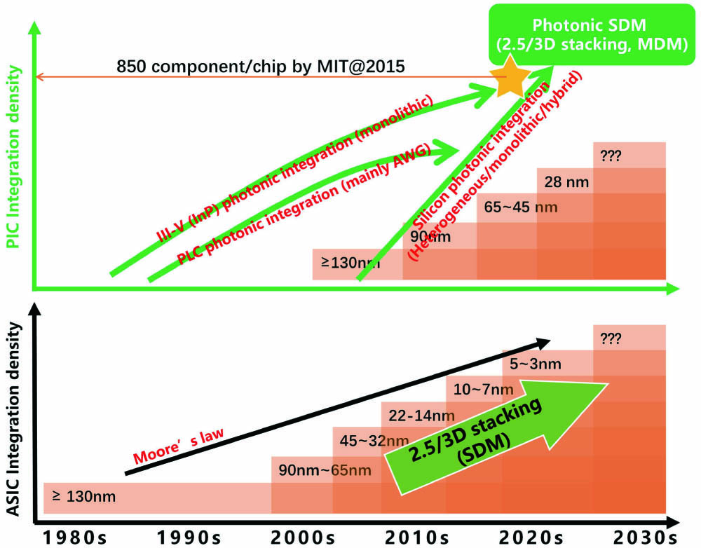

Set citation alerts for the article
Please enter your email address
© Copyright 2018-2021 | Chinese Laser Press. All Rights Reserved 沪ICP备15018463号-20