1Institute of Optoelectronics, Fudan University, Shanghai, China
2State Key Laboratory of Surface Physics, Key Laboratory of Micro and Nano-Photonic Structures of the Ministry of Education, and Department of Physics, Fudan University, Shanghai, China
3Centre for Quantum Physics, Key Laboratory of Advanced Optoelectronic Quantum Architecture and Measurement of the Ministry of Education, School of Physics, Beijing Institute of Technology, Beijing, China
4Beijing Key Laboratory of Nanophotonics & Ultrafine Optoelectronic Systems, School of Physics, Beijing Institute of Technology, Beijing, China
Low symmetry 2D materials with intrinsic in-plane anisotropic optical properties and high tunability provide a promising platform to explore and manipulate light–matter interactions. To date, dozens of in-plane anisotropic 2D materials with diverse band structures have been discovered. They exhibit rich optical properties, indicating great potential for novel applications in optics, photonics, and optoelectronics. In this paper, we thoroughly review the anisotropic optical properties and polaritons in many kinds of low symmetry 2D materials, aiming to elicit more research interest in this field. First, the optical properties of anisotropic 2D semiconductors, including interband absorption, photoluminescence, excitons, and band structure engineering for tuning optical responses, are introduced. Then fundamentals and advances in experiments of hyperbolic polaritons in anisotropic 2D materials, including phonon, plasmon, and exciton polaritons, are discussed. Finally, a perspective on promising research directions is given.
Since the discovery of graphene in 2004[1], amazing quantum phenomena of 2D materials have been unraveled, such as the distinctive half-integral quantum Hall effect[2,3], Hofstadter’s butterfly and fractal quantum Hall effect[4], and unconventional superconductivity in magic-angle graphene superlattices[5], which have made 2D materials fascinating ever since their birth. Furthermore, 2D materials exhibit strong light–matter interaction. For instance, single-layer graphene exhibits a considerable interband absorption of exactly in the infrared (IR) regime ( is the fine structure constant)[6,7]. More surprisingly, due to the quantum confinement and reduction in dielectric screening, robust excitonic absorption at room temperature can be as large as 20% in monolayer transition metal dichalcogenides (TMDCs)[8,9]. These make 2D materials a novel platform to explore light–matter interaction. Many unique optical properties in 2D materials have been revealed, including universal absorption regardless of the wavelength[7], helicity of valley excitons[10,11], near unity excitonic reflection and photoluminescence (PL) quantum yield[12,13], single-photon emission[14], Dirac-type plasmons[15], and so on. In addition, the high tunability of 2D materials dramatically enriches optical properties. In particular, due to the non-bonding nature of the van der Waals (vdWs) interlayer interaction, 2D materials can be arbitrarily stacked layer by layer to form homo/heterostructures without a lattice matching limitation[16,17], which in principle offers infinite freedom to manipulate optical properties. Well-known examples include intriguing interlayer excitons in heterostructures and moiré excitons in moiré superlattices[18–21].
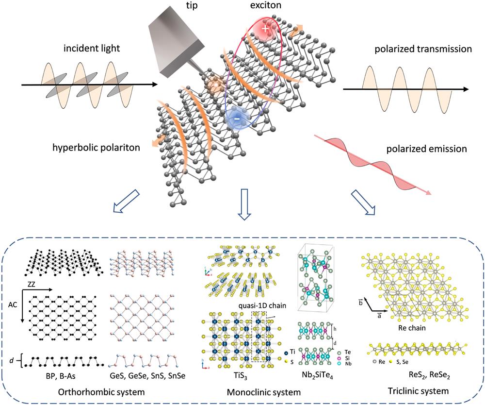
At present, hundreds of 2D materials with diverse band structures have been discovered experimentally, including metals, semimetals, semiconductors, insulators, magnetic materials, and superconductors[22–25]. Among them, a special type of 2D materials with in-plane anisotropic properties attracts abundant research interest due to the in-plane low crystal structure symmetry. The most representative and extensively studied one is black phosphorus (BP). BP joined the 2D family in 2014, when Li et al. at Fudan University first reported few-layer BP field effect transistors (FETs) with superior properties[26]. First, BP attracted attention due to its highly tunable properties and high carrier mobility, bridging graphene and TMDCs, such as a strongly thickness-dependent direct bandgap covering from the mid-IR (MIR) to the visible regime (0.3 to 2 eV from bulk to monolayer), and exactly complementing the bandgaps of graphene and TMDCs. Soon after, its anisotropic electrical, optical, mechanical, and thermal properties were discovered in both theory and experiment[27–30], which evokes (not only in BP) much attention to anisotropic 2D materials. As for optical properties, the anisotropy not only induces well-known phenomena such as linear dichroism in absorption and birefringence, but also renders additional freedom to control and detect light. On the other hand, anisotropy gives rise to different optical conductivities along different in-plane axes . In particular, when have different signs, the material can hold so-called hyperbolic polaritons (including phonon, plasmon, and exciton polaritons), whose iso-frequency contours (IFCs) are hyperbolas. These special polaritons with extremely large photonic densities of state (DOSs) and directional propagating rays are very fascinating in photonics[31]. Thus, anisotropic 2D materials benefit from the common merits of 2D materials, such as strong light–matter interaction and high tunability, and at the same time, with additional anisotropy, are expected to show much richer physics, which is very promising for basic research and practical applications in photonics and optoelectronics. In fact, optical anisotropy can be found in in-plane isotropic 2D materials with anisotropic nanostructures as well[15,32,33]. However, it should be noted there is an essential difference between low symmetry 2D materials and symmetric 2D materials with anisotropic nanostructures. The optical anisotropy in the former is due to the anisotropic band structure, which can be tuned by various electronic band structure engineering techniques. What is more, the working wavelength region can spread widely, ranging from terahertz (THz) to ultraviolet regions. The optical anisotropy of the latter is mainly due to the anisotropic effective dielectric constant in fabricated nanostructures, in which the tunability of optical properties and the working wavelength region are limited by the nanostructure fabrication.
To date, dozens of anisotropic 2D materials, including semiconductors and semimetals, have been discovered. According to the crystal structure, anisotropic 2D materials can be divided into orthorhombic systems [e.g., BP, black arsenic (B-As), group IV monochalcogenides MX (M = Ge,Sn; X = S, Se), etc.], monoclinic systems (e.g., 1T’ , ), and triclinic systems (e.g., , X = S, Se). With different crystal structures, anisotropic 2D materials exhibit diverse optical properties. For instance, in BP, strong interlayer interaction gives rise to multiple interband transitions with polarization along the armchair (AC) direction[34,35]; in group IV monochalcogenides, multi-valley band structure leads to multiple interband transitions as well but with different polarization dependences[36]; in , excitonic polarization dependence exhibits layer dependence though with a weak interlayer coupling[37,38]; in , anisotropic electronic structure gives rise to the prominent hyperbolic plasmon response[39]; in , hyperbolic phonon polaritons (PhPs) with high confinement and long lifetimes have been discovered[40]. In this paper, we thoroughly review the fundamental optical properties and polaritons of various anisotropic 2D materials, aiming to evoke more research interest in this field. The paper is organized as follows: after this introduction, we discuss the fundamental optical properties, including interband absorption, PL, exciton, non-linear optical properties, and band structure engineering in Section 2, where anisotropic materials are limited to semiconductors, including BP, group IV monochalcogenides MX (M = Ge, Sn; X = S, S), (X = S, Se), and . In Section 3, first, the hyperbolic polaritons including phonon, plasmon, exciton polaritons are introduced; then the engineering for hyperbolic polaritons and their applications are discussed. Finally, conclusions and perspectives for future research in this field are given in Section 4.
Sign up for Photonics Insights TOC. Get the latest issue of Photonics Insights delivered right to you!Sign up now
2 Optical Properties of Low Symmetry 2D Materials
2.1 Interband Absorption
Most optoelectronic devices work in the IR to ultraviolet regime, where the interband transition plays a critical role in light absorption. The interband transition is closely related to the material band structure, through Fermi’s golden rule: where () is the joint DOSs (JDOSs) involving both conduction () and valence () bands, is the transition matrix element, and is the Hamiltonian for light–matter interaction. In general, in the dipole approximation, can be expressed as , where is the dipole moment of the electron, and is the electrical field of light. defines the transition probability from band to band [41]. In anisotropic 2D materials, the band structure is anisotropic as well. Thus, the value of is polarization dependent, which results in anisotropic absorption. The band structure is layer dependent due to the interlayer interaction. Hence, we can gain insight into two main characteristics of anisotropic 2D materials from the absorption, namely, layer dependence and anisotropy. Next, we will particularly focus on these two characteristics of optical properties in anisotropic 2D materials.
2.1.1 Interband absorption in BP
BP belongs to the orthorhombic structure. As shown in Fig. 1, in-plane P atoms are covalently bonded, forming a hexagonal lattice with a puckered structure constituting two sublayers. According to atomic morphology, two main in-plane crystal axes are denoted as AC and zigzag (ZZ). During early studies of 2D BP, theoretical calculations predicted BP is always a direct bandgap semiconductor regardless of the thickness[27,42–44]. The bandgap shifts from Z point (bulk) to point (few or monolayer) in the Brillouin zone (BZ), with the energy ranging from 0.3 eV (bulk) to 2.0 eV (monolayer). Furthermore, theoretical studies also suggested the anisotropy in light absorption[27,43,44]. For example, the interband transition at point is allowed (forbidden) when incident light is polarized along AC (ZZ) direction. On the contrary, at point, it is forbidden (allowed) under AC (ZZ) polarization[43]. The polarization dependence of the interband transition can be understood by group theory or symmetry analysis[43,45]. Briefly, due to a mirror symmetry with respect to the plane, wave functions of the conduction band and valence band at point both have even symmetry with respect to the mirror plane. Consequently, when incident light is polarized along ZZ (-axis) direction, the transition matrix element is zero, giving rise to a forbidden transition. It should be noted, though, that selection rules will be relaxed with the interband transition away from the high symmetry point in BZ.
Figure 1.Light–matter interaction and atomic structures of anisotropic 2D semiconductors.
Experimentally, Xia et al. first measured the polarization resolved IR absorption of mechanically exfoliated BP film through a Fourier transform IR (FTIR) spectrometer[28]. Due to the relatively large thickness (), BP thin film showed a bulk-like absorption spectrum, where an absorption edge was observed at , corresponding to the bulk bandgap. The layer-dependent absorption property of atomically thin BP was not discovered until Li et al. performed an optical absorption study of one- to five-layer BP[34]. As shown in the reflection spectra of Fig. 2(a), a strong resonance peak, corresponding to the optical bandgap, was observed at 1.73 eV in monolayer BP. With increasing thickness, the optical bandgap redshifts to 1.15 eV in bilayer and 0.83 eV in tri-layer. In few-layer BP above the bandgap, additional absorption resonances were observed, such as peaks at and 1.93 eV in bi- and tri-layer, respectively. In fact, the multiple resonance absorption peaks originate from interband transitions between different valence sub-bands and conduction sub-bands at point as shown in Fig. 2(c). Due to the interlayer interaction, the original valence (conduction) band in monolayer splits into sub-bands in the Nth layer. Only interband transition from to (labeled as ,) with the same index is allowed; thus, -layer BP at point possesses interband resonances. Consistent with theory predictions, absorption measurements showed all of are strongly layer dependent, which redshifts with increasing layer numbers. Through the 1D tight-binding model, Li et al. gave a phenomenological description of the systematic evolution of with layer number and sub-band index , that is, , where is the monolayer bandgap, , and is the nearest neighbor coupling between adjacent layers for conduction (valence) band. Through fitting experimental data, and were obtained, with comparable to the theory prediction (), validating the model. It should be noted that, even without including an excitonic effect (as will be discussed in Section 2.3), the model can still well capture the evolution of the transition energy . In fact, this model is not only applicable to few-layer BP, but also to other 2D semiconductors, such as TMDCs. At the same time, Zhang et al. systematically studied IR absorption of the 2L–15L BP in MIR to near-IR (NIR) regime through FTIR, and multiple resonance absorption peaks were observed as well. Especially in thicker samples (e.g., 13-layer), at least four resonance absorption peaks were clearly discerned[35]. Zhang et al. revealed that the transition energy of can be well described by the quantum well based formula, suggesting that few-layer BP can be regarded as a natural vdWs quantum well, where sub-bands correspond to quantized bands in a quantum well due to quantum confinement. The anisotropy in absorption was revealed by absorption spectroscopy as well. As shown in Fig. 2(b), all exhibit the strongest absorption when light is polarized along AC. The relation between the absorption intensity and polarized angle (with respect to AC direction) follows the scaling .
Figure 2.Interband absorption of anisotropic 2D materials. (a) Absorption spectra of 1L, 2L BP (left)[34], bulk-like GeS (middle)[64], and 1L–3L (right)[37]. The photoreflectance of GeS is also shown in the middle panel. (b) Polarization dependence of interband absorption of BP (left)[35], GeS (middle)[64], and (right)[37]. 0° corresponds to AC direction for BP and GeS, but for , it corresponds to axis (Re chain). (c) Illustration of interband transitions at point of BP. (d) Photocurrent spectra of thin () (left)[99] and absorption spectra of thin () (right)[102]. (e) Layer-dependent bandgap and interband transitions. Left panel: first three transition energies of BP and versus layer number. Data are taken from Refs. [35,37,38]. Right panel: bandgap ranges of various anisotropic materials (BP, , MX, , NST) with thickness from bulk to monolayer. Data are taken from Refs. [35,37,38,60,97,102].
Although atomically thin BP possesses superb absorption properties, it is very unstable under ambient conditions[46–49]. Due to unpaired electrons on the surface, BP is reactive to , forming compounds on the BP surface. These compounds can be dissolved in air moisture and accelerate the degradation of BP. The degradation profoundly affects the BP optical properties. Wang et al. revealed that an optical bandgap of 3L has significant blueshifts even when exposed to air only within 5 min, accompanied by peak broadening and weakening[49]. In addition, the transition energy of with small and large is more sensitive to degradation, which can be well explained by the quantum well model. The instability is a bottleneck that hinders BP from practical applications. Nevertheless, there are some ways to protect BP from degradation, such as encapsulation with boron nitride (BN) layers[48,50,51], while there are still many limitations in practice.
With the same puckered crystal structure as that of BP (as shown in Fig. 1), B-As is regarded as a cousin of BP. B-As inherits superb properties of BP, such as strong in-plane anisotropy, large on–off current ratio, and highly tunable bandgap at the IR regime[52–55]. What is more, B-As has better ambient stability. Zhong et al. showed that few-layer B-As based FET still works even after exposure to air for one month[53]. Hence, B-As is a good candidate to complement BP. Unfortunately, to date, due to the limitation of synthesis of high quality B-As crystals, experimental study of optical properties of few-layer B-As is rather limited.
2.1.2 Interband absorption in group IV monochalcogenides
With orthorhombic structures, group IV monochalcogenides compounds MX (M = Ge, Sn and X = S, Se) have been extensively studied for their exceptional thermoelectric properties for decades. Now as a type of 2D vdWs material, they have regained extensive research interest[56–58]. Orthorhombic MX compounds exhibit a puckered layer structure similar to that of BP (see Fig. 1), and thus MX is regarded as the cousin of BP as well. Different from BP, monolayer MX lacks inversion symmetry, giving rise to additional unique properties, e.g., giant piezoelectricity[59], large spin–orbit splitting[60], multiferroics[61], and multi-valley band structure[36]. The ambient stability and environmental compatibility make 2D MX particularly attractive in applications as semiconductor devices. Using density functional theory (DFT) with the Heyd-Scuseria-Ernzerhof (HSE06) hybrid function, Gomes et al. predicted that the bandgaps of GeS (GeSe) and SnS (SnSe) enlarge from and in bulk to and 1.96 (1.33) eV in monolayers, respectively, covering the NIR to visible regime[60]. Almost all MX have indirect bandgaps, except for 1L SnSe and 1L–3L GeSe, while other studies showed multilayer GeS could have a direct bandgap as well[62]. In fact, theoretical calculations showed that the energy difference between direct and indirect bandgaps is tiny, comparable to room-temperature energy (). In view of this, MX can be regarded as quasi-direct bandgap semiconductors, which could be responsible for the discrepancies of the direct versus indirect nature among different studies. In addition, theoretical calculations also showed that in monolayer MX, conduction and valence band valleys always appear in pairs at almost the same k-point in BZ, one pair along the direction (AC) and the other along the direction (ZZ), giving rise to multiple interband transitions from different valleys with contrasted polarization dependence[36].
In experiments, due to the fragility of MX, atomically thin MX with high crystal quality is not available yet; nevertheless, anisotropic interband transitions have been demonstrated in their bulk-like thin films. Taking multilayer GeS as an example, through modulated optical spectroscopy (a powerful technique for probing the direct interband transition), two direct interband transitions ( and ) with a contrasted polarization dependence near the absorption edge were identified[62–64]. As shown in Fig. 2, the interband transition at is polarized along ZZ, whereas at is polarized along AC. Due to the different polarization dependence of and , the absorption edge () of multilayer GeS shifts from 1.6 to 1.65 eV when the light polarization changes from AC to ZZ direction. However, the origins of and stir controversy. Hsueh et al. assigned multilayer GeS to a direct bandgap semiconductor, and corresponds to the transition from the direct bandgap at point; is originated from the selection-rule forbidden transition near point along direction, evoked by the local structural symmetry breaking[62], while Totooczko et al. showed multilayer GeS has an indirect bandgap by comparing absorption and photoreflectance, which was rationalized by their DFT calculations[64]. According to their calculation results, and were assigned to transitions at point and point in ZZ direction, respectively. Similar to GeS, multiple interband transitions near the absorption edge with different polarization dependences of multilayer SnSe, SnS, and GeSe were revealed as well[65,66]. Multiple interband transitions are a consequence of the multivalley band structure in MX, which can offer a new platform for valleytronics.
2.1.3 Interband absorption in ReX2
Among anisotropic 2D materials, besides BP and its cousins, rhenium dichalcogenides (, where X = S, Se) attract abundant research interest as well[67–69]. is a member of TMDCs, with its atomic structure shown in Fig. 1. In each layer, Re atoms are sandwiched between two S atom sheets, and four Re atoms are grouped into parallelograms, forming a Re chain along the axis (ZZ). Different from hexagonal TMDCs (e.g. , ), belongs to the distorted 1T triclinic structure with a lower in-plane symmetry, which gives rise to anisotropic properties. is very air-stable. All of these make suitable for novel opto-electronic applications, although studies on 2D from different groups show discrepancies, particularly with respect to the direct or indirect bandgap nature and strongly coupled or decoupled interlayer interaction. Take as an example. Several theoretical calculations showed that from bulk and monolayer has a direct bandgap located at point of BZ[70–72]. However, other studies showed that the bulk bandgap is marginally indirect[73], or a bandgap with either direct or indirect nature depends on thickness[74,75]. As for interlayer coupling, PL peak positions and Raman phonons showed little and no layer dependence, indicating electronic and vibrational decoupling due to the weak interlayer interaction[70]. Consequently, bulk behaves like monolayer. However, contrary results were reported by ultralow frequency Raman spectroscopy[76–78], where force constants of interlayer shear modes were estimated as of those in [77], suggesting strong interlayer coupling. By using k-space photoemission microscopy, Gehlmann et al. found that electrons in the valence band are significantly delocalized across the vdWs gap in [73], also indicating considerable interlayer coupling. Similar controversies can be found in as well[38,72,79]. Studies have suggested that in , there coexist different stacking orders with different optical properties[77,78,80], which can interpret these contradictory results. To fully reconcile these discrepancies of , more studies are needed.
As for the absorption of , Ho el al. preliminarily performed a series of studies in bulk through modulated optical spectroscopy before joined the 2D family[81–84]. In bulk , two resonance peaks (labeled as and ) near the band edge were unambiguously discernable, and were assigned to direct interband transitions from the valence to the conduction band at different k-points. In , () centered at (1.52) eV occurs with incident light polarized parallel (vertical) to the axis. () in has the same polarization dependence but with a lower transition energy of (1.33) eV. Previous optical spectroscopy studies also showed that both bulk and have indirect bandgaps of and 1.19 eV, respectively, which are very close to direct bandgap values. The layer-dependent and anisotropic absorption properties of atomically thin (1L–7L) were first experimentally studied by Aslan et al.[37]. Three resonance peaks ( to ) were discerned, among which and correspond to those previously reported in the bulk counterpart, while at higher energy could be due to the onset of a band-edge free-carrier transition or an excited excitonic state of or . All three peaks exhibit obvious layer dependence, with , , and blueshifting from 1.47, 1.51, and 1.58 eV in bulk to 1.61,1.68, and 1.88 eV in monolayer, respectively. The blueshifts of , , and from bulk to monolayer in are much larger than those observed for the direct transitions [at point in BZ] in 2H-TMDCs (e.g., ) but smaller than those for indirect transitions (valence band extrema at point in BZ) in the same materials. In addition, Aslan et al. revealed a complex polarization dependence of and absorption in atomically thin . In monolayer, and exhibit a maximum for light polarized at and with respect to the axis, respectively, while in tri-layer, the maximum polarization angles change to and with respect to the axis, respectively, which are different from those reported in bulk by Ho et al. Similarly, in , two prominent absorption peaks near the band edge were observed as well. Through polarization-dependent extinction and PL spectroscopy in conjunction with DFT calculations, Arora et al. revealed that two prominent absorption peaks (labeled as and ) are actually superpositions of four different interband excitonic absorption peaks[38]. Due to the two-fold degenerated valence band maximum (VBM) and conduction band minimum (CBM) at point, four absorption peaks originate from the direct transition at point with different combinations of spin, with energy splitting from the exchange interaction. and also exhibit an obvious layer dependence, with transition energy blueshifting and 140 meV, respectively, when the thickness decreases from bulk to monolayer, comparable to those in . The polarization dependence of these four transitions is more complicated. In fact, there are controversies in the polarization dependence and interband transition assignment in [85], and the mechanism underlying the complex polarization dependence in atomically thin is still unclear. Further studies are necessary.
2.1.4 Interband absorption in other anisotropic 2D materials
New types of low symmetry 2D materials with different crystal structures have been discovered, though their bulk counterparts were already studied many years ago. For example, group IV–group V compounds (GeP, GeAs, SiP, SiAs) and group IV transition metal tri-chalcogenides (TMTCs) (, , , , , ), which belong to the monoclinic system, have been recently rediscovered as emerging anisotropic 2D materials[86–94]. Most of these materials are indirect bandgap semiconductors, except for . is a TMTC with a unique quasi-1D Ti-chain in layers (as shown in Fig. 1), which can be regarded as a quasi-1D material. Due to the much weaker interaction between quasi-1D chains, the exfoliated is usually needle shaped. Monolayer has been predicted in theory with a direct bandgap of and with a very high electron mobility up to ∼10,000 cm2/(V s)[95]. The photoresponsivity of devices based on shows a strong polarization dependence with the highest value reaching up to 2500 A/W[96]. All of these give great potential for a new generation of optoelectronic device applications as well. Unlike other 2D materials, theory calculation showed that the bandgap of is quite robust, exhibiting an direct bandgap at point for all thicknesses[97]. This is mainly attributed to the fact that the locations of CBM and VBM states are at the center atoms of , unaffected by interlayer coupling. Through theoretical calculations, Torun et al. suggested three interband transitions at point, among which the interband transition from the bandgap (with lowest transition energy) is allowed only when light is polarized along the out-of-plane direction, while the other two are both allowed when light is polarized along the in-plane axis (parallel to the Ti chain)[98]. Recently, through photocurrent spectroscopy, Lian et al. revealed anisotropic absorption with photon energy ranging from to in both thick () and thin () [as shown in Fig. 2(d)][99]. Both thick and thin exhibit resonance absorption peaks when light is polarized along the axis, in agreement with theoretical calculations. In thick , two absorption peaks and centered at 1.23 and 1.41 eV, respectively, were identified, while in thin , only centered at 1.34 eV was observed, indicating different band structures in thick and thin . According to their first-principles calculations, the CBM in thick shifts to Z point, giving rise to an indirect bandgap, and is due to the transition from the valence band to a higher conduction band at point; corresponds to two direct transitions near X and Z points. In thin , the band structure is similar to that of the monolayer, which has a direct bandgap at point due to the lack of Z point; corresponds to the direct transition at point, and is absent.
Although various anisotropic 2D materials have been discovered, those with a narrow bandgap located at MIR and far-IR (FIR) are really scarce, which could limit 2D materials for IR opto-electronics applications. Bulk layered and were reported with narrow bandgaps of and 0.3 eV in MIR, respectively[93,100], while the optical properties of their 2D counterparts are hardly known. Recently, (NST) was discovered as an IR anisotropic 2D material[101,102]. NST belongs to the monoclinic crystal system, possessing in-plane anisotropic atomic structure formed by a Te-(Nb, Si)-Te sandwich layer, which is similar to the 2H-TMDCs such as but with two types of atoms (Nb and Si) in the inner layer instead of one (Mo) in the (as shown in Fig. 1). Theoretical calculations suggest that NST has a narrow indirect bandgap ranging from 0.89 eV in the monolayer to 0.39 eV in the bulk, situating in the NIR to MIR regime[102]. Devices based on few-layer NST show a relatively high carrier mobility of and photon responsivity of 0.66 A/W. All of these suggest that NST is a good candidate for IR opto-electronic devices. Wang et al. studied the anisotropic absorption properties of atomic thin NST through FTIR spectrometry[102]. As shown in Fig. 2(d), a series of polarization-dependent absorption resonances [labeled as A, and C] centered at , 0.66, and 1.1 eV was observed. Among them, A and B are allowed when light is polarized along the axis, whereas and C are allowed when light is polarized along the axis. In addition, the absorption linear dichroism in NST is switchable through changing the wavelength, that is, NST absorbs more light polarized along the axis in photon energy ranging from 0.49 to 0.66 eV, whereas it absorbs more light polarized along the axis when above 0.66 eV. Through first-principle calculations and group theory, these interband transitions can be well assigned as transitions from the first valence band to different conduction bands [e.g., for A (B) and for ] at different k-points in BZ.
2.2 Photoluminescence
PL is the re-emission of light from material after absorbing a photon of higher energy, which is another fundamental optical process in materials. Materials with high quantum yield (ratio of the radiative photon number and generated electron–hole pairs) PL have great advantages for luminescent device applications such as lasers and light emitting diodes (LEDs). PL results from the radiative recombination of electrons in the conduction band and holes in the valence band, termed as interband PL. The selection rules of interband PL and interband absorption are consistent since they are governed by the same transition matrix elements. Different from absorption, the PL process is prone to emit photons with the lowest energy, and thus the recombination of electrons and holes usually occurs at the bandgap. Even when carriers (electron or hole) are excited at a higher energy level, they will soon relax back to the CBM (or VBM) before recombination, as shown in Fig. 3(b). If there are defect states located within the bandgap, PL due to defect states emitting longer wavelengths could be prominent, especially under low temperatures. It should be noted that interband absorption is insensitive to defect states due to the low density of defect states compared to that at band extrema. Hence, it will give rise to the difference between PL and absorption peak positions, which is termed as a Stokes shift. The Stokes shift can be a gauge for crystal quality. Due to defect states, PL is not a good method to determine the intrinsic bandgap; nevertheless, it offers vitally important emission properties of the material.
Figure 3.Photoluminescence spectra of anisotropic 2D materials. (a) PL of BP. Left two panels: PL of monolayer[34] and multi-layer (thickness from 4.5 to 46 nm) at 77 K[116]. Middle right panel: PL peak positions in atomically thin BP reported by several groups[34,49,103–110]. Right panel: linear polarization dependence of PL emission in monolayer BP[34]. Emission intensity follows function, where is the angle with respect to AC direction. (b) Illustration of PL process. (c) PL of multilayer GeS ()[63]. Top panel: polarization dependent PL spectra of GeS, where “A” (“∥a”) corresponds to excitation (detection) polarized along AC direction. Bottom panel: PL emission intensity versus detection polarization angle. (d) PL of [85]. Top panel: PL spectra with different detection polarization angles of few-layer () at 4 K (one at 300 K shown in inset). At low temperature, five PL peaks can be discerned. Bottom panel: first two PL peak intensities versus detection polarization angle, where 0° corresponds to axis (Re chain). (e) PL of [123]. Top panel: PL spectra under different detection polarization angles of multi-layer () at low temperature (20 K). Spectra are divided into two regions, where D denotes defect states PL, and X denotes intrinsic interband PL. Bottom panel: emission intensities of D and X versus detection polarization angle , where axis is parallel to the quasi-1D Ti-chain.
As a direct bandgap semiconductor, BP is expected to have a strong PL signal. In early studies of BP, several groups observed pronounced PL in atomically thin BP but with huge discrepancies in PL peak positions[34,49,103–111]. For example, PL in monolayer BP was reported by several groups with emission energy ranging from 1.3 to 2 eV, and ranging from 1.1 to 1.6 eV in bilayer and 0.8 to 1.0 eV in tri-layer [as shown in Fig. 3(a)]. Such huge discrepancies in PL peak positions are most likely due to the vastly different sample quality, since BP degrades under ambient conditions and gives rise to a blueshift of PL peak position. On the other hand, degradation also introduces defect states, rendering PL emission at a lower energy[49]. To suppress degradation, Li et al. encapsulated BP by BN, and observed PL at , 1.1, and 0.8 eV in monolayer, bilayer, and tri-layer respectively, with a small Stokes shift of , attributed to defect states[34]. Recently, Yan’s group reported PL at 1.69, 0.98, and 0.86 eV in ultrahigh quality 1L–3L BP (no Stokes shifts)[49,110], respectively.
Since PL is sensitive to defect states, one can manipulate PL properties through defect engineering. Defect state PL with emission energy lower than the bandgap can widen the working wavelength range of devices. In addition, it has been demonstrated as a good candidate for single-photon emitters as well. Pei et al. reported a bright defect state PL in monolayer BP at through artificially introducing oxygen defects by controllable etching with plasma[107]. By using a plasma-enhanced chemical vapor deposition (PECVD) oxide substrate, Xu et al. obtained defect state PL centered at energy of as well, whose intensity was 33.6 times stronger than the intrinsic one[112]. This defect state PL was further confirmed by the sublinear relation between emission intensity and excitation intensity in a power dependence study. PL due to defect states was also observed in few-layer and bulk BP[113–115].
Only thin BP, with a layer number less than five, was investigated in early PL studies, with PL situated in the visible to NIR range, readily detectable by a grating spectrometer. Chen et al. investigated MIR PL emission in thicker BP () by FTIR spectroscopy[116]. They showed that PL emission in multilayer BP is quite bright, comparable to InAs multiple quantum well samples grown by molecular beam epitaxy (MBE). PL peak positions in the IR regime can also be well fitted through the 1D tight-binding model (as applied to absorption peaks) with consistent fitting parameters, further confirming the direct bandgap nature in multilayer BP. Inspired by superb PL properties in BP, anisotropic MIR LEDs and lasers based on BP were achieved in experiments as well[117,118], suggesting the great potential of BP for IR luminescent device applications.
As mentioned above, the polarization dependence of interband PL and absorption is consistent. As shown in Fig. 3(a), the PL emission of BP is linearly polarized along AC, with intensity following a scaling[34]. Interestingly, defect state PL has the same polarization dependence as well[112]. PL intensity also exhibits excitation polarization dependence. When the excitation light (wavelength of 532 nm) is polarized along AC, PL intensity is maximal, which is mainly due to the anisotropic absorption of the excitation light[106].
2.2.2 PL in group IV monochalcogenides
As quasi-direct bandgap semiconductors, group IV monochalcogenides MX (M = Ge, Sn and X = S, Se) are expected to have prominent PL under room temperature in the NIR to visible range. Take GeS as an example. Ho et al. reported bright PL centered at in multilayer GeS () at room temperature [as shown in Fig. 3(c)][63]. PL is due to the recombination of interband transition . It should be noted that there are two interband transitions near the band edge, namely, and , but only one PL peak assigned to is discernable. This is because the excited holes from transition at a lower energy level will soon relax to VBM before radiative recombination. A similar situation can be found in few-layer BP, where only one PL peak with the lowest energy can be observed among multiple interband transitions. Surprisingly, Zhao et al. showed that laser thinned monolayer GeSe exhibits eight PL peaks ranging from the visible to IR range[119], and the intensities and positions of these PL peaks are abnormally independent of temperature, since in general, PL intensity can be significantly enhanced under low temperatures due to the suppressed nonradiative recombination. These results need further experimental verification. Due to the atomic structure similar to BP, the polarization dependence of PL in MX is consistent with that in BP. For instance, GeS PL emission is linearly polarized along AC direction. When the excitation light (e.g., wavelength of 633 nm) is polarized along the AC direction, the maximal PL intensity can be achieved due to anisotropic absorption [as shown in Fig. 3(c)].
2.2.3 PL in ReX2
Under room temperature, two prominent PL peaks with different polarization dependences in can be observed[37,38], which are consistent with those observed in the absorption spectrum. Due to controversial findings of the band structure, studies related to PL in also exhibit discrepancies. For example, in , Tongay et al. first reported that PL peak position slightly blueshifts from to when the thickness decreases from bulk to monolayer[70]. PL intensity decreases with the decrease in sample thickness, indicating no indirect-to-direct bandgap transition similar to that in . Calculations by Tongay et al. suggested that is always a direct bandgap semiconductor regardless of thickness. Aslan et al. later reported that the lowest energy PL peak position in exhibits a larger blueshift when thickness is reduced from bulk (PL at 1.40 eV) to monolayer (PL at 1.65 eV), and through a comparison between PL and absorption spectra, they assigned PL at 1.40 eV in bulk to the indirect bandgap emission, slightly below the direct bandgap at 1.47 eV[37]. Mohamed et al. quantitatively obtained a low PL quantum yield of in 1L–7L regardless of the layer number, which is at least one-order of magnitude smaller than those in monolayer 2H-TMDCs (e.g. ) with direct bandgaps[120]. These low PL quantum yields were ascribed to the indirect bandgap nature in . Similarly, in , Zhao et al. reported that the PL position slightly shifts from 1.26 eV in bulk to 1.32 eV in monolayer, and the PL intensity decreases monotonically when decreasing the layer number, suggesting a much weaker interlayer interaction and no indirect bandgap to direct bandgap transition[121]. Ho et al. also evaluated PL quantum yields of , comparable to that of [85]. In addition, discrepancies can be found in the PL line shape as well. For example, Aslan et al. showed that in atomically thin , PL intensity due to transition is stronger than that due to ( at a higher energy than ), indicating the possible presence of a lower lying indirect transition or of rapid nonradiative relaxation associated with defects[37]. In other reports, PL intensity due to is obviously stronger than that due to [85,120]. The discrepancies in PL studies might be due to different crystal qualities or stacking orders of .
Under low temperature, the fine structure of PL in can be clearly distinguished. As shown in Fig. 3(d), Ho et al. found three additional PL peaks centered at 1.63 (1.45), 1.64 (1.47), and 1.65 (1.48) eV (labeled as , , and respectively) in the few-layer () at 4 K, which were assigned to interband excitonic PL at different k-points in BZ with higher energy[85]. Among them, the polarization of () was consistent with that of (). In addition, Jadczak et al. observed two series of four PL peaks centered between 1.63 and 1.67 eV in bulk at 7 K[122]. One series of four PL emission peaks was polarized along the axis, while the other series was perpendicular. These two series of PL are ascribed to excited states of excitons and (discussed in the next section).
2.2.4 PL in other anisotropic 2D materials
Linearly polarized PL has also been studied in other anisotropic 2D materials. As a quasi-1D direct bandgap semiconductor, is expected to have a strong anisotropic PL. Recently, Curto et al. reported an NIR PL centered at 0.91 eV in multilayer (thickness )[123], as shown in Fig. 3(e). PL emission in is partially linearly polarized with maximal (minimal) intensity along the axis, parallel (perpendicular) to the quasi-1D chain, with a polarization anisotropy ratio of at room temperature and increasing to at 20 K. Due to anisotropic absorption, PL in also exhibits excitation polarization dependence (laser wavelength ). At low temperatures, defect state PL with lower emission photon energy is prominent. Interestingly, such PL exhibits a contrary polarization dependence compared to that of interband PL, whose maximal emission intensity is along the axis, as shown in Fig. 3(e).
Although a cousin of , has an indirect bandgap, due to the in-plane quasi-1D chain atomic structure, it is expected to exhibit strong PL as well. Pant et al. reported polarized PL centered at 1.45 and 1.8 eV in thin film. PL at 1.8 eV is due to the indirect bandgap, whose polarization dependence mainly results from the geometry anisotropy of the quasi-1D chain structure[124]. For the width of the quasi-1D chain much smaller than the excitation light wavelength, absorption will be stronger when the excitation light is polarized along the chain. However, the PL anisotropy ratio is only to 10.8, smaller than that in true 1D nanowires or carbon nanotubes. The discrepancy might be attributed to the large effective permittivity or interactions between quasi-1D chains.
2.3 Excitons
Above, the absorption and PL were discussed without considering Coulomb interactions between electrons and holes. In fact, due to the enhanced quantum confinement and reduced dielectric screening, Coulomb interactions in 2D materials between electrons and holes are prominent even at room temperature, giving rise to electron–hole bound states termed as excitons. In 2D materials, excitons play a dominating role in optical properties, significantly enhancing light–matter interaction. For example, without excitons involved, the absorption of monolayer graphene is only 2.3%[7], while in monolayer TMDCs at exciton resonance, the absorption can be as large as [8,9]. There are many excellent reviews of excitons in 2D materials[125–127]. Here we mainly focus on excitons in low symmetry 2D materials. Before a detailed discussion on representative materials, basic properties of excitons will be briefly reviewed.
As mentioned above, an exciton is formed by a pair of electrons and holes due to Coulomb interactions, which can be simply conceived as an analogy to a hydrogen atom. Analogous to hydrogenic states, there is a series of excitonic states as illustrated in Fig. 4(a), which can be labeled by principal and magnetic quantum numbers as (, ), where and . With the same notation as in the hydrogen atom, can be denoted as states. Due to selection rules determined by the symmetry of the exciton wave function, in general, only s states can be observed in a single-photon absorption process. As shown in Fig. 4(a), the resonance energy at the exciton ground state (1s), typically called optical bandgap, is lower than the true bandgap (quasiparticle bandgap) , with the energy difference termed as exciton binding energy . The binding energy is a critical parameter of the exciton, which measures the energy needed to separate the bounded electron–hole pairs, and gauges the strength of Coulomb interactions. In bulk semiconductors, due to the strong screening from the material itself, the binding energy is usually comparable to or smaller than room-temperature energy (); thus, the exciton can be observed only at low temperatures, while in atomically thin 2D materials, screening from the material is reduced significantly. In addition, quantum confinement restricts electrons and holes in-plane, and hence, the binding energy can acquire a surprisingly large value, e.g., in monolayer TMDCs[126]. Interestingly, in anisotropic 2D materials, anisotropic effective mass makes carriers more mobile along one crystal axis than the other (see Table 1). It is plausible to anticipate excitons with quasi-1D properties, such as larger binding energy.
Figure 4.Excitons in anisotropic 2D materials. (a) Schematic illustration of excitons. Top panel: illustration of the optical absorption of an ideal 2D semiconductor[126]. Series of exciton states (, , , etc.) below the quasiparticle bandgap are shown. Bottom panel: real-space illustration of excitons in an anisotropic 2D material (left) and a typical exciton wave function calculated for monolayer BP (right)[44]. (b) Layer-dependent excitons in few-layer BP. Top left panel: typical extinction spectrum of BP (tri-layer) with high crystal quality on PDMS substrate[141]. state can be clearly discerned as indicated by the red arrow. Top right panel: layer dependence of and transition energies and the quasiparticle bandgap in 2L–6L BP[141]. Bottom left panel: layer dependence of absorption due to excitons in 2L–7L BP, where is the universal absorption of monolayer graphene[129]. Bottom right panel: absorption near the corresponding band edge due to the continuum part of each interband transition in 2L–7L BP[129]. The continuum absorption is nearly independent of the material thickness. (c) Calculated optical absorption with/without excitonic effect in monolayer GeS (left) and GeSe (right)[36]. X corresponds to AC direction. (d) Excitonic absorption in . Left panel: transmission and calculated absorption spectra of monolayer and bulk [38]. Near band edge, two prominent peaks can be discerned, which are superpositions of four excitonic resonances labeled as . Right panel: differential reflectance spectra of multi-layer () under different polarized incident lights (with respect to the axis, as shown in inset)[144]. Four excitonic absorption peaks labeled as can be discerned. (e) Excitons in other anisotropic 2D system. Top left panel: schematic illustration of band structure, exciton A, and sideband A′ in bulk . Top right panel: experimental PL spectrum and calculated absorption spectrum of with/without exciton–phonon interactions[146]. Bottom left panel: illustration of exciton–phonon coupling via phonon mode modulated ligand field transition in . Bottom right panel: linear dichroism spectrum of a thin bulk flake at 5 K[147].
Tran et al. first theoretically studied the anisotropic exciton in 1L–3L BP[44]. They predicted that suspended monolayer BP has a large binding energy of , and what is more interesting, they found that the wave functions of typical bright excitons (e.g., ) are anisotropic, specifically, more extended along the AC direction to form striped patterns, similar to those found in nanowires [as shown in Fig. 4(a)]. They ascribed this quasi-1D like exciton wave function to the anisotropic mobility of electrons. Subsequently, Gomez et al. predicted that the binding energy of monolayer BP on a substrate would be significantly reduced to only 380 meV, suggesting a strong screening effect from the substrate[104]. Later on, comparable binding energies of freestanding and supported BP were predicted in theory through different calculation methods[43,137,138].
In experiments, through PL excitation (PLE) spectroscopy, Wang et al. first obtained the exciton binding energy of a surprisingly large value, , in monolayer BP on a substrate[106]. They observed that a PL signal centered at (corresponding to the optical bandgap) was resonantly enhanced with excitation energy at 2.45 eV, which was attributed to the resonance absorption of the quasiparticle bandgap edge extracted as . This unusually large binding energy of supported monolayer BP was attributed to the quasi-1D excitonic feature by Wang et al. Nevertheless, as mentioned above, there are huge discrepancies in the monolayer BP PL peak position, which could give rise to different binding energies. For example, later studies by Yang et al. reported two PL peaks in monolayer BP on a substrate with central wavelengths at (1.76 eV) and (1.6 eV)[108]. The former was assigned to ground state exciton () PL, and with a comparison to the measured quasiparticle bandgap of by Pan et al. using scanning tunneling spectroscopy (STS)[139], Yang et al. determined the binding energy in supported monolayer of only , much smaller than that reported by Wang et al. but comparable to previous theoretical predictions. It should be noted that PL at was assigned to the trion (charged exciton), leading to a large trion binding energy of , almost five times higher than that in the isotropic TMDC monolayer (e.g. ), which was rationalized by their quasi-1D charge complex model. However, such a claim was challenged by later theoretical studies[138,140]. Calculation results by Chaves et al. showed that, although larger than the usual trion binding energy in TMDCs, even the trion binding energy in suspended monolayer BP is only , and decreases to in supported BP, which is much smaller than the claim by Yang et al.[138]. Due to the discrepancy, the validity of the 1D model of the trion binding energy in monolayer BP was questioned by Chaves et al.
Very recently, through reflection spectroscopy, Wang et al. reported excited exciton states ( and ) in high quality monolayer BP on a polydimethylsiloxane (PDMS) substrate[110]. Through extracting energy differences between , () and , () from the spectrum, binding energy of in monolayer BP on PDMS was obtained, slightly larger than previous predictions. On the other hand, since states are expected to be more Rydberg-like (as discussed later) with an increasing exciton quantum number , and states can be assumed to follow the ideal 2D hydrogenic model. Then the binding energy can be simply estimated as , consistent with previous predictions. In addition, it should be noted that the optical bandgap reported by Wang et al. was , and by comparing to the measured quasiparticle bandgap of by STS, it suggests a comparable binding energy of in supported monolayer BP. All of these results indicate that, regardless of the quasi-1D excitonic feature in BP, the binding energy in supported monolayer BP is roughly , rather than , as claimed by Wang et al.[106]
Due to the direct bandgap nature of BP, regardless of thickness, the layer dependence of excitons can be studied in experiment. Through absorption spectroscopy, Zhang et al. observed the states in few-layer BP (2L–6L) with high crystal quality on PMDS substrates at room temperature [as shown in Fig. 4(b)][141]. The energy difference between and states was directly extracted from the spectra as 122, 87, 76, 62, and 58 meV for 2L to 6L BP, which decreases with increasing thickness. As for 2s states in thicker BP (>6L), the energy separation of the state is too close to discern. In the 2D hydrogenic model, it is well known that the energy separation of and states accounts for 8/9 of total binding energy. Through numerical calculations, Zhang et al. showed that the binding energies of 2L–6L BP on PDMS are 213, 167, 139, 120, and 106 meV, respectively, suggesting that the energy separation between 1s and 2s states accounts for only about half of the total binding energy. This is mainly due to the nonlocal dielectric screening of Coulomb interactions in 2D materials. In fact, this nonlocal screening induced deviation between excitonic Rydberg series and 2D hydrogenic Rydberg series was earlier studied in monolayer TMDCs[128]. Therein, Olsen et al. proposed a generalized hydrogen model for nonlocal screened excitons in 2D materials, where the media dielectric constant ɛ in the expression in the hydrogen model was substituted by an effective 2D dielectric constant through averaging the screening over the extent of the exciton[130]. Remarkably, in this generalized hydrogen model, the binding energy can be generally simplified as , where is the 2D sheet polarizability of the 2D material, suggesting that is independent of the excitonic effective mass and depends only on . On this basis, Zhang et al. further proposed an effective polarizability as , where and account for the screening from the substrate and -layer BP itself, respectively. can be expressed as [141]. The model can well fit the layer-dependent in few-layer BP, with reasonable fitting values of and , comparable to previous theorical calculations, which suggests that the model is feasible. In addition, this model predicts that of suspended monolayer BP and that supported on PDMS are 762 and 316 meV, respectively, in good agreement with previous theoretical predictions.
Besides the binding energy, Zhang et al. further investigated the layer-dependent absorption strength of excitons in 2-7 L BP on a PDMS substrate[129]. In common sense, thicker materials induce stronger absorption strength. Surprisingly, for exciton absorption in 2D BP, less is more. Zhang et al. found that frequency-integrated exciton absorption was enhanced in thinner BP [as shown in Fig. 4(b)]. This interesting phenomenon can be quantitatively explained by the quantum well model, i.e., the integrated excitonic absorption is mainly determined by , where is the thickness of the sample (layer number for BP), and is the modular square of the excitonic wave function at the origin with a scaling law. This gives rise to a relation for the excitonic absorption strength, hence, the thinner the sample, the larger the excitonic absorption. After taking into account the substrate screening effect, this relation was modified as . Equally interestingly, Zhang et al. found that absorption from the continuum transition close to the band edge is a constant , where is the fine structure constant with a value of 1/137 ( is the universal absorption constant in graphene), and is the reduced effective mass in the AC (ZZ) direction. This universal continuum absorption in BP is due to the cancellation mechanism between the transition matrix element and 2D JDOS, i.e., the band-parameter-dependent terms are perfectly canceled out. It should be noted that in -layer graphene, pairs of sub-bands are involved in the optical absorption, giving rise to -fold absorption compared to the single layer. On the contrary, due to the bandgap at point in BZ, only one pair of sub-bands in BP is involved for continuum absorption near the bandgap; hence, the continuum absorption near the bandgap is constant regardless of thickness.
2.3.2 Excitons in group-IV monochalcogenides
As for group-IV monochalcogenide compounds MX, there are pairs of excitons from different valleys with different polarization dependences due to the multi-valley band structure. Xu et al. systematically investigated the exciton in monolayer MX in theory, as shown in Fig. 4(c)[36]. The lowest energy exciton A is polarized along AC direction in all MX, with binding energies of 0.98, 0.38, 0.5, and 0.28 eV in GeS, GeSe, SnS, and SnSe, respectively, in good agreement with earlier calculation results[131,142,143]. Binding energies of the lowest energy exciton B in ZZ direction were calculated as 0.77, 0.36, 0.5, and 0.28 eV in GeS, GeSe, SnS, and SnSe, respectively. In the MX bulk counterpart, the binding energy is relatively small, less than 0.1 eV. The substrate screening effect also significantly affects the exciton binding energy, e.g., A exciton binding energy in monolayer GeSe significantly shrinks from 0.38 eV in a suspended one to 0.19 eV in one supported on a substrate. It should be noted that among four monolayer MX, exciton in GeS is the most localized due to the largest binding energy, while exciton in SnSe is the most delocalized. Binding energy is closely related to the screening length of the material itself but weakly depends on the reduced mass. The exciton spatial distribution anisotropy in GeX is larger than that in SnX. The radii of A exciton in GeS along AC and ZZ are 6.74 and 4.46 Å, respectively, while in SnS, the A exciton radius is 15 Å along both directions.
2.3.3 Excitons in ReX2
Zhong et al. first studied excitons in freestanding monolayer in theory. Based on their results, the lowest-energy exciton in at point with a binding energy of 1.07 eV exhibits a perfect 8-shaped polarization dependence, while that of with binding energy of exhibits only partial polarization dependence, due to the mixture of two bright excitons at and points with different polarization dependences[132]. Theoretical calculations by Echeverry et al. suggested that in both monolayer and , due to the doubly degenerated VBMs and CBMs at point, the lowest energy exciton with different spin combinations splits into four due to the exchange interaction, with average binding energies of 0.74 and 0.57 eV in and , respectively[72].
In experiments, Arora et al. reported four excitonic absorption and PL peaks with different spin combinations at point in [as shown in Fig. 4(d)[38]], discussed in Section 2.1. Dhara et al. reported four excitonic absorption peaks near the bandgap in few-layer under low temperatures [Fig. 4(d)][144]. Different from those of , two prominent peaks were assigned as bright exciton absorption at Z and points in BZ according to previous DFT results[133], and two additional weaker peaks were ascribed to the splitting of singlet and triplet states of excitons. Dhara et al. also revealed that the existence of low lying dark excitons causes an anomalous PL intensity variation at 30 K in a temperature dependence study, which was rationalized by the rate equation model. In addition, through low temperature PL spectroscopy, Jadczak et al. revealed that resonance , as reported by Aslan et al. in bulk , is composed of several excited excitonic states of ground state excitons and [122]. Through a 3D hydrogenic Rydberg model, the binding energies of excitons and were estimated as and 0.08 eV, respectively. It should be noted that the binding energy in bulk is much larger than that in other bulk materials, which could be attributed to the weak interlayer coupling in , resulting in the exciton being confined in individual layers. The binding energy of monolayer supported on graphene was directly determined as 0.52 eV by Qiu et al. through measuring the quasiparticle bandgap by STS and the optical bandgap by reflectance spectroscopy, which could also be continuously tuned from 0.46 to 0.68 eV by electrostatic gating[134]. In addition, through gate-dependent low temperature PL spectroscopy, Wang et al. reported negative trions in few-layer (1L–5L) [135]. The trion binding energy is strongly layer dependent, and can be as large as 60 meV in monolayer, almost two times larger than that in isotropic TMDC monolayers.
2.3.4 Excitons in other anisotropic 2D materials
With quasi-1D structure, is expected to have robust excitons with large binding energy. Theoretical studies showed that in monolayer , there are three interband transitions at point, accompanied by three bright excitons with binding energies of 0.59, 0.68, and 0.32 eV, respectively[98]. The lowest energy exciton located at is bright only for out-of-plane polarization, but with a quasi-1D nature, theoretical calculations for suggested that the wave function of an exciton in is almost isotropic[145]. In addition, in spite of the robust nature of a quasiparticle bandgap with little layer dependence, Lian et al. found that binding energy exhibits strong layer dependence, which is significantly enhanced from in bulk to in monolayer[99]. The large binding energy in monolayer results in the lowest energy excitonic absorption () at . This value is inconsistent with the aforementioned , and needs further study to resolve the discrepancy. In experiments, by using STS and photoelectrochemical measurements, Mendoza et al. obtained a quasiparticle bandgap and optical bandgap in thin film () of and 1.07 eV, respectively[136]. The binding energy was determined as , in agreement with the predicted result of 0.1 eV by their calculations.
Very recently, through PL and reflectance spectroscopy, Zhou et al. reported an unconventional exciton with hybrid dimensionality in 2D , where the electrons constituting the excitons are confined within 1D phosphorus–phosphorus chains, while the holes are extended over the 2D plane[146]. This unique exciton with binding energy of (in with ) can strongly couple with phonons, resulting in a broad sideband PL at the low energy side of the prominent PL [as shown in Fig. 4(e)]. The exciton–phonon coupling induced energy shift of the sideband PL was , in good agreement with their calculation results. Both exciton emission and an emergent sideband feature show linear dichroism, and due to the electron–phonon coupling, both dramatically redshift with increasing temperature, in contrast to the slight change of the quasiparticle bandgap. This unique hybrid low dimensional system is very promising for enriching excitonic physics and further understanding exciton–phonon coupling.
The recent emergence of 2D vdWs magnets provides a new platform to study excitonic physics with intrinsic magnetic order. Hwangbo et al. reported the observation of excitons coupled to ZZ antiferromagnetic order in layered antiferromagnetic semiconductor , as manifested by the near-unity linear polarization of exciton PL and absorption under low temperatures and almost vanishing above the Neel temperature[147]. In addition, the strongly coupled exciton–phonon bound states can be observed even in atomically thin samples (e.g., 3L–5L) below the Neel temperature, and more surprisingly, over states on the high energy side of exciton resonance were clearly resolved as shown in Fig. 4(e), which were ascribed to the strong modulation of the ligand-to-metal charge-transfer energy by electron–lattice interactions. Klein et al. reported an extremely anisotropic electronic band structure of layered A-type antiferromagnetic semiconductor CrSBr, in which the anisotropic ratio of electron effective mass can be as large as [148]. Such a strong quasi-1D electronic character gives rise to strongly anisotropic excitons with large binding energies of 0.88 and 0.9 eV for the two lowest energy excitons in the monolayer limit, and strong exciton–phonon coupling as revealed by resonances of the 1s state exciton at detuning energy () corresponding to and phonons in the PLE spectrum. In this quasi-1D electronic system combined with magnetic order, the magneto-exciton physics calls for further exploration.
2.4 Nonlinear Optical Properties
The above discussions are all in the realm of linear optics, where the polarizability of the material depends linearly on the electric field of light. This is valid only when incident light intensity is low. With a high intensity of incident light, depends nonlinearly on , that is, where is the vacuum permittivity, and is the th-order susceptibility. is the normal linear susceptibility, responsible for linear absorption, reflectance, and transmittance; is responsible for second-order nonlinear effects, such as second-harmonic generation (SHG), optical rectification, and Pockels effect; is responsible for third-order nonlinear effects, such as third-harmonic generation (THG), saturation absorption, two-photon absorption (TPA), and optical Kerr effect. It should be noted that second- or even-order nonlinear effects exist only in non-centrosymmetric materials, while third- or odd-order nonlinear effects can take place in all materials. Due to the quantum confinement effect and anisotropy for anisotropic 2D materials, nonlinear optical properties are unique. Recent studies have been performed to investigate nonlinear optical effects in anisotropic 2D materials, and optoelectronic devices based on nonlinear optical effects, such as anisotropic saturable absorbers, ultrafast pulse generation, optical switches, and optical diodes in anisotropic 2D materials, have been demonstrated. There are dedicated review papers for nonlinear optical properties and applications in anisotropic 2D materials[149,150]. In this section, nonlinear optical properties including saturable absorption, harmonic generation (SHG and THG) of low symmetry 2D materials will be briefly discussed.
2.4.1 Saturable absorption
Saturable absorption is a phenomenon in which absorption of light decreases with increasing incident light intensity, which results from the Pauli-blocking principle. Under strong incident power, CBM and VBM are filled with excited electrons and holes, respectively, impeding the interband transition and giving rise to a reduction in absorption [as shown in Fig. 5(a)]. The saturable absorption effect is very useful for ultrafast pulsed lasers, optical modulators, and so on; thus, it is an important research field in nonlinear optics and has been extensively studied. The saturable absorption coefficient can be expressed as where and are the saturable and non-saturable absorption coefficients, respectively, and and are incident light intensity and saturable intensity, respectively. Based on the Beer–Lambert law, the saturable absorption induced transmittance can be expressed as where is modulation depth. In experiments, through open (or closed) aperture Z-scan and I-scan methods, the normalized transmittance spectrum can be obtained.
Figure 5.Nonlinear optics of anisotropic 2D materials. (a) Saturable absorption. Left panel: schematic illustration of saturable absorption. Middle left panel: power-dependent transmittance with incident polarization angle changing from axis (AC) to axis (ZZ) in the exfoliated thick BP flake (thickness )[155]. Middle right panel: typical open aperture Z-scan curves of SnSe nanosheet dispersion under 230 fs excitation pulses with wavelength of 1030 nm[160]. Right panel: polarization-dependent absorption of (thickness ) at low incident power of and at high power of (left top), and polarization-dependent ratio of absorption between that under 1.55 and incident power (left bottom)[156]. The right one is a schematic of excited-state absorption in . (b) Third harmonic generation (THG). Left panel: schematic illustration of THG. Middle panel: typical THG spectrum of multilayer BP flake (thickness ) under excitation wavelength of (left), and polar plot of polarization dependence of THG from BP flake (thickness ) on glass substrate (right), where red and purple arrows indicate AC and ZZ directions, respectively[163]. Right panel: THG power of BP in transmission (orange) and in reflection (blue) versus thickness. The resonance THG occurred at thickness as indicated by pink area[161]. (c) Second harmonic generation (SHG). Left panel: schematic illustration of SHG. Middle left panel: SHG spectra from bilayer and monolayer pumped by a laser at 1558 nm. Insets are polar plots of SHG parallel components from bilayer and monolayer [165]. Middle right panel: SHG intensity in 1L–8 L [165]. Right panel: SHG of SnS film (thickness ) at different excitation wavelengths[166].
The saturable absorption in anisotropic 2D materials was first studied in few-layer BP dispersions obtained by liquid phase exfoliation with a broad bandwidth ranging from visible (400 nm) to MIR (at least 1930 nm)[151–153]. The saturable absorption response in BP dispersions is much stronger than that in graphene dispersions. Afterwards, Li et al. revealed the salient layer dependence of saturable absorption in BP flakes[154]. The saturable absorption induced transmittance increase in thicker exfoliated BP flakes (1100 nm) was around eight times larger than that in thinner BP (25 nm). Such thickness dependence is useful for pulse generation since nonlinear saturable absorbers with different parameters are needed.
Saturable absorption also exhibits polarization dependence. Sotor et al. found that BP flakes (thickness ) exhibit saturable absorption but with different modulation depths when light (wavelength of 1560 nm) is polarized along AC and ZZ directions. The highest transmittance is obtained under ZZ polarization, consistent with linear absorption polarization dependence[155]. With a further increase in light intensity, a roll-off effect (reverse saturable absorption) in the transmittance spectrum with ZZ polarization was observed, ascribed to the TPA effect, whereas it retains saturable absorption with AC polarization [as shown in Fig. 5(a)]. Anisotropic saturable absorption was also reported in bulk by Liu et al., which can be transformed to reverse saturable absorption by rotating incidental light polarization[156]. For instance, the normalized absorption increases under a polarized angle of 0° (with respect to the axis) due to saturable absorption, while it decreases under an polarized angle due to reverse saturable absorption [as shown in Fig. 5(a)]. Since reverse saturable absorption occurs at relatively low intensity power, and due to the lack of free carriers in undoped , the finding was ascribed to excited state absorption, consistent with angle-resolved photoemission spectroscopy (ARPES) results[157]. The same group found that nonlinear optical absorption depends on the stacking order. Saturable absorption occurs only in AB stacking at polarized angles from 30° to 105° (with respect to the axis), and is absent in AA stacking. The reverse saturable absorption due to excited state absorption occurs in both stackings, but with a larger anisotropy in AB stacking[158]. This peculiar polarization and stacking order dependence were attributed to an additional absorption channel of exciton–exciton annihilation in AB stacking.
In fact, the saturable absorption effect is closely related to linear absorption. According to Fermi’s golden rule, linear absorption at different wavelengths with different transition matrix elements (polarization dependent) and JDOSs, changes the final excited states differently, giving rise to different saturable absorption effects. Zhang et al. investigated saturable absorption effects in SnSe flakes (thickness ) at dual wavelengths of 800 and 850 nm[159]. The anisotropic ratio of the modulation depth between AC and ZZ directions was 6.7 at 800 nm wavelength, much larger than that of 1.4 at 850 nm. In addition, the saturable absorption coefficient and modulation depth at 800 nm were found to be smaller than those at 850 nm, indicating weaker saturable absorption. On this basis, novel all-optical switching with a higher on–off ratio of was proposed. Ye et al. studied the saturable absorption effect at a wavelength of 1030 nm in few-layer SnSe dispersion[160]. Since incident photon energy is lower than the bandgap of few-layer SnSe (average thickness of ), the saturable absorption effect was attributed to the depletion of defect states located in the bandgap. With increasing incident light intensity, reverse saturable absorption due to TPA was observed. The transition from saturable absorption to reverse saturable absorption in thicker SnSe (average thickness of ) dispersion was observed as well but with higher incident power, which is related to the layer-dependent bandgap in SnSe.
2.4.2 Second- and third-harmonic generation
Harmonic generation is a process converting incident photons at frequency into a higher frequency photon as shown in Figs. 5(b) and 5(c), which can be employed to produce a broadband wavelength-tunable coherent light source. SHG () and THG () are most frequently used for frequency conversion applications; hence, here we mainly focus on SHG and THG processes in anisotropic 2D materials.
As a centrosymmetric material, BP permits only THG. THG in BP has been studied by several groups[161–163]. A typical THG signal is shown in Fig. 5(b), with the peak centered at , exactly three times the frequency of the pump light (wavelength 1560 nm)[163]. As anticipated, THG is polarization dependent, and the intensity of THG in BP can be expressed as where is the intensity of the pump light, is the third-order susceptibility tensor of BP, subscripts and refer to AC and ZZ directions, respectively, and is the polarized angle of pump light with respect to the AC axis. Different from the two-fold polarization dependence of linear absorption, THG exhibits a four-fold polarization dependence pattern, which is mainly due to the nonzero component. It should be noted that maximal THG intensity is obtained not along the AC direction as shown in Fig. 5(b). In fact, due to the higher tensor ranks of and , the polarization dependence of SHG or THG could be very different from linear absorption. Even in isotropic material, SHG or THG could be anisotropic. Hence, they are usually used to determine the crystal orientation of materials.
The intensity of THG in BP also exhibits strong layer dependence. Rodrigues et al. found that THG in atomically thin BP can be significantly enhanced due to excitonic resonance [as shown in Fig. 5(b)][161]. With the pump light wavelength at 1560 nm, which is close to the excitonic resonance absorption of 3L BP, the effective third-order susceptibility in 3L BP can be enlarged to times that in graphene. In a non-resonance regime, THG also has layer dependence in BP with thickness ranging from 5 to 50 nm. The maximal THG signal was obtained in BP with to 20 nm thickness, which was attributed to the competition between different absorptions of pump light and THG in materials. THG has also been studied in other anisotropic 2D materials. In particular, monolayer exhibits strong and anisotropic THG, in which the third-order susceptibility is of , almost one order of magnitude larger than that in 2H TMDCs such as [164].
SHG exists only in non-centrosymmetric materials, such as 2H-TMDCs with odd-layer thickness. Interestingly, Song et al. found that anisotropic SHG in atomically thin exhibits an opposite dependence on thickness[165]. Strong SHG exists only in even-layer , whereas it is negligible in odd-layer [as shown in Fig. 5(c)]. This unusual layer-dependent SHG is due to the unique distorted 1T structure of , i.e., inversion symmetry exists in mono (odd-) layer but breaks in bi- (even-) layer. In group IV monochalcogenides MX, prominent and anisotropic SHG was observed as well [see Fig. 5(c)][166]. Theoretical studies predicted that effective second-order susceptibility in monolayer MX can be as large as 10 nm/V within a broadband regime (photon energy from 0.8 to 4 eV)[167], which is remarkably high among those reported in other 2D materials, such as 0.16 nm/V in and 0.001 nm/V in BN. The large anisotropy of SHG in monolayer MX could be also closely related to the intrinsic ferroelastic and ferroelectric orders[168].
2.5 Tuning Optical Properties Through Band Structure Engineering
2D materials composed of single or several atomic layers, are very sensitive to external perturbations, such as the dielectric environment, electrical field, and strain. Thus, the band structure can be easily modulated artificially, that is, band structure engineering. Band structure engineering has been extensively studied in 2D materials, through various tuning methods, including electrical gating, applying strain or high pressure, chemical doping or intercalation, alloying, stacking vdWs homo or heterostructures, and so on[169]. Due to band structure engineering, novel properties beyond natural properties of materials have been revealed; one of the most famous examples is the unconventional superconducting in magic angle twisted bilayer graphene. Thus, band structure engineering is vitally important, not only for fully exploring the novel properties of materials in fundamental research, but also offering more possibilities for device design and optimization in practical applications. Anisotropic 2D materials with polarization dependence can offer additional freedom for band structure engineering. In this section, several types of band structure engineering to manipulate optical properties of anisotropic 2D materials will be discussed, particularly for BP, since band structure engineering of BP has been most extensively studied, and serves as a good representative.
2.5.1 Electrical field effect
In practice, applying an electrical field is the most feasible way to achieve tunable optoelectronic devices. When 2D materials are under a vertical (along out-of-plane direction) electrical field, the band structure distorts in real space with the wave functions of electrons and holes moving to opposite directions and partially tunneling into a forbidden bandgap, giving rise to a redshift of interband absorption, termed the Franz–Keldysh effect. Due to the strong quantum confinement effect in 2D materials, it is also called the quantum-confined Franz–Keldysh effect. As mentioned above, excitons usually dominate the optical properties in 2D materials. Exciton resonance energy redshifts with an external electrical field, which is also known as the quantum-confined Stark effect. In addition, since atomically thin materials can be approximated as natural infinite quantum wells, interband transitions are allowed only between valence and conduction sub-bands with the same quantum number (e.g., in BP). In the presence of a vertical electrical field, the additional otherwise selection-rule forbidden interband transitions (e.g., , ) could occur due to broken inversion symmetry. In experiments, the vertical electrical field is usually applied through the gate voltage based on FETs. Gate voltage not only supplies a vertical electrical field, but also changes the carrier populations (doping effect), which can blueshift the interband transition energy due to Pauli-blocking. In such a case, the interband transition energy shift will be nonlinear due to the competition between the electrical field effect and doping effect. Theoretical and experimental studies have shown that interband absorption peaks in few-layer BP redshift first at a low gate voltage and then blueshift at a higher gate voltage due to the quantum-confined Franz–Keldysh or Stark effect and Pauli-blocking, respectively[170–172]. Hybrid transitions such as and were observed as well. In fact, the electrical field and doping effect in FET can be separated by applying a dual gate voltage. By stacking heterostructures, materials can float in a vertical electrical field to avoid the doping effect. Through BN encapsulated BP devices with BN serving as the dielectric layer, Chen et al. revealed the pure electrical field effect on PL emission of few-layer BP (), as shown in Fig. 6(a)[173]. With a moderate displacement field up to 0.48 V/nm, PL emission with linear polarization can be continuously tuned from 3.7 to 7.7 μm, and it is expected to redshift to longer than 7.7 μm with a further increased field, which suggests the widely tunable IR light emission in BP. However, under the electrical field, PL intensity is reduced due to the spatial separation of electron and hole wave functions. Through in situ surface doping of potassium (K) on few-layer BP, where the carrier distribution is different between top and bottom BP surfaces, Kim et al. introduced a vertical electrical field in BP flakes[174]. Due to the giant Stark effect, the semiconducting BP was converted into a semimetal as a consequence of the bandgap closing, which was monitored by ARPES. What is more interesting, at the critical semiconductor to semimetal transition point, BP becomes an anisotropic Dirac semimetal, in which the electronic band disperses linearly (quadratically) along AC (ZZ) direction. In addition, under an ambient condition, the unintentional doping induced electrical field effect on few-layer BP was observed, as manifested by the redshift of the optical bandgap and appearance of hybrid transitions, which was further confirmed by the intentional chemical doping through vapor[35].
Figure 6.Band structure engineering of anisotropic 2D materials. (a) Electrical field effect on BP. Top left panel: schematic illustration of the BN-sandwiched device with graphene as top gate and Si substrate as bottom gate for applying vertical electrical field[173]. Top right panel: PL spectra of the 20-layer BP under different displacement fields () ranging from 0 to 0.48 V/nm[173]. Middle left panel: bandgap of the 20-layer BP extracted from PL spectra (dots) and first-principles calculations (curve) versus [173]. Bottom left panel: schematic illustration (top) and ARPES spectra (bottom) of BP band structure under different surface K-dopings[174]. Bottom right panel: absorption spectrum of a 9L BP before and after chemical doping through vapor (top) and enlarged view of the hybrid peaks between and (bottom)[35]. (b) Strain and pressure effect. Left panel: schematic illustration of application of uniaxial strain (top)[177], biaxial strain (middle)[181], and pressure (bottom)[188]. Right top panel: normalized PL spectra of multilayer BP () under zero strain, compressive strain ( along the zigzag direction), and tensile strain ( along the zigzag direction)[177]. Right middle panel: linear shift rates of interband transition (, , and ) peaks induced by biaxial strain versus layer number in 2L–10L BP[181]. Dots are experimental data, and solid curves are fittings through the tight-binding model. Right bottom panel: relative change of the optical bandgap of BP versus pressure[188]. Dots are experimental data, and solid curves are the fittings. (c) Alloying and intercalation. Top panel: crystal structure of [195] (left) and absorption spectra of with different constituent ratios x from 0 to 0.83 (right)[190]. Middle panel: schematic illustration of intercalation process by CTAB to form the BP superlattice (left) and high resolution TEM images of BP before and after intercalation (right)[195]. After intercalation, in-plane lattice parameter negligibly changes but interlayer distance has nearly two-fold enlargement. Bottom panel: electrochemical gate current as a function of the applied electrochemical potential (left), and PL signal observed at different stages of intercalation (right)[195]. (d) Homo and heterostructures based on BP. Top panel: schematic illustration of the crystal structure and band diagram of few-layer BP and monolayer heterostructure (left), and PL spectra of different thickness BP and heterostructures at 80 K[200]. Bottom panel: illustration of BN encapsulated 1L and 2L twisted BP homostructure and TEM image of a 5.7° twisted 1L/2L BP structure (left), scale bar 2 nm. PL spectra of the 1L, 2L BP and 19° twisted BP homostructure (right)[203]. An emerging moiré optical transition at 0.83 eV is observed in twisted homostructure.
Strain and pressure affect band structure in the same way in essence, i.e., modification of the lattice constants to tune the band structure, which can be easily understood in the tight-binding model. For example, the monolayer BP bandgap can be approximately expressed as , where and are hopping parameters between different atoms[175]. In general, the modulus of hopping parameter is proportional to , where is the distance between atoms connected by hopping parameter . Changes in lattice constants induce changes in hopping parameters, hence the bandgap. It should be noted that hoping parameter can be a positive or negative value, e.g., in monolayer BP and . The sign of determines the blueshift or redshift of the bandgap with increasing (or decreasing) lattice constants.
In-plane uniaxial strain can be applied by bending or stretching the substrate, or by introducing wrinkles in the material [as shown in Fig. 6(b)][176,177]. Experimental studies have shown that uniaxial strain can efficiently tune the bandgap size. For example, in few-layer BP with moderate uniaxial strain, Kim et al. reported that PL wavelength can change from 5.5 μm (0.66% compressive strain) to 3.2 μm (1.21% tensile strain), corresponding to the bandgap change from 0.22 to 0.53 eV [see Fig. 6(b)][177]. For anisotropic 2D materials, it is natural to anticipate that a uniaxial strain effect on band structure will be different when strain is applied along different directions[178,179], while experimental studies found that changes in bandgap and resonance absorption peaks above the bandgap are almost the same with strain along AC and ZZ directions[35,180]. This counterintuitive result was ascribed to different Poisson ratios along AC and ZZ directions. Previous studies showed that the Poisson ratio along AC direction is positive, which means that the puckered height of monolayer BP will decrease (increase) under the tensile (compressive) strain along AC. On the contrary, the Poisson ratio along ZZ direction is negative, which means that the puckered height changes in the opposite way[29]. The different changes in monolayer puckered height cancel the difference between the strain effect along AC and ZZ directions. Recently, Wang et al. reported that the strain effect for interband absorption in few-layer exhibits strong orientation dependence[102], in particular, for transitions B and , which blueshift (redshift) with tensile strain along the axis ( axis). Other interband absorption peaks exhibit anisotropic strain effects as well, manifested by the different shift rates of the absorption peak with strain along different axes.
In-plane biaxial strain can be commonly applied through the thermal expansion of the substrate underneath the 2D material, whose thermal expansion coefficient should be much larger than that of the 2D material [as shown in Fig. 6(b)][176,181]. Different from uniaxial strain, the biaxial strain effect is isotropic and believed to tune the band structure more efficiently. In addition, Huang et al. revealed that in-plane biaxial strain can efficiently modulate the interlayer coupling in few-layer BP, as manifested by the strongly layer-dependent strain effect[181]. According to their results, 1% in-plane biaxial compressive (tensile) strain can induce increase (decrease) in interlayer coupling, which is remarkable. More surprisingly, they found that the biaxial compressive strain in few-layer BP strengthens interlayer coupling, which is abnormal since the interlayer distance is anticipated to increase with in-plane compressive strain due to the Poisson effect. This unusual result is actually due to the unique puckered atomic structure of BP. More specifically, under biaxial compressive strain, the interlayer distance increases, but the “effective distance” determining interlayer coupling decreases, resulting in the enhancement of interlayer coupling.
To tune the interlayer interaction, applying pressure is the most direct method. Generally, hydrostatic pressure up to several to dozens of GPa can be applied through a diamond anvil cell (DAC) [as shown in Fig. 6(b)][182,183]. Under such high pressure, the material properties will undergo prominent changes, such as bandgap closing and crystal structure phase transition. For atomically thin 2D materials supported on a substrate, due to the adhesiveness between the material and the substrate, it is prone to induce non-hydrostatic pressure. In fact, if the substrate is stiff enough, the 2D materials undergo uniaxial strain along the out-of-plane direction[184,185]. Pressure can directly reduce the interlayer distance and increase interlayer coupling, which can shrink the bandgap size. For example, under 1.8 GPa, the bandgap of bulk BP is closed[186,187]. Recently, Huang et al. revealed that the pressure effect on band structure of BP exhibits strong layer dependence, e.g., under 1.8 GPa, the bandgap of bilayer BP does not shrink but enlarges[188]. This layer-dependent pressure effect results from the competition between the strengthened interlayer coupling and enlarged bandgap of the monolayer (the puckered height in monolayer decreases, inducing a larger bandgap). Their results show that a moderate pressure () induces relative change in interlayer coupling.
2.5.3 Alloying and intercalation
Alloying is a very traditional strategy to tune the band structure. Due to the weak interlayer coupling in , the bandgap is hardly tuned by thickness, while it can be efficiently tuned by alloying. In alloys, the optical bandgap can be continuously tuned from 1.62 (1.52) to 1.31 (1.26) eV in monolayer (bulk) by changing the constituent ratio x from zero to one[189]. In B-As–phosphorus alloys (), which keeps the orthorhombic structure with a puckered honeycomb lattice like that of BP or b-As but with two elements [as shown in Fig. 6(c)], the bandgap can be continuously tuned from 0.3 to 0.15 eV by changing the constituent ratio x from 0 to 0.83[190,191]. At the same time, the anisotropy is always retained. This gives great potential for long-wavelength optoelectronic applications.
Besides alloying, due to their interlayer non-bonding nature, layered 2D materials possess a physical vdWs gap, where guest species can be intercalated[192]. Usually, due to the small atomic size, the alkali ion is chosen as the guest species for intercalation, which can significantly change the carrier density and even induce a crystal structure transition, hence affecting the material properties. Studies showed that interaction is orientation dependent for anisotropic materials, e.g., intercalated ions have a more favorable channel along ZZ direction in BP[193,194]. While due to the high reactivity of an alkali ion, the intercalated materials are unstable under an ambient condition. In addition to alkali ions, a stable organic molecule [such as cetyl-trimethylammonium bromide (CTAB)] can also be chosen for intercalation. Due to the large size of the molecule, the intercalation can significantly increase the interlayer distance, giving rise to weakened interlayer coupling. Taking BP as a model system, Wang et al. intercalated CTAB into bulk BP through the electrochemical method, as shown in Fig. 6(c)[195]. Their atomic force microscope (AFM) and X-ray diffraction (XRD) results suggested that the interlayer distance increases more than 115% after intercalation, effectively isolating the single layer to form a monolayer superlattice. Through leveraging the electrochemical current, bilayer, tri-layer, or few-layer (even four to 10) BP superlattices can be engineered as well. PL was observed in mono-, bi-, and tri-layer superlattices at energies of 2.26, 1.75, and 1.38 eV, respectively. These PL energies are slightly higher than those of intrinsic BP, due to the strain induced bandgap expansion or orbital symmetry breaking caused by intercalation. Since monolayer BP can be obtained only by mechanical exfoliation with low yield and small lateral size at present, organic molecular intercalation offers an avenue to overcome these bottlenecks. The intercalated monolayer BP superlattice is very stable under ambient conditions. Thus, this technique is vitally important for 2D BP in both research and applications. More broadly, intercalation is a promising engineering technique, since intercalating different functional species into layered 2D materials could achieve a versatile material platform for both studies and applications.
2.5.4 Van der Waals homo/heterostructures
Due to the non-bonding vdWs interlayer interaction, 2D materials can be stacked arbitrarily with the same or different materials to form homo- or heterostructures without a lattice matching requirement. Based on the band alignment, heterostructures are divided into three types. In type I, both VBM and CBM of one material are located inside the bandgap of the other material; in type II, VBM and CBM of two stacking materials are staggered; and in type III, the CBM of one material is lower than the VBM of the other material. Due to the staggered band alignment in type II heterostructures, the excited electrons and holes can separately reside in different materials and form interlayer excitons. With the merits of a long lifetime and strong Stark effect, interlayer excitons have been extensively studied in type II heterostructures based on isotropic TMDCs[196]. It is expected that anisotropic materials could bring in anisotropy for interlayer excitons. Unfortunately, as far as we know, there is no experimental study on interlayer excitons in anisotropic heterostructures yet, even though a few studies revealed a superb anisotropic photo-response based on BP heterostructures[197–199]. In addition, in type I heterostructures, excited electrons and holes can transfer from material with a wider bandgap to another material, giving rise to an increase in light emission intensity. Recently, Zong et al. revealed that few-layer BP and monolayer form a type I heterostructure [as shown in Fig. 6(d)][200]. Due to the larger bandgap in monolayer , photo-excited electrons and holes are transferred from to BP, giving rise to enhancement in MIR PL intensity at a wavelength of 2.79 μm [PL of 4 nm (8L) BP]. Although the enhancement of PL decreases with increasing thickness of BP, this enhancement effect can persist up to the wavelength of 3.89 μm. It should be noted that in their heterostructure, BP and were stacked with random interlayer angles. The aligned stacking angle could affect PL efficiency, which deserves further study.
The twisting interlayer angle also dramatically enriches the phase diagram of homo/heterostructures. In particular, with a moiré superlattice, new properties emerge, such as unconventional superconductivity in magic angle twisted graphene, moiré excitons, and strongly correlated states in TMDC moiré superlattices[127,201,202]. In homo/heterostructures based on anisotropic materials, due to the lower symmetry, interlayer twisting is expected to be unique. For example, in homo/heterostructures based on graphene or TMDCs with hexagonal structure, the prominent moiré effect can be observed only within a tiny interlayer twisted angle (). Recently, Zhao et al. revealed that a strong moiré effect persists even at a large angle of in mono- and bilayer BP homostructures, as manifested by a new PL emission peak at a lower photon energy with polarization different from PL in mono- and bilayer BP [as shown in Fig. 6(d)][203]. Their DFT calculation suggested that such strong moiré effects in BP are not only related to the rectangular lattice of phosphorene but also due to the bandgap at point. Cao et al. theoretically investigated the 90° twisted bilayer BP earlier[204]. They showed that interlayer hybridization still exists for the conduction band but is absent for the valence band, and as a consequence, the transport and optical anisotropy can be switched by gate voltage. Subsequently, Srivastava et al. experimentally demonstrated resonance tunneling diodes based on 90° twisted BP homostructure[205]. At present, the study of homo/heterostructure involving BP is still in its infancy, and calls for more systematic studies in the future.
3 Polaritons of Anisotropic 2D Materials
3.1 Fundamentals and Probe of Polaritons
3.1.1 Fundamentals of polaritons
The concept of polaritons was first proposed by Kun Huang in 1951, describing the hybrid modes of a radiation field and lattice vibration in ionic crystals[206]. The solutions reveal two dispersive branches—the so-called PhPs. “Polariton” was further coined by Hopfield in 1958 based on the implication of polarization and photons, when applied to the interaction of incident light with excitons, namely, exciton polaritons[207]. In principle, polaritons are quasiparticles that contain both photons and collective oscillations of polarization charges (electric dipoles) under the illumination of light. Such electric dipoles can originate from the collective oscillation of free carriers due to the Drude response, or phonons in polar crystals and excitons in semiconductors, forming so-called plasmon polaritons, PhPs, and exciton polaritons, respectively. Note that these electric dipoles provide the negative real part of permittivity (positive imaginary part of conductivity), which is key for sustaining polaritons at the interface between dielectrics and the host material.
When the thickness of the host material is much smaller than the polariton wavelength, only the in-plane optical response is prominent. Such polaritons in thin films of layered 2D materials have gained much attention since the discovery of plasmon polaritons in graphene[15,208,209], and promise high field confinement and good tunability. The dispersion of polaritons in such a thin film limit is intrinsically determined by the sheet optical conductivity of the film itself: where and are the frequency and in-plane wave vector of polaritons, respectively, is the vacuum permittivity, is the dielectric constant of the surrounding environment, and is the sheet optical conductivity, which follows , with the optical conductivity of the bulk and the film thickness.
For 2D materials with in-plane anisotropy, the sheet optical conductivity takes the complex tensor form , written as , where , represent the principal components of the tensor (these components are dispersive with frequency , and we omit them for simplicity). Note that in this review, we mainly consider the tensor with zero nondiagonal elements. Assume that the material is lossless, so that there are only imaginary parts of conductivities with and , and the wavelength of the plasmon is much smaller than that of light. The dispersion relation of surface waves can be simplified as[210]where , is the vacuum wave vector, and are in-plane wave vector components of polaritons. By fixing the frequency , the in-plane IFC can be plotted in momentum space, which governs the optical dynamics of polariton propagation. For example, in isotropic surfaces such as graphene, where all the time, Eq. (6) indicates that the geometry of the contour is a circle, and the polariton wavefront propagates isotropically. In anisotropic surfaces where and , , the contour is quasi-elliptic with the long axis along the direction of the smaller conductivity component, which implies that the same wave vector of polaritons along different crystal axes will lead to splitting of the resonance frequency. However, at the frequency regime where the conductivities along the two principal axes have opposite signs, that is, , the IFC appears as a hyperbola [as shown in Fig. 7(a)]. This topological transition of the IFC resembles the Lifshitz transition, where the deformation of the Fermi surface from a closed to an open geometry significantly affects the electronic properties[211].
Figure 7.Schematic of polariton topological transitions. (a) IFCs in the momentum space and the component of the electric field in real space of surface plasmons supported by BP in purely anisotropic, quasi-circular, and hyperbolic regimes[231]. (b), (c), (d) Hyperbolic regimes induced by anisotropic phonons, plasmons, and excitons for phonon[232], plasmon[39], and exciton polaritons[110], respectively.
Polaritons with hyperbolic contours () are well known as hyperbolic polaritons, exhibiting great advantages compared to those in isotropic materials. For example, the open geometry of the contour in momentum space leads to theoretically infinite wave vectors and consequently extremely high DOSs. It should be noted that the wavefront and energy flow direction in anisotropic surfaces are not necessarily the same. It is the group velocity that dictates the energy propagation, which is also orthogonal to the IFC. The asymptotes of the hyperbolic curve are expressed as , and the perpendicular direction, namely, the direction of the polariton beam, is always along . In other words, a polariton propagates directionally on the hyperbolic surface. This peculiarity can be used to realize abnormal manipulation of polariton beams, such as focusing, negative refraction, and reflection[212–218]. In extreme cases, the asymptotes are parallel to one of the coordinate axes, while the energy flow is then parallel to the other, giving rise to highly ray-like polaritons, which is also known as the canalization effect[219,220].
The hyperbolic characteristic in layered material is attributed to the sign-changing conductivity along different crystal axes (). To be more precise, one of the axes is conductive (inductive) while the other is dielectric (capacitive), the mechanisms of which are diverse for different types of polaritons. Take plasmon polaritons as an example. The electromagnetic response of the material originates from free carrier intraband transitions and bound carrier interband transitions, which can be described by the Drude–Lorentz model: where the index , is the Drude weight, and denote the spectral weight and frequency of the interband resonance, respectively, and and represent the full width at half maximum (FWHM) of intraband and interband transitions, respectively. The first term on the right-hand side of Eq. (7) describes the Drude response of free carriers, which leads to a positive imaginary part of the conductivity, and the second term accounts for the interband transition, which provides a negative imaginary part of conductivity below the resonance frequency. The interplay between them could result in a critical point where . Apparently, in anisotropic 2D materials, the effective mass, spectral weight, and frequency of interband transitions can be different along two principal axes, leading to splitting of the critical points and formation of the hyperbolic regime as in Fig. 7(c), which can be further manipulated by strain, intercalation, chemical or electrostatic doping, and so on.
Now let us discuss PhPs in polar dielectric crystals. A high reflectance is observed in the reststrahlung band (RB), which is between the transverse optical (TO) and longitudinal optical (LO) phonon frequencies. It is analogous to the high reflectance below the plasma frequency in plasmonic systems, such as metals. The coherent lattice vibrations (phonons) in polar crystals play a role similar to free carriers in metals to sustain polaritons. The difference is that phonons are bound states. The optical conductivity induced by phonon resonance can be expressed by the Lorentz model as well, with as the resonance frequency, which serves as the critical point. As a result, the anisotropic phonons along two crystal axes generate a hyperbolic regime as shown in Fig. 7(b). Such hyperbolic PhPs intrinsically possess ultra-long lifetimes (narrow scattering width) and high figures of merit compared to plasmon polaritons, due to the damping only from the scattering of optical phonons[40]. On the other band, the hyperbolic characteristic is intrinsically fixed because of the stubborn phonon frequency, though it has been successfully tuned extrinsically by twisted stacking[221–227] and substrate engineering[228,229].
As for exciton polaritons in 2D semiconductors, excitons as bound states are also depicted by the Lorentz model, which enables at a certain frequency regime. As a result, they are able to sustain propagating exciton polaritons. In particular, in anisotropic 2D materials such as BP, exciton absorption is prohibited when incident light is polarized along the ZZ direction but allowed in the AC direction, leading to a dielectric response in ZZ direction with . Then, the hyperbolic characteristic can emerge at the region where , as shown in Fig. 7(d). The exciton polariton is actually a bosonic quasiparticle constituted of an exciton and a photon, which is promising for high temperature Bose–Einstein condensation (BEC) due to the exceedingly light effective mass[230].
In fact, in-plane hyperbolic dispersion from visible to microwave frequency ranges has already been realized in artificial metasurfaces. However, metasurfaces demand complicated design and fabrication of sophisticated subwavelength structures, which could hinder more extensive applications. More importantly, due to the energy dissipation and limitations on the fabricated geometric size of structure elements, the wave vector of the hyperbolic polariton in metasurfaces cannot be large. Therefore, natural hyperbolic 2D materials, with merits of natural atomic scale size and high tunability, provide a promising platform for hyperbolic polaritons.
3.1.2 Probe of polaritons
Unlike other optical measurements (e.g., absorption, PL), direct illumination of light from free space on materials is unable to excite polaritons due to the momentum mismatch of photons and polaritons. Some methods have been explored to compensate for the momentum mismatch, including both near- and far-field techniques.
Far-field techniques usually detect the reflection, transmission, absorption, or scattering of a specimen at macroscopic distance with the aid of spectrometers. To excite polaritons, incident light can couple to a prism to obtain an extra momentum as ( is the refractive index of the prism, and is the angle of incidence). Thus, a prism with a high refractive index is needed, either in touch with (Kretschmann configurations) or above (Otto configurations) the surface, as shown in Fig. 8(a). On the other hand, a periodic grating array fabricated by the side of the material can also provide additional momentum to excite polaritons, with the momentum expressed as ( is the grating period, and is an integer). The above methods are to probe propagating polaritons. Localized non-propagating resonant modes of polaritons in artificial nanostructures (e.g., cavities, particles, disks, and ribbons) can be directly probed by incident light, such as the localized surface plasmon resonance (LSPR) of graphene nanoribbons shown in Fig. 8(b). Far-field techniques with merits of convenience, multifunctionality, and full-wave detection are powerful tools to investigate polaritons in momentum space.
Figure 8.Methods to probe polaritons. (a) Schematic to stimulate polaritons in the far field. Due to the momentum mismatch, light in free space is unable to excite polaritons directly. Additional momentum can be supplied by Kretschmann or Otto configuration, fabricating gratings by the side of material or resonant nanostructures[238]. (b) Resonant modes of LSPR in graphene nanoribbons with different widths[15]. [(c)-a] Schematic illustration of the near-field technique to image propagating plasmon polaritons at the surface of graphene on with s-SNOM. [(c)-b, c, d, e] Near-field amplitudes of interference pattern close to graphene edges (blue dashed lines), defects (green dashed lines and dot), and at the boundary between single and bilayer graphene (white dashed line)[208]. (d) Diagram of STEM-EELS experimental setup. (e) Typical EEL spectrum of in aloof geometry. Blue: sharp ZLP with an FWHM of about 8 meV after spectrum normalization. Green: energy loss area. Yellow: fitted background. Red: extracted five major vibrational signals[232].
One of the near-field techniques is known as scattering-type scanning near-field optical microscopy (s-SNOM), which combines an AFM with frequency-tunable coherent light sources, typically a quantum cascade laser (QCL) or interband cascade laser (ICL). It is able to probe spatially resolved light–matter interactions as well as the topographical information of sample surfaces beyond the diffraction limit, through the focusing and collimating of the laser and the nanometer-scale proximity of the AFM tip. More importantly, s-SNOM can be used to both launch and probe polaritons. In detail, a metal-coated nanoscale AFM tip scatters the incident IR laser, which induces an out-of-plane evanescent wave carrying high wave vectors so as to compensate for the momentum mismatch to excite polaritons. These excited polaritons propagate forwardly along the smooth surface of the specimen and interfere with the backward wave of polaritons reflected by edges or defects, which is also referred to as a round-trip component[233]. Then the interference fringes, with a period of half the polaritonic wavelength, can be detected by the tip as the near-field scattering amplitude, shown in Fig. 8(c). Note that a physical edge of the 2D material or an artificial metallic nanostructure (such as a hole, rod, or disk) is also able to scatter incident beams to excite propagating polaritons (referred to as the direct component), which interfere with the illumination itself (or exactly the local field of material polarizability) to form interference fringes. The mechanism and launching efficiency of different components can be found in recent studies[233,234]. In addition, s-SNOM can be used to merely probe the electromagnetic response of fabricated polaritonic nanostructures such as resonant antennas, where a dielectric (such as Si) tip should be adopted to avoid electromagnetic interaction between the antennas and metallic tip[235]. It should be noted that the aforementioned operating mode in s-SNOM can detect only one polaritonic wavelength at a certain frequency through one measurement. s-SNOM integrated with a frequency-tunable laser and Michelson interferometer, that is, nano-FTIR, can acquire the dispersion relation of polaritons through a single measurement, which is achieved by collecting a series of nano-FTIR spectra at every pixel of a line scan. In conclusion, s-SNOM has the advantage of high spatial resolution and is capable of imaging propagating polaritons, compensating for the weakness of far-field techniques. However, s-SNOM is restricted by the available frequency bands of laser sources (e.g., very few commercial lasers in the FIR regime), although a synchrotron offers an option. In addition, the spatial imaging requires an intrinsically long lifetime of polaritons, which limits the applicability of s-SNOM.
In addition to the above two optical techniques, which make use of photons as the probe, energetic electrons can do the job as well. A scanning transmission electron microscope (STEM) is able to probe polaritons in the form of electron energy loss spectroscopy (EELS). For an EELS measurement, accelerated keV relativistic (also referred to as fast or swift) electrons are mono-chromated and focused by an electromagnetic lens on the specimen. The scattered electrons, both elastically and inelastically, are then collected by detectors placed at different emergent angles [Fig. 8(d)]. High angle scattered electrons are employed to investigate the atomic structure by a high angle annular dark-field (HAADF) detector, while the energy loss of low angle inelastic scattered electrons reflects the electromagnetic response of materials. The process of elastic scattering without energy exchange leads to the typical zero-loss peak (ZLP) in EELS at 0 meV, the FWHM of which indicates the monochromaticity of incident electrons or the energy resolution of the measurement, as shown in Fig. 8(e). In fact, EELS is proven to be a powerful tool for polariton research, due to swift electrons serving as localized, ultrafast, evanescent broadband (white) sources to excite polaritons beyond the optical selection rules, which can be focused within the sub-angstrom scale with advances in aberration correctors, achieving spatial resolution at the atomic level[236]. At present, LSPR in metallic nanoparticles has been widely investigated by EELS, where a full set of resonance modes can be captured spatially[237]. Such LSPR via Mie scattering contains both optical bright and dark modes, where the dark mode with a net zero dipole moment due to the selection rule is inaccessible through far-field techniques in the non-retarding regime (quasi-static limit).
3.2 Hyperbolic Phonon Polaritons
In this section, we will introduce state-of-the-art experiments on observations of natural hyperbolic PhPs in anisotropic 2D materials. Efforts paid to manipulate topological transitions and some applications will be discussed in detail in Sections 3.5 and 3.6.
Natural hyperbolic materials were first discovered in bulk crystals such as hexagonal BN (h-BN)[239,240], quartz[241], and graphite[242], where hyperbolic dispersion involves the out-of-plane direction. The first natural in-plane hyperbolic PhPs were observed in by Ma et al. in 2018[3]. is a layered vdWs material in orthorhombic crystal structure with three different lattice constants, as shown in Fig. 9(a). Each Mo atom is surrounded by six O atoms to form a distorted octahedron, and a unit layer contains two layers of such octahedrons. The strong in-plane anisotropy originates from different interlayer spacings between the (100) and (001) facets, leading to anisotropic optical phonons between 820 and . The propagating PhP was observed by s-SNOM with a metallic AFM tip as a round-trip component. Figure 9(b) shows the interference fringes of an slab with thickness of 250 nm at 990 cm−1 (left panel) and (right panel) laser frequencies. Under (10.1 µm) laser excitation, the fringe period shows anisotropic polariton wavelengths of 950 and 1200 nm along the [100] and [001] crystal axes, respectively, much smaller than the free space wavelength of 10.1 µm, manifesting a deep subwavelength characteristic. Under (11.1 µm) laser excitation, only the [100] direction sustains polaritons. The lifetime is based on the fitting of the s-SNOM amplitude line profiles, implying the intrinsically ultralow loss due to the high crystal quality. By nano-FTIR imaging, the dispersion was revealed at both upper and lower RBs, as shown in Fig. 9(c). In the upper RB, the fringe period increases with increasing frequency, indicating negative phase velocity. In the lower RB, there are fringes only along the [100] axis with positive phase velocity, which is compelling evidence for hyperbolic dispersion (fringes parallel to the [001] direction in the right panel are polaritons propagating along the [100] direction scattered by the [001] sample edge). The small group velocity [] of hyperbolic polaritons, extracted from Fig. 9(c), is about at , due to the very small slope of its dispersion curve. To further investigate the propagation of PhPs, was fabricated as a geometrically isotropic nanodisk for the interference fringes by s-SNOM in Fig. 9(d). In the upper RB, the pattern is elliptic with the largest wavelength along the [001] direction, with an almond shape in the lower RB. The IFCs were obtained directly by Fourier transform of corresponding spatial images, exhibiting a hyperbola at .
Figure 9.In-plane hyperbolic PhPs in . (a) Lattice structure of . Inset shows an octahedron of one Mo atom and six O atoms[232]. (b) Images of near-field amplitudes of an slab (250 nm thick) at 990 and incident laser frequencies. (c) Nano-FTIR spectra along the [100] (left panel) and [001] (right panel) axes. (d) Near-field amplitudes in real space and IFCs in momentum space (corresponding Fourier transform) of the elliptical and hyperbolic PhPs in nanodisks[40]. (e) HAADF image of an nanoribbon (about 100 nm thick) in STEM. The inset shows an electron diffraction pattern obtained near the ribbon edge. (f) EELS maps taken in the yellow dashed box in (e)[232].
A similar study by Zheng et al. revealed that there are three RBs of in the MIR range[239]: band 1 (also referred to RBc) along the [001] axis from 545 to , band 2 (RBa) along the [100] axis from 820 to , and band 3 (RBb1) along the [010] axis (out of plane) from 958 to . Therefore, PhPs in have both in-plane hyperbolic dispersion with different opening directions below and out-of-plane type I hyperbolic dispersion above . They also predicted the novel subwavelength focusing enabled by the propagation of in-plane hyperbolic polaritons via simulation, compared to the cases in uniaxial material h-BN. Dong et al. performed EELS in a STEM to probe PhPs in , which further expands the hyperbolic dispersion to the FIR regime[232]. The dielectric functions along different crystal axes were fitted by multiple Lorentz oscillators. A new RB along the [010] axis tagged as “RBb2” was observed from 55 to 62 meV (444 to ). They obtained the typical EEL spectrum of the sample placed in an arbitrary direction to capture all vibration modes. Five major features between 50 and 130 meV were observed, in good agreement with different RBs in . The sharp ZLP exhibits an FWHM of about 8 meV, indicating excellent energy resolution. When the electron beam is collimated parallel to a certain axis such as the [010] axis [out-of-plane axis in Fig. 9(e)], the in-plane PhP can be selectively excited, which is spatially captured by EELS maps taken at the dashed box in Fig. 9(e). Analogous to a round-trip component in s-SNOM, PhP propagates and reflects at the edge along the [100] () axis, leading to the interference fringes shown in Fig. 9(f). From 71 to 92 meV, where the hyperbolic PhP resides in RBc, the highlights move towards the edge because the wavelength decreases as energy increases. PhP propagating along the [100] axis at 111 meV (in RBa) gives rise to homogeneous fringes parallel to the [001] () axis. No excitation is observed at 122 meV. They further verified the dispersion relation of hyperbolic PhPs in RBc by determining the polariton wave vector, since the distance between the interference maximum and minimum corresponds to .
Subsequently, another in-plane hyperbolic PhP material——was reported by Taboada-Gutiérrez et al.[243]. is a layered vdWs material with orthorhombic structure, and its crystal unit cell is shown in Fig. 10(a). The three inequivalent oxygen positions (labeled ) relative to the vanadium atom lead to asymmetric V-O bonds and anisotropic optical phonons along different crystal axes. Very similar to , there are three RBs (, , ) along three crystal axes in the MIR regime, as shown in Fig. 10(c). They performed nano-FTIR line scans along the in-plane [100] and [001] axes. In , both directions show interference fringes with different spacings (corresponding to polariton wavelength ), which increase with frequency, suggesting elliptic topology and negative phase velocity. The group velocity obtained from the dispersion curves is also a small value (). On the other hand, the fringes appear only along the [100] axis in , and decreases with laser frequency, which implies in-plane hyperbolic topology and positive phase velocity. Finally, in , there are fringes merely along the [001] axis, indicating hyperbolic dispersion with different opening directions. Similar to , the lifetime of the polariton is at , revealing the low loss nature of PhPs in .
Figure 10.Hyperbolic characteristics in other natural materials. (a), (b) Lattice structures of [243] and [244] respectively. (c) Real part (continuous lines) and imaginary part (dashed lines) of the permittivity along the principal [100], [001], and [010] axes in . [(d)-a] Dispersion of PhPs in [244]. Dots are the extracted experimental data from the near-field interference pattern. Black curves represent the calculated propagating modes. The pseudo color maps are calculated as the reflection coefficient by the transfer-matrix method. [(d)-b, d, f] IFCs of calculated for three characteristic frequencies (8.35, 7.5, 6.8 THz) within the different RBs, respectively. [(d)-c, e, g] 3D representation of simulated field distributions at the same frequencies as [(d)-b, d, f], respectively, for a 224 nm thick slab between air and Si substrate.
More similar materials have been discovered. Nörenberg et al. reported that sustains low loss hyperbolic PhPs in the THz regime[244]. As mentioned above, is of a layered orthorhombic crystal lattice [Fig. 10(b)] with an AC structure along the [100] () direction and ZZ structure along the [010] () direction, similar to BP. The ratio of lattice constant is 1.18, 2.5 times larger than that in , implying stronger in-plane anisotropy. There are two in-plane ( and ) and ( and ), and two out-of-plane () TO phonons at and . To visualize the propagation of hyperbolic PhPs, they combined a free-electron laser (FEL) as a narrowband source with s-SNOM to detect the round-trip near-field component. At 7.33 THz, PhPs propagate only along the [010] direction with wavelength , indicating the hyperbolic characteristic. At 8.57 THz, the interference fringes exhibit wavelengths of 2.0 and 0.75 µm along [100] and [010] directions, respectively, and the IFC is propeller shaped and elongated along the [010] axis, which is demonstrated to host the natural canalization effect in the [100] direction. The dispersion relation was obtained from 6.0 to 8.7 THz by analyzing near-field images at various illumination frequencies, which agrees well with the calculated reflectivity , as shown in Fig. 10(d). The topological transition from elliptic to hyperbolic regions is evident at . Intriguingly, two consecutive back bending effects emerge at frequencies above 7.9 THz, due to the coupling between in-plane elliptic PhPs and out-of-plane intrinsic phonons at 7.1 and 8.4 THz. Full-wave electromagnetic simulations illustrate the complete picture of PhPs in three dimensions [Fig. 10(d)-c, e, g], where the in-plane higher order modes at different frequencies are tuned by the sign-change of the permittivity along the [001] direction [Fig. 10(d)-b, d, f]. The quality factor and light confinement of PhPs in were also extracted, which are comparable to and .
3.3 Hyperbolic Plasmon Polaritons
Plasmon polaritons are the building blocks of plasmonic nanophotonics. However, experimental observation and manipulation of hyperbolic plasmons are rare. In this section, we will provide an overview on state-of-the-art experiments and theory about hyperbolic plasmons. Predictions of potential candidates are also summarized for further investigations.
To the best of our knowledge, naturally existing in-plane hyperbolic plasmon polaritons have been demonstrated only in [39]. is a layered TMDC with a distorted version of the usual lattice structure [Fig. 11(a)]. In typical TMDCs, the dichalcogenide lattice is formed by metal layers sandwiched between adjacent chalcogenide layers, with stacks along the axis of the hexagonal structure. However, in , there is an extra structural distortion as tungsten atoms form ZZ chains along the axis of the orthorhombic unit cell, leading to in-plane anisotropy. Homes et al.[245] and Frenzel et al.[246] reported the band structure and temperature-dependent dielectric function along both in-plane and out-of-plane directions by means of ab initio calculation and polarized reflectance, implying an in-plane hyperbolic regime in the FIR regime at 10 K. The in-plane anisotropic mass ratio was extracted as ( is the plasma frequency) at 10 K and almost constant below 100 K. They claimed that interband conductivity is fully attributed to transitions between topological trivial bands due to the Weyl points far above the Fermi level.
Figure 11.In-plane hyperbolic plasmon polaritons in . (a) Lattice structure of orthorhombic . (b) Schematic of the extinction spectrum measurement. (c) Optical microscope image of exfoliated thin film (60 nm thick) on substrate. (d) FIR extinction spectra at 10 K of the specimen in (c). (e) Temperature dependence of the in-plane effective mass ratio calculated by the fitted Drude weight. (f) MIR extinction spectra of bare film along different crystal axes at 10 K. (g) LSPR of microdisk on substrate along different crystal axes at 10 K. (h) Dispersion relation of plasmons along different crystal axes in measured in rectangle arrays. (i) IFCs of plasmons in at different frequencies[39].
Hyperbolic plasmons in were first observed experimentally by Wang et al. in 2020[39]. thin films were obtained by mechanical exfoliation [Fig. 11(c)] and characterized by the far-field extinction spectrum [Fig. 11(b)], where and refer to the transmission of light through the sample and bare substrate, respectively. The extinction spectra are determined by the sheet conductivity as where is the vacuum impedance, and is the refractive index of the substrate. They measured the anisotropic optical absorption of bare films at different temperatures [Fig. 11(d)]. The extracted optical conductivity at 10 K shows from 427 to , which suggests that there are hyperbolic polaritons. Similar to previous results, the effective mass ratio is 2.05 and nearly unchanged below 100 K. The LSPR was studied by fabricating microdisks as shown in Fig. 11(g). The anisotropic effective mass leads to splitting of resonance frequencies (), and the effective mass ratio can be determined as . The plasmon linewidth is about with a lifetime of about 0.1 ps at 10 K, comparable to graphene plasmons (0.05–0.1 ps). The detailed in-plane plasmon dispersions along two principal axes were determined through the plasmon peak positions of ribbons with various widths, as shown in Fig. 11(h), which are fitted by the loss function defined as . Note that the direction of the equivalent plasmon wave vector is perpendicular to the ribbon edge. Therefore, the IFCs were acquired by patterning ribbon arrays with a skew angle with respect to the axis, and the topological transition from the elliptic to hyperbolic regime is clearly demonstrated in Fig. 11(i).
The physical properties of 2D materials change significantly from bulk to monolayer, and is no exception. Monolayer is a quantum spin-Hall insulator[247] and possesses gate induced superconductivity[248], while bilayer is ferroelectric[249]. Torbatian et al. predicted single-layer hosts hyperbolic plasmons according to density-functional and many-body perturbation theories[250]. The hyperbolic behavior could be tuned from the FIR to NIR region by chemical doping or strain. Jing et al. spatially imaged the temperature-dependent THz response of down to monolayer using s-SNOM[251]. Monolayer with a bandgap larger than 60 meV showed no near-field signal, while bilayer exhibited relatively higher signal with a small positive gap (). The signal of the tri-layer with a semimetallic bandgap of was evident, which was proven to be plasmon polaritons. However, the in-plane anisotropic response was indistinguishable in such near-field studies.
More hyperbolic plasmonic 2D material candidates have been investigated theoretically. Several studies have been devoted to investigating the anisotropic plasmons in BP via theoretical calculations[210,231,252–254]. Nemilentsau et al. proposed hyperbolic plasmon polaritons in BP in 2016 for the first time[210]. They revealed the physical mechanism as we mentioned in Section 3.1. The minimal model of the optical conductivity for BP was constructed as with , where is the concentration of electrons, and are the electron effective mass and frequency of the onset of interband transitions along the direction, respectively, and is the transition intensity. Here, as the second term on the right-hand side, the interband conductivity is expressed phenomenologically as a step function rather than the Lorentz model. By setting up a particular set of parameters (), they studied the evolution of the electromagnetic response of BP when one or a few parameters change [Figs. 12(m) and 12(n)]. The optical conductivity manifesting the purely anisotropic (elliptic dispersion) regime at low frequency and the hyperbolic regime at higher frequency can both be identified. By solving Maxwell’s equations using a commercial finite-difference time-domain method from Lumerical, they obtained the corresponding field intensity and IFCs of surface plasmons in Fig. 12(o). At low frequency or high electron concentrations, plasmon beams tend to propagate along the axis due to larger values of (conductive) than . What is more, they confirmed that the plasmon is apt for the lower doped medium, when investigating the reflection and refraction at the interface between two sheets with different electron concentrations. The plasmon ray is able to bend by gradually varying the doping along the propagation direction as an analog to a graded-index plasmonic material.
Figure 12.Hyperbolic plasmon polaritons theoretically predicted in BP. (a)–(f) Conductivity tensor of BP versus real in-plane wave vector due to nonlocality. (g)–(j) Nonlocal effect on the IFCs of plasmons calculated at , chemical potential for (i), (j) and , for (g), (h). (k), (l) Spontaneous emission rate of a -oriented point source as a function of its distance to BP films and graphene sheets, considering local and nonlocal effects[231]. (m), (n) Calculated real and imaginary parts of conductivity of BP along armchair () and zigzag () directions for different carrier densities, respectively. (o) IFCs of plasmons with conductivity given in (m) and (n), with , for the blue line, , for the red line, and , for the green line[210].
In fact, the complex conductivity tensor is dispersive with the electromagnetic wave vector, leading to the nonlocal effect of
Correas-Serrano et al. first investigated the nonlocal effects on BP hyperbolic plasmons[231]. The terms of Eq. (10) were computed for a 10 nm thick BP at different chemical potentials by Kubo formalism according to the approximate 2D Hamiltonian based on theory, which is valid near the point. In the local case () where it is also diagonal as usual, the conductivity term along the ZZ () direction is metallic, while the AC (a) component gradually becomes dielectric at higher frequencies due to interband transitions, yielding hyperbolic dispersion. However, the wave vector of a hyperbola can be theoretically infinite, and the nonlocal effect must be taken into account. As shown in Figs. 12(a)–12(f), these values converge to the local conductivity as for small wave vectors. The off-diagonal and real parts of diagonal terms increase with wave vectors, implying the in-plane rotation of energy flow. What is more, the transition of conductivity components from metallic to dielectric or vice versa was observed at very large wave vectors, e.g., . They further obtained the IFCs of surface plasmons in both local and nonlocal cases in Figs. 12(g)–12(j). The nonlocality strengthens the confinement along the ZZ direction in the elliptic regime (e.g., 50 THz, ) as a result of the increase in inductance with . On the contrary, the unusual nonlocality has a more disruptive effect in the hyperbolic regime (e.g., 80 THz, ), where the IFC abruptly closes due to the induced dielectric–metallic transition around . Similar results can be observed in the spontaneous emission rate (SER) of sources near surface plasmons in BP. They calculate the SER of a -oriented dipole versus its distance to BP (graphene) films with and without nonlocality in Figs. 12(k) and 12(l). In the elliptic regime, the local model shows good accuracy due to the relatively small wave vector. The disagreement is more pronounced in the hyperbolic regime, because high waves decay faster in free space. As a result, BP demonstrates stronger light–matter interactions compared to graphene. There are also other efforts paid to nonlocal effects on BP, which we will not discuss in detail. However, relevant experiments are still lacking, probably due to the low carrier density inherent in semiconductors and the rapid degradation of BP in air.
In addition to BP, other types of 2D materials were predicted to sustain hyperbolic plasmon polaritons in a wide range from THz to visible frequencies, mostly by measuring the dielectric function or by theory based on first-principles calculations, such as cuprates ()[255], monolayer [256] and [257], and carbon doped monolayer phosphorene (-allotrope of carbon phosphide)[258], the hyperbolic characteristics of which are highly tunable by strain, or chemical or electrostatic doping. Lee et al. reported organic regioregular poly(3-alkylthiophenes) (rr-P3ATs) as tunable hyperbolic media relying on the polymer solution concentration[259]. The oligomer conformations of isolated polythiophene backbones inherently possess in-plane hyperbolic dispersion. Torbatian et al. proposed hyperbolic plasmons in two phases of monolayer boron (hr-sB and 8Pmmn borophene) that host Dirac fermions with tilted Dirac cones and outperform typical Dirac material such as graphene due to their intrinsic anisotropy[260].
To sum up, although there are many theoretical papers, experiments on the observation and manipulation of hyperbolic plasmons from NIR to FIR are rare, calling for more efforts in this regard.
3.4 Hyperbolic Exciton Polaritons
As layered semiconductors thin down to a few layers, excitons encounter higher confinement and lower dielectric screening. Such effects make excitons in 2D films more robust, exhibiting higher binding energy and stronger absorption of light than their counterparts in bulk[126,261]. When atomically thin films are placed in optical cavities, excitons can couple to cavity photons to give rise to micro-cavity exciton polaritons[262]. Excitons can also couple to free space photons, which leads to propagating exciton polaritons confined to 2D surfaces[263]. To realize such propagating exciton polaritons, a strong exciton resonance is expected to give rise to a positive imaginary part of optical conductivity. The development of 2D materials provides a rich platform to study propagating exciton polaritons, in which excitons with large binding energy and strong resonance absorption have been observed, e.g., in monolayer TMDCs and few-layer BP.
Epstein et al. reported a meticulous measurement of the optical conductivity of excitons in h-BN-encapsulated monolayer devices at different temperatures[263]. The requirements for propagating exciton polaritons can be fulfilled in high quality monolayer TMDCs at low temperatures, demonstrating the potential of sustaining propagating exciton polaritons in 2D surfaces. Similar to phonon and plasmon polaritons, sign-changing in-plane conductivity is needed to support the hyperbolic dispersion of exciton polaritons. Possible candidates are 2D materials with anisotropic exciton excitations, e.g., BP, which has highly anisotropic excitons from MIR to visible wavelengths depending on thickness. However, it is challenging to realize the positive imaginary part of conductivity in few-layer BP. One reason is the high sensitivity to air for few-layer BP films, which significantly broadens the exciton linewidth[49]. In fact, thin BP films with few layers are needed to minimize the dielectric screening, in which the prevention of degradation is even more difficult[129]. Nevertheless, Wang et al. reported high quality monolayer to few-layer BP films by mechanical exfoliation[110]. The samples were prepared under effective nitrogen () purging, for which neither capping layer nor chemical treatment was used in order to preserve the high quality. Figure 13(a) shows the monolayer BP marked by the dashed line, with the corresponding reflection spectra shown in Fig. 13(b). Highly anisotropic reflection spectra can be observed in monolayer BP with a sharp and strong 1s exciton resonance with polarization along AC direction. Excited excitonic states can also be identified, which were employed to determine exciton binding energy of about 452 meV. Strong PL was also observed in the monolayer with a narrow linewidth (about 50 meV) and negligible Stokes shift, demonstrating the high quality of the monolayer. Based on high quality reflection spectra, one can calculate the sheet optical conductivity for monolayer BP. Figure 13(c) shows the extracted imaginary parts of optical conductivities of monolayer BP, where a sign-changing regime can be found, implying the existence of hyperbolic exciton polaritons. The realization of such positive Im () along AC direction is attributed to the highly anisotropic and strong exciton resonance. When the properties of excitons, such as resonance frequency and intensity, are modified, the hyperbolic regime will be tuned. One straightforward method to tune the exciton in BP films is by leveraging the layer number. As shown in Figs. 13(d)–13(f)[264], the exciton resonance frequency redshifts as the layer number increases from 1L to 4L, and consequently, the hyperbolic regime moves to a lower frequency. Due to the decreased oscillator strength and higher dielectric screening, the hyperbolic regime becomes narrower with increasing thickness and disappears for samples thicker than 4L. In fact, many other methods can be used to tailor the exciton frequency of BP films, such as strain[177,181], temperature[265], pressure[188], electric gating[266,267], and intercalation[195]. Thus, mono- and few-layer BP provides an intriguing platform for investigating reconfigurable hyperbolic polaritons.
Figure 13.Evidence for the existence of hyperbolic exciton polaritons in few-layer BP films[264]. (a) Optical contrast image of monolayer BP. (b) Reflection spectra of monolayer BP with polarization along AC and ZZ directions. (c) Imaginary parts of optical conductivities of monolayer BP along AC and ZZ directions extracted from the reflection spectra in (b). Real and imaginary parts of optical conductivities along AC direction of (d) monolayer BP and (e) 2L–4L BP. (f) Layer dependence of the hyperbolic regime of few-layer BP. Shaded areas in all panels indicate hyperbolic regimes.
3.5 Engineering for Polaritons in Anisotropic 2D Surfaces
After the discovery of natural hyperbolic polaritons in anisotropic 2D surfaces, how to tailor the polaritons became a hot topic. The propagation direction, optical DOSs, and light confinement are strongly related to the specific dispersion topology of polaritons. Specifically, polaritons in the hyperbolic regime are allowed to propagate only along directions between asymptotes, which are defined as in the IFC of momentum space. Thus, one can engineer the propagation direction of polaritons by manipulating the IFC, which exhibits much potential for applications requiring specific control of polariton propagation, for example, coupling between quantum emitters or heat management. Especially, if we can tune the IFC from hyperbolic to elliptic or vice versa, which is called topological transition, the properties of polaritons will be greatly modified, giving rise to a series of intriguing applications, such as light canalization, unidirectional propagation, and negative refraction. In fact, plasmons and exciton polaritons in 2D surfaces have many tuning methods. Long wavelength plasmons in vdWs surfaces are primarily determined by mutual contributions from the collective oscillation of free carriers (intraband transitions) and bound states (interband transitions)[210,261]. Any variation of electrical properties in 2D materials, such as carrier densities, effective mass anisotropy, frequencies, and strengths of interband transitions, will give rise to a modulation of hyperbolicity, which can be realized by electrostatic gating, doping, and changing temperature. For excitons, many methods have been reported that can be used to modify the exciton resonance frequencies and oscillation strength, such as leveraging the layer number, strain, and electrostatic gating, as discussed in the previous section. However, for PhPs, the hyperbolic regime is inherently determined by the symmetry of crystals, and it is more challenging to tailor the polariton topology. Recently, efforts have been devoted to tuning the hyperbolic polariton in 2D surfaces, especially for hyperbolic PhPs, which have been discovered in with long lifetimes and high confinement. Below, we review studies on tuning hyperbolic PhPs of anisotropic vdWs surfaces. Note that, although most of these methods are proposed for hyperbolic PhPs, many of them are universal for all types of polaritons and can be applied to manipulate the topology of plasmon and exciton polaritons.
3.5.1 Twisted bilayer structures
Moiré physics has been widely investigated since the discovery of a plethora of intriguing phenomena in twisted bilayer graphene[5,268] and TMDCs[202]. Such exotic physics stems from the superlattice formed by two monolayer 2D films stacked by a twist angle. A similar concept can also be applied to 2D photonic films that sustain polaritons. When the wavelength of polaritons is much smaller than that of light, the field of polaritons along out-of-plane direction is evanescent, which exponentially decays with a characteristic length determined by the polariton wavelength. Polaritons in two layers can couple with each other through evanescent waves, which gives rise to modifications to the propagation of polaritons. Especially when two hyperbolic surfaces are stacked together, topological transition might occur for a certain twist angle. Such an idea was theoretically proposed based on anisotropic plasmonic surfaces. Renuka et al. calculated the BP twisted bilayer separated by a spacer layer[269]. When rotating one layer relative to the other, the propagation direction and the shape of the plasmon mode can be changed. Such effects can be further controlled by modifying the chemical potential of BP films. Kotov et al. developed a generalized T-matrix formalism for arbitrary anisotropic 2D layers. Based on this formalism and the effective conductivity approach, they also studied the twisted bilayer system[226]. Ultrathin uniaxial metasurfaces were used to build twisted plasmonic bilayers, in which the plasmonic topology is highly sensitive to the twist angle. Note that they proposed that when the thickness of the spacer layer is much smaller than the wavelength of the plasmon, the bilayer dispersion equation can be approximately governed by the effective conductivity tensor, which is a sum of the respective conductivity tensors of the top and bottom layers. Such an approximation can significantly simplify the analysis. Hu et al. analyzed evanescently coupled plasmons in pairs of hyperbolic plasmonic metasurfaces twisted by a certain angle[270]. As the twist angle increases from 0° to 90°, the plasmon dispersion is modified and the topological transition occurs at a certain magic twist angle. Broadband field canalization and plasmon spin-Hall phenomena were also proposed in such a system.
The development of the near-field technique and the discovery of natural hyperbolic PhPs in make it possible to check the twist angle mediated topological transition of polaritons. The former can visualize the propagation mode of polaritons and reconstruct the IFC in momentum space, which can be used to trace the evolution of the topology. The latter naturally sustains hyperbolic PhPs without artificial fabrication. The long lifetime and high field confinement make the natural hyperbolic surface an ideal platform for studying twisted bilayer photonic systems. Recently, several groups investigated the topology engineering in twisted bilayer systems by the near-field method. Hu et al. first reported the experimental realization of twist angle induced topology transition in twisted bilayer systems as shown in Fig. 14(a)[225]. These transitions are induced by evanescent coupling induced polariton hybridization. Note that they proposed that the topology of the hybrid mode is determined by a topological quantity, defined by the number of anti-crossing points () between the two original hyperbolic IFCs of the two layers. As shown in Fig. 14(b), when is two (four), the topology of the hybrid mode is hyperbolic (elliptic). Thus, the polariton topology is precisely controlled by the twist angle. Figure 14(c) presents the experimental results of realizing topology transitions by controlling the twist angle. The topology of polaritons in an bare film is hyperbolic with concave wavefronts in real space [Fig. 14(c)-e] and hyperbolic IFCs [Fig. 14(c)-i] in momentum space. At a twist angle of , the topolgy of the hyrbid polariton is still hyperbolic, but there is a rotation of the high symmetry axis of the wavefront and IFC with respect to the bare film [Figs. 14(c)-b, f, j]. At a twist angle of 65°, the wavefront is nearly a straight line [Fig. 14(c)-g], with a flattened dispersion [Fig. 14(c)-k]. That is because this angle is near the topological magic angle at which a hyperbolic to elliptic transition occurs. At this magic angle, the dispesion flattens, which gives rise to an almost-fixed group velocity direction. Such a feature realizes a canalization regime for polaritons that are highly collimated, directive, and diffractionless. At a twist angle of , the wavefront of polaritons in real space [Fig. 14(c)-h] becomes convex, and the IFC shows an elliptic feature [Fig. 14(c)-i], indicating a topological transition induced by the twist angle. Their experiments demonstrate that both topological transitions and the canalization can be controlled by the twist angle in a bilayer photonic system, which provides a powerful method for engineering light dispersion at nanoscale. In fact, the twisted layer number can be further increased to three. Zheng et al. calculated the twist angle needed to realize that the topology transition in twisted tri-layer systems is significantly lower than that in twisted bilayer systems[271].
Figure 14.Twist angle induced topological transitions of phonon polaritons[225]. (a) Schematic of twisted bilayer structure of films. (b) Phase diagram of the polariton topology as a function of rotation angle and polariton frequency. Green dashed line indicates the boundary of topological transitions. is the number of anti-crossing points of the iso-frequency contour dispersion of each isolated layer. [(c)-a] Schematic of propogating polaritons launched by a tip. [(c)-b, c, d] Optical images of bilayer structures with different twist angles. [(c)-e, f, g, h] Maps of the near-field intensity near the point defects. [(c)-e] Measured bare film in the right black dashed square of [(c)-d]. [(c)-f, g, h] Results of the twisted bilayers in [(c)-b, c, d]. [(c)-i, j, k, l] Dispersion curves of polaritons by Fourier transform of the measured results in [(c)-e, f, g, h].
The above section describes the topological transitions in twisted bilayer uniaxial photonic films. In fact, for each film, the other film together with the substrate can be treated as the dielectric environment. More conveniently, one can directly choose a suitable substrate to have the desired dielectric environments. Duan et al. demonstrated that when films are placed on 4 H silicon carbide substrates with a given negative permittivity, the IFCs of the hyperbolic polaritons in will be modified, and an optical topological transition occurs, guiding the directional polaritons along previously forbidden directions[228]. As shown in Fig. 15(a), films are placed between air and the substrate ( or 4H-SiC) with permittivities denoted as and . According to their calculation, when films are placed on substrates with , the hyperbolic polaritons still center along ([100]) direction, the same as that in original films. Dispersion is switched to 90° when films are placed on 4H-SiC where , as shown in Fig. 15(a). Experimentally, they performed real-space IR nanoimaging to investigate the topology of polaritons in and heterostructures. Hyperbolic PhPs with concave wavefronts were observed in both heterostructures. However, the hyperbolic sectors for heterostructures are centered along [001] direction, an otherwise forbidden direction. They further demonstrated that such a rotation of IFC can be induced by changing the polariton frequency as well. As shown in Fig. 15(b), at 948 and , the polaritons propagate within hyperbolic sectors centered along the [100] and [001] directions, respectively. Their IFCs at the same frequency show a hyperbolic feature with a gap opening along [100] and [001] directions, indicating a frequency induced dispersion rotation effect. At 943 and , hyperbolic polaritons can be observed within both hyperbolic sectors along [100] and [001] directions. Especially at , the IFC branches of the lowest-order hyperbolic mode () intersect at one point, at which frequency a gapless topological transition occurs. Zhang et al. also investigated hybridized hyperbolic surface PhPs at and polar dielectric interfaces[229]. The hyperbolic dispersion of such hybrid polariton modes is along orthogonal directions, which has a 90° rotation compared to that in on . Due to the different dispersion orientations, hyperbolic PhPs can be selectively excited by controlling the orientation angles of wave vectors. More specifically, the polariton modes can be excited only when the direction of the wave vector is within the open angle of the in-plane hyperbolic IFC [Fig. 15(c)], while outside of the open angle is the forbidden direction for polaritons. Thus, unidirectional and steerable excitations of polaritons can be achieved by placing films on polar dielectric cavities. To illustrate this, they numerically studied polaritons resulting from different cavities [Fig. 15(d)-a]. For circular and square hole cavities, the hyperbolic wavefronts of polaritons propagate along [100] direction inside the hole and along [001] direction outside [Figs. 15(d)-b, c]. They also designed triangular cavities, whose two sides are along [100] and [001] directions and hypotenuse edges are orientated along different directions. When the orientation angle , as shown in Fig. 15(d)-d, is 30°, there are excited hyperbolic polariton patterns only inside the triangular hole and no interference pattern of hybrid modes on the external side of the hypotenuse edge. It is due to the absence of the intersection between the dispersion of hybrid modes and the wave vectors of the hypotenuse edges with direction normal to the edge. Such selective excitation of PhPs can be further realized by rotating the flake above an in-plane air–SiC hetero-interface, as shown in Fig. 15(d)-e. Because the hyperbolic dispersion on is 90° rotated with respect to that in , their orthogonal dispersion does not allow the excitation of polaritons on both sides. Thus, PhPs can be selectively excited at only one side by changing the twist angle of , as shown in Figs. 15(d)-f, g, h, which gives rise to a steerable unidirectionally propagating polariton beam.
Figure 15.Topology engineering of phonon polaritons by leveraging the substrate. (a) Right panels: schematics of propagation of phonon polaritons launched by a dipole source of films on different substrates: and 4H-SiC. Left panels: IFCs of polaritons at of films on substrates corresponding to the right panels[228]. (b) Topological transition of phonon polaritons of on 4H-SiC substrates with different polariton frequencies. Top panels: schematic illustration of the topology change of hyperbolic dispersion at different frequencies. Middle panels: evolution of experimentally measured near-field amplitude launched by antennas as a function of the frequency. Bottom panels: left parts show the simulated IFCs through the Fourier transformation of simulated near-field distributions, and right parts show the analytical IFCs for the fundamental mode[228]. (c) Analytical hyperbolic IFCs of phonon polaritons of on top of air (red line) or SiC (blue line) substrate. The arrows indicate the wave vectors at different tilted angles . At some angles, wave vectors are allowed for one dispersion (solid arrow) while forbidden for the other (dashed arrow). [(d)-a] Schematic of SiC cavities with different shapes. [(d)-b, c, d] Numerically simulated field distribution of polaritons of films suspended on SiC substrates with different air cavities at . [(d)-e] Schematic of the excitation of directional propagating polaritons of films at the air–SiC interface. [(d)-f, g, h] Polariton excitation of at the interface of SiC and air with different rotation angles[229].
In addition to polar substrates, some phase change materials (PCMs) are used as substrates to manipulate the dispersion of polaritons. Typical PCMs are and , on which insulator to metallic phase transitions occur by controlling the temperature or pulsed-laser illumination. When integrating PCMs with polariton materials, the dispersion of polaritons will be tailored by the change of the dielectric environment induced by the phase transition of the substrate. Such reconfigurable polaritons with PCMs have been realized on polaritons of h-BN[272–274], based on which many polaritonic devices have been designed, such as polariton metalenses and 2D refractive polariton lenses. In fact, such PCMs can also be applied to anisotropic 2D surfaces to realize reconfigurable in-plane hyperbolic polaritons. Abedini Dereshgi et al. reported the experimental tuning of polaritons of by constructing multilayers, in which the frequency and intensity of polaritons can be slightly modified[275]. Aghamiri et al. recently reported a heterostructure platform composed of polaritonic vdWs films (h-BN or ) and samarium nickel oxide (SNO), a prototypical correlated perovskite oxide[276]. The nanoscale reconfiguration of hyperbolic polaritons was realized by the localized conductivity modulation of SNO through field generated oxygen vacancies, hydrogen doping, as well as temperature modulation. Zhou et al. theoretically investigated the hybridization of polaritons in by placing it on PCMs [277]. They found that the dispersion for the hybridized polariton is in-plane anisotropic and can be tuned by the metal to insulator transition (MIT) in . Such MIT can also actively tailor the spontaneous emission (SE) in heterostructures.
3.5.3 Engineering by intercalation
Although the hyperbolic PhPs in anisotropic 2D surfaces can be effectively modified by changing the local dielectric environment or stacking twisted bilayer structures, these methods are not intrinsic, and the inherent properties of the material itself remain unchanged. One possible intrinsic way is to intercalate other atoms into the polar vdWs crystals to change the properties of lattice vibrations.
Gutiérrez et al. reported the intercalation of Na atoms into a polaritonic vdWs crystal [243]. As shown in the left panel of Fig. 16(a), the interlayer distance is increased from 0.44 nm for to 0.48 nm for . The RB, residing in between the transverse and LO phonon frequencies, changes as well after the intercalation of Na atoms. As shown in the middle and right panels of Fig. 16(a), the spectral range of the high energy RB1 band for redshifts to RB1’ for . They also analyzed the dispersion of polaritons in RB1 and . Anisotropic PhPs in can be observed, which have strongly redshifted compared to those in RB1, demonstrating the successful modification of PhPs in polar vdWs crystals by intercalation. Note that they also found that the lifetime of PhPs is only slightly affected by intercalation, from in to in intercalated . Thus, intercalation not only tunes the spectral range for polaritons, but also preserves their low loss nature.
Figure 16.Intercalation effect. (a) (left) Lattice structure illustration of and intercalated . (a) (middle and right) Polariton dispersion from nano-FTIR line spectral scan along [100] and [001] directions for (middle) and (right), respectively[243]. (b) (left) Schematic of tip launched propagating phonon polaritons in in-plane heterostructure. (b) (right) Optical images and near-field amplitude images of , , and after dehydrogenation. Scale bar is 5 µm[278]. (c) (left) Setup for the metal intercalation of . (c) (right) Azimuthal angular acoustic phonon dispersion for the original and after Cu, Co, and Sn intercalation[279].
Wu et al. reported the chemical switching of PhPs in by hydrogen intercalation[278]. Such a procedure is non-volatile and reversible. As shown in Fig. 16(b), there are clear interference fringes on the original () flake at frequency , while the interference fringes are significantly weakened in the hydrogenated flake (). It is hard to determine the excitation of PhPs in the hydrogenated flake, since regular interference fringes cannot be identified in the s-SNOM image. After dehydrogenation (), the interference fringes recover. Using the conventional photolithography technique, they implemented hydrogenation in selected areas to realize spatially controllable switching of PhPs. In the hydrogen-intercalation process, needle-like nanostructures were produced, which could be used as built-in interfaces to effectively reflect PhPs with low loss[280]. In addition, zerovalent metals, such as Co, Cu, and Sn, can also be used for intercalation of to tune the phonon dispersion. Reed et al. adopted Brillouin spectroscopy to give a precise map of the dispersion of acoustic phonons in the original and zerovalent metal intercalated flakes[279]. They observed intercalation modulated acoustic phonon dispersion, as shown in Fig. 16(c), providing another possible way for the engineering of the PhPs in in the future.
3.5.4 Active engineering by integrating with graphene
In optical and optoelectronic applications, such as tunable photodetection, sensing, and integrated nano-optics, active manipulation of the hyperbolicity of polaritons is of great significance. However, efficient active control of lattice vibrations poses a significant challenge. As a result, to realize active control of PhPs, graphene/polar vdWs crystal film heterostructures are proposed, in which the hybrid polariton modes, with both phonon and plasmon characteristics, can be actively changed by changing the Fermi level of graphene, through gating or doping methods. This idea has been widely explored in the dynamic control of polaritons involving h-BN[281]. The realization of in-plane anisotropic PhPs and the hyperbolic dispersion in low symmetry 2D surfaces provides a new platform to tailor polariton beam propagation in a 2D plane by incorporating a gated graphene layer. The heterostructure inherits both the hyperbolicity from the anisotropic 2D surface and the high tunability from graphene.
First, some groups studied the tunability of such a heterostructure in theory. Álvarez-Pérez et al. studied the heterostructure by calculation[221]. They found that PhPs in will couple to the plasmons in graphene to give rise to hybrid plasmon–PhP modes, which can be actively tuned by gating the graphene layer. As the chemical potential of graphene increases, the IFCs of hybrid polariton modes will change from open hyperbolic dispersion to a closed elliptic curve. They also calculated the effect of a graphene layer placed on a twisted bilayer system, and predicted an active modification of optical topological transitions and the direction of canalization propagation. Bapat et al. also investigated the effect of graphene on the polaritons of film[282]. Besides the graphene chemical-potential-dependent topological transitions, they studied the effect of the heterostructure on the enhancement of anisotropic SER, revealing significantly large values and actively tunable quantum interference. Li et al. theoretically studied heterostructures, and proposed that in addition to modification of polariton dispersion, the quantum spin-Hall effects of hybrid modes can also be actively tuned by the Fermi level of graphene[283]. Through calculations, Zeng et al. also demonstrated that topological transitions of heterostructures can be switched by varying the Fermi level in graphene[227]. They further proposed that the film thickness of films can be used as another tuning parameter to tailor the wavefront of hybrid polaritons. Moreover, they fabricated heterostructures and observed the topology change in interference fringes induced by the presence of the graphene layer on and the increase in thickness of . However, the tunable Fermi level of graphene was not realized in their experiment.
Recently, more detailed experiments on the hybrid polaritons in heterostructures have been reported. Ruta et al. fabricated such heterostructures as shown in the left panel of Fig. 17(a) and observed the change in topology of polaritons from open hyperbolic to closed elliptic after placing graphene on [226]. They further realized the chemical potential tuning of graphene to investigate the effect on hybrid polaritons. In their experiment, they placed on top of graphene to realize Fermi level tuning by a charge transfer process. The layer was obtained by oxidization of layers, the layer number of which could be used to control the doping level of graphene. As shown in Figs. 17(a)-a, b, heterostructures with different hole doping levels in graphene exhibit different near-field images. For those two doping levels, the polaritons propagate along both directions, the wavelength of which disperses as energy changes from 875 to [Figs. 17(a)-c, d]. However, the polaritons have different wavelengths along both axes when changing doping levels [Fig. 17(a)-c]. In addition, there is a significant change in the degree of anisotropy between the two orthogonal directions, indicating that the wavelength and anisotropy of polaritons can both be tuned by changing the chemical potential of graphene. Note that they claimed the topological transition point is exactly at the zero value of graphene optical conductivity when neglecting in-plane losses. Hu et al. realized a controllable and large doping level up to the Fermi energy () of 0.9 eV for graphene by putting the heterostructure in a chamber filled with gas for surface adsorption of gas molecules[284]. Different doping levels can be achieved by controlling gas concentration and doping time. Based on this, they carried out active control of hybrid polaritons in the heterostructure by changing the doping level of graphene [left panel of Fig. 17(b)]. By IR nano-imaging of the propagation of polaritons, they found that the topology of hybrid polaritons in the range of 816 to changes from hyperbolic to elliptic with different doping levels. Especially, hybrid polaritons with different in-plane wave vectors were selectively launched by rotating the antenna. The wavelengths of hybrid polaritons along different directions can be determined by analyzing the near-field images, which can be subsequently used to construct IFCs, as shown in the right panel of Fig. 17(b). At , the IFC is open hyperbolic, while at , it changes to closed elliptic, demonstrating the topology transitions actively induced by doping graphene. They also found that when the heterostructures are placed on Au substrates [left panel of Fig. 17(c)], hybrid polaritons have more flattened dispersion contours. Then they placed the heterostructures on top of a substrate composed of an in-plane sandwich structure and realized negative refraction and a partial focusing of the polaritons at the boundary between gold and substrates. As shown in the right panel of Fig. 17(c), a focal spot is formed close to the right Au–SiO2 interface, with the FWHM along direction significantly compressed to a value of 520 nm (1/21 of the corresponding illumination light wavelength).
Figure 17.Active tuning of hyperbolic phonon polaritons in heterostructures. (a) (left) Schematic of the heterostructure under s-SNOM measurement. Upper inset shows the optical image of the heterostructure. Lower inset illustrates the charge transfer process of graphene via . [(a) (right)-a, b] Maps of near-field amplitude of hybrid polaritons in heterostructures under different graphene doping levels. [(a) (right)-c] Line profiles of hybrid polaritons along [100] and [001] directions at different doping levels of graphene at . [(a) (right)-d] Line profiles of hybrid polaritons along [100] and [001] directions at different frequencies[226]. (b) (left) Schematic of heterostructure on the substrate. (b) (right) IFCs extracted from near-field measurements of hybrid polaritons of on substrates at different graphene doping levels. (c) (left) Schematic of heterostructure on Au substrate. (c) (right) Near-field experimental measurement of propagating hybrid polaritons exhibiting partial focusing[284].
3.6 Applications of Polaritons in Hyperbolic 2D Surfaces
High field confinement and tunability have been successfully achieved by exploiting plasmon polaritons in graphene, which enables a series of applications in nanophotonics and light–matter interactions. However, the in-plane conductivity of graphene is isotropic, which sets certain restrictions. The discovery of natural anisotropic vdWs surfaces introduced an ideal platform for exploiting the effect of in-plane anisotropy in the application of planar optical devices. Especially in the hyperbolic regime, polaritons host open IFCs, theoretically infinite wave vectors, directional propagation, and extremely large optical DOSs, exhibiting great potential for nano-confinement of light, polarization engineering, and enhancement of light–matter interactions. In addition, most of the discovered natural hyperbolic 2D surfaces are in the MIR and FIR spectral ranges, which is of immense importance for applications in various fields, such as astronomy, medical diagnosis, sensing, and imaging. The vdWs nature makes it easier for miniaturization and integration of IR optical components. Below we will discuss the application of natural hyperbolic 2D surfaces, and especially focus on the role played by hyperbolic polaritons.
3.6.1 Polarization engineering based on natural hyperbolic 2D surfaces
The discovered extreme optical properties in natural hyperbolic materials, especially in-plane hyperbolicity, can be used to manipulate the polarization of incident light. In the MIR and longer wavelength IR regimes, millimeter-thick wave plates are needed based on traditional birefringence crystals, which restricts integration with on-chip platforms. In-plane hyperbolic metamaterials (HMMs) based on noble metals and graphene have been widely studied to manipulate light polarization. However, such metamaterials rely on sub-wavelength artificial features and laborious lithography techniques, so the photonic figures of merit are compromised due to uniformity issues.
The natural hyperbolicity in the anisotropic 2D surface is an extreme form of birefringence and can confine and manipulate light at extremely small scales. Wave plates based on such natural hyperbolic materials can be constructed from thinner film with thickness of the order of tens of micrometers. Their naturally existing hyperbolicity can extricate themselves from the expensive and time-consuming fabrication process. Dereshgi et al. studied polarization manipulation in a multilayer structure composed of , Ge, and Au, which form Fabry–Perot cavities[212]. The coupling between the optical phonon and Fabry–Perot cavity resonance modes was discussed, which can be used as polarization filters and converters and was demonstrated by the simulation and proof-of-concept experiments. Such devices rely on in-plane anisotropic optical phonons, which exhibit polarization dependent absorption. They can be directly excited by IR photons, enabling lithography-free IR polarization converters. Dixit et al. also proposed lithography-free and highly efficient MIR polarizers and rotators based on natural biaxial hyperbolic materials (e.g., and crystals), as shown in the left panel of Fig. 18(a)[285]. Incident light with frequency near the TO phonon is reflected along one state of polarization and transmitted along the other orthogonal state of polarization, which can be used to engineer the polarization of light in the MIR spectral range without using complex lithography. As an MIR polarizer, an extinction ratio (ER) of more than 30 dB was found for both and thin films in the RB-1 spectral region with transmission efficiencies of 70% and 55%, respectively, as shown in the middle and right panels of Fig. 18(a). Here, ER is defined as , where and represent the transmittance along and polarizations, respectively. As a polarization rotator, both films can realize the rotation of polarization of incident light from 0° to 90° in their RB-1 band. Due to the variation of phase difference from in-plane hyperbolic birefringence, the ellipticity of transmitted light exists almost throughout the band. Sahoo et al. also investigated the optical response of high temperature and the tolerance for high temperature in MIR transmission and reflection type thin film polarizers[286]. The optimal thickness in the range of 2.5 to 3.5 µm for a large bandwidth and ER was explored, where 7.5 and 10 dB of ER can be achieved in RB-1 and RB-2 spectral regions, respectively. Such excellent reflectance and transmittance characteristics were experimentally verified to be retained with a temperature tolerance up to 140°C. Wei et al. studied the anisotropic optical response of in the visible spectral range from 450 to 750 nm[287]. A polarization reflector of normally incident light was proposed based on Fabry–Perot cavities. Polarization color filters were also fabricated after the construction of a leaking mode nanocavity with . In addition to , polarization control was also studied in BP films. By integrating tri-layer BP in a Fabry–Perot cavity, Biswas et al. observed broadband polarization control and linear to circular and cross-polarization conversion across telecommunication wavelengths (1410 to 1575 nm)[288]. They further realized active control of birefringence by electrical gating with a large dynamic range.Circular dichroism
Figure 18.Polarization engineering by natural hyperbolic 2D surfaces. (a) (left) Schematic of the polarizer based on natural hyperbolic films ( and ) on Si substrate. (a) (middle and right) Transmission and extinction ratio of polarizers based on (middle) and (right) films with different thicknesses[285]. (b) (left) Schematic for the MIM structure for extrinsic chirality, where and represent the oblique angle of incident light and tilted angle in the plane, respectively. (b) (middle) CD dissymmetry factor in Ag based MIM as a function of wavelength and oblique angle . The parameters for the MIM structure are , , , and . (b) (right) Absorption spectra of an Au based multilayer MIM structure, with the top Au film nanostructured to a cube. The cube thickness is optimized for 780 nm[290]. (c) (left) Schematic diagram for a twisted bilayer structure of . (c) (middle) Transmission spectra of LCP and RCP light and the related CD in twisted bilayer structure as a function of rotation angle. (c) (right) Transmission spectra as a function of the incident angle. Thicknesses of bottom and top slabs are 0.6 and 2.72 µm respectively. Wavelength of incident light is 14.4 µm[292]. (d) (left) Schematic illustration of the asymmetric transmission process that supports the asymmetric transmission of circularly polarized light. (d) (right) Real parts of dielectric constant of bismuth (top). Circular asymmetric transmission of bismuth as a function of the in-plane tilted angle and wavelength (bottom). The thickness of the bismuth slab is 4.5 µm, and the angle of incidence is 60°[293].
Optical chirality is a hot topic with potential applications in polarimetric imaging and chemical and bio-sensing. Circular dichroism (CD), which refers to different absorptions of left circularly polarized (LCP) and right circularly polarized (RCP) waves, includes intrinsic chirality and extrinsic chirality. Intrinsic chirality is commonly related to systems with broken rotational and mirror symmetries, which has been realized in metamaterials, while extrinsic chirality can be realized in nonchiral systems with in-plane anisotropy. Due to the extreme anisotropy, natural hyperbolic 2D materials can provide a good platform for the study of extrinsic chirality. Wu et al. calculated the extrinsic CD in , in which film thickness, angle of incidence, azimuth angle, and wavelength of incident light can all influence the chirality[289]. Strong CD, with a maximal value up to 0.77, can be obtained by optimizing the four parameters. Here, CD is defined as , where and are the transmission of LCP and RCP waves, respectively. Petronijevic et al. analyzed the extrinsic chirality in the visible range of metal/insulator/metal structures at oblique incidence, as shown in the left panel of Fig. 18(b)[290]. The CD dissymmetry factor induced by the Fabry–Perot cavity, defined as , can be tuned by the incident angle [middle panel of Fig. 18(b)] and layer thickness, with an absolute maximum of 27% in the visible range. The chirality can be further optimized by fabricating achiral nanostructures in the metal layer, attributed to the chiral excitation of a gap–surface plasmon. For example, for MIM with an Au based nanocube can increase to 84% at 780 nm [right panel of Fig. 18(b)].
When stacking two anisotropic 2D films with a twist angle to form twisted bilayer structures, the relative rotation will break the rotational symmetry and mirror symmetry at the same time, enabling the twist angle as a new degree of freedom for controlling polarization. Khaliji et al. proposed that twisted stacking of anisotropic 2D films can allow for arbitrary birefringent wave plates or polarizers by controlling the twisting and stacking order[291]. Wu et al. studied the chirality in twisted bilayer structures [left of Fig. 18(c)][292]. Strong CD () can be maintained in the twisted structure. The high chirality is demonstrated to be robust against incident angle (angle with respect to axis) and the relative rotation angle between bilayers [middle and right panels of Fig. 18(c)].Asymmetric transmission
The chiral response offered by natural hyperbolic 2D films can also result in the asymmetric transmission of tilted circularly polarized optical waves, in which light traveling forward and backward exhibits different behaviors. Rizza et al. proposed that such asymmetric transmission can be significantly enhanced if the hyperbolic 2D films are in the epsilon-near-zero (ENZ) condition [Fig. 18(d)][293]. Such ENZ modes have been widely reported in natural hyperbolic plasmonic materials and twisted bilayer systems. Wu et al. further demonstrated experimentally and theoretically that natural hyperbolic films can support highly asymmetric reflection, which can be tuned by the film thickness[294].
3.6.2 Planar nanophotonic applications based on natural hyperbolic 2D surfaces
The manipulation and control of light at the deep subwavelength scale are essential for constructing compact planar nanophotonic devices and circuits. Previously, metamaterials were used for light focusing at nanoscale, while their manipulation capabilities were limited by the size and loss of artificial optical structures. The distinct dispersion of natural hyperbolic materials opens up a new avenue to manipulate light and energy flow. Previous studies have shown that the subwavelength focusing of polaritons can be achieved using a metallic disk beneath out-of-plane hyperbolic vdWs crystals[216,217,295]. Hyperbolic polaritons in biaxial 2D films provide an intriguing platform to develop planar nanophotonics due to their extreme in-plane anisotropy. For example, Dai et al. demonstrated that propagation pattern of the hyperbolic PhP in films can be tailored by the orientation direction of the film edge[296]. The directions of energy flux and wave vectors of polaritons are non-coaxial in hyperbolic materials, resulting in abnormal reflection and refraction of polaritons, which can be used in focusing of light. Martín-Sánchez et al. probed the focusing of hyperbolic PhPs on the thin slab of by near-field spectroscopy[218]. Polaritons were launched by metallic nanoantennas designed with different geometries, such as disk nanoantennas and rod-like trapezoidal nanoantennas, to efficiently focus the polaritons. A typical image of rod-like trapezoidal nanoantennas is shown in Fig. 19(a)-a. The edge slopes of both antennas exhibit an angle of about 44° with respect to the [100] direction of . Figures 19(a)-b, d show the experimental and simulation results of the near-field image of the rod-like trapezoidal nanoantennas excited by IR light with a wavelength of 11.05 µm. Both exhibit nanofocusing of polaritons, as indicated by the red and blue arrows. High near-field confinement was obtained with the FWHM of the focus up to 1/50 of incident light wavelength [Fig. 19(a)-c], which is attributed to the interference of highly directional hyperbolic polaritons of in-plane hyperbolic media. Zheng et al. designed curved gold plasmonic antennas for launching and focusing in-plane hyperbolic PhPs in [214]. The antenna-extremity radii of curvature determine the phase profiles of polaritons, which define the focusing effect at a fixed frequency. By aligning the curved extremities of metallic nanoantennas with the wavefronts of hyperbolic PhPs in surfaces, they observed subwavelength manipulation and focusing behaviors of free space IR. Qu et al. also experimentally studied the planar focusing effect based on hyperbolic PhPs in . Polaritons were launched by a metal antenna with tailored geometries. The focal length and focus size could cover a wide range from 700 nm to 7.4 μm by modifying the antenna structure, frequency of incident light, and thickness of film. They also fabricated graphene and heterostructures and realized dynamic control of the planar focusing. A highly compressed planar focusing effect can be realized with focal length and focal spot size down to 1/15 and 1/33, respectively, of the incident light wavelength, which enhances IR light–matter interactions[298].Canalization
Figure 19.Polariton propagation manipulation. [(a)-a] Topographic image of Au nanoantennas with rod-like trapezoid shaped crystal. The separation is 320 nm. Phonon polaritons excited from the edges of the antennas interfere at the spot marked by a red circle. [(a)-b, d] Images of near-field amplitude for the rod-like trapezoidal nanoantennas in [(a)-a] by experiment and simulation. [(a)-c] Profiles of the field intensity along the arrows in [(a)-b, d][218]. [(b)-a, d, g] Three different heterostructures for the excitation of APhPs by dipoles: isotropic heterostructure [(b)-a], heterostructure [(b)-d], and heterostructure [(b)-g]. [(b)-b, e, h] Corresponding near-field electric intensity simulation above the Au surface at . Insets show the cross-section view in the xz plane. [(b)-c, f, i] Corresponding IFCs by Fourier transform[220]. [(c)-a, b] Illustration of negative reflection for hyperbolic phonon polaritons in momentum and real space. Here, Poynting vectors Si and Sr are on the same side. [(c)-c, d] Illustration of negative backreflection for hyperbolic phonon polaritons in momentum and real space. Here, Si = Sr. [(d)-a, b] Experimental result of the near-field electric intensity distribution of hyperbolic phonon polaritons backreflected by mirror of with different tilted angles. [(d)-c] Poynting vectors and wave vectors of incident and reflected HPhPs in IFCs for the illustration of backreflection[297].
Field canalization in anisotropic surfaces can provide new opportunities to control light propagation. The canalization effect enabled by flattened dispersion can suppress the field diffraction and allow for the propagation of polaritons in the same direction. In contrast to platforms based on metamaterials that suffer from the restriction of structure size and loss, anisotropic 2D surfaces provide an alternative choice to find the new performance and mechanism of canalization. For example, in anisotropic plasmonic surfaces, canalization can be realized by leveraging the nonlocality and material absorption. Correas-Serrano et al. analyzed the nonlocal anisotropic optical conductivity of BP, and found that plasmon dispersion can be modified by nonlocality, resulting in nonlocality induced canalization[231]. The same group also studied the effect of loss in constructing the canalization effect. They found that the interplay between anisotropy and loss can be exploited to achieve the general conditions for field canalization and collimation of energy flux[299]. Chang et al. proposed that low loss canalization on anisotropic 2D materials can be supported on materials with ultrahigh material absorption[300]. BP films were used as a model system, where the topological transition of plasmons from the elliptic to hyperbolic regime can be induced by modifying the material absorption. Deep subwavelength and near-diffractionless field propagation can be realized at that transition point. Note that such a transition is not at the ENZ point but through tailoring the material absorption.
Another method to achieve canalization is through the topological transition between elliptic and hyperbolic topologies. As mentioned above, such transitions can be obtained in by twisted stacking or stacking heterostructures. At the transition point, the dispersion is flattened and the energy at all momenta flows in a certain direction, resulting in canalized propagation of the field. The canalization effect can be further enhanced by changing the substrate to a metal. The IFC will become flatter due to the stronger screening effect provided by the gold substrate. Yan et al. theoretically studied in-plane anisotropic acoustic PhPs (APhPs) in heterostructures of films and metal layers[220]. As shown in Fig. 19(b), an open IFC with flat dispersion rather than a closed circle can be realized when the 2D films change from an isotropic surface to a biaxial film of , enabling high confinement and large field canalization. The flatness of the dispersion can be further enhanced when the film is sandwiched by two metal layers. Hu et al. experimentally realized the guiding of PhPs for a long distance by structures, which adopted the improved canalization effect through combining with metal substrates[301].Negative reflection
Negative reflection or refraction occurs when light is reflected or transmitted toward the same side of incident light with respect to the normal to the boundary. The distinct hyperbolic dispersion of natural anisotropic surfaces can be used to realize such anomalous optical phenomena. Jiang et al. proposed that all-angle negative refraction in a broadband IR regime can be realized by highly squeezed polaritons in natural anisotropic 2D materials[302]. Álvarez-Pérez et al. studied the negative reflection of nanoscale-confined polaritons on subwavelength mirrors fabricated on films by near-field spectroscopy [Fig. 19(c)][297]. The wavelength and propagating direction of the negatively reflected polaritons can be broadly tuned upon the incident frequency and the angle of the mirror, as shown in Fig. 19(d). Based on the negative reflection of polaritons, they introduced a hyperbolic nanoresonator to reflect polaritons from different wave vectors to a common point, greatly enhancing the intensity of the electric field. In heterostructures, Hu et al. observed negative refraction at the boundary of Au and substrates, resulting in a partial focusing of the hybrid polaritons[297].Unidirectional propagation
How to efficiently guide the signal from the source to the desired target is a crucial issue for applications of nanophotonics, such as communications, thermal radiation, and quantum information. This calls for an efficient way for unidirectional excitation of polaritons. The discovery of natural hyperbolic polaritons in 2D surfaces, especially the advent of highly confined and low loss hyperbolic PhPs, presents a possible platform to steer the energy flow of polaritons. Nemilentsau et al. proposed that highly efficient directional launching of polariton modes can be achieved in hyperbolic 2D materials by exploiting the spin–orbit coupling of light in the hyperbolic regime with extreme anisotropy[303]. They found that an elliptically polarized electric dipole is needed to realize efficient unidirectional launching of hyperbolic energy beams. Here, two beams out of four, and three if a dipole is located at the edge, can be suppressed by changing the dipole ellipticity. Thus, the dipole ellipticity can act as a beacon to selectively turn on or off the polariton rays, similar to a logical gate. Recently, experiments on unidirectional excitation of PhPs have been reported. In , Zhang et al. patterned linear gratings, which couple with the in-plane anisotropy of , leading to symmetry breaking of the momentum matching in the polariton grating diffraction, as shown in Fig. 20(a)[304]. The polariton diffraction occurs in the condition of , where is the period of the grating, is the diffraction angle, and is the wavelength of polaritons. Thus, the diffraction occurs at wave vectors where the grating’s reciprocal lattice vector has intersections with the hyperbolic IFCs. This rule gives rise to four and two intersection spots, as shown in Figs. 20(b)-d, e, where angles between the gratings and the [100] crystal direction are 0° and 30°, respectively [Figs. 20(b)-a, b]. Figure 20(b)-c has the same tilted angle of the linear grating as that in Fig. 20(b)-b, but a blazed grating was used that broke the symmetry of momentum matching. Thus, only one intersection with high diffraction efficiency was obtained, yielding the unidirectional excitation of polaritons [Fig. 20(b)-f]. Such phenomena were successfully verified in experiment as shown in Fig. 20(c), where unidirectional propagation of polaritons can be observed in the blazed grating structures.
Figure 20.Unidirectional propagation. (a) Schematic illustration of tip launched unidirectional propagation of phonon polaritons via diffraction from blazed grating in the surface of crystal. Mirror symmetry is possibly broken by rotating the in-plane direction of the grating angle. [(b)-a, b, c] Schematic of diffraction of normal, bidirectional, and unidirectional diffraction of phonon polaritons by grating with different shapes and in-plane rotation angles. indicates the diffraction state. + implies the wave vector direction, and U indicates the propagation of polaritons on the upside of the grating. [(b)-d, e, f] The hot spots are the Fourier transform of the calculated real space electric field distribution of phonon polaritons excited by corresponding gratings on left side. The yellow lines show the IFC of hyperbolic polaritons in . (c) (top) Scanning electron microscopy images of circular-hole and blazed gratings fabricated on flakes with different rotation angles. (c) (middle) Images of near-field amplitude of first-order diffraction of phonon polaritons excited by gratings in top panels. Bidirectional propagation is observed in gratings with circular holes, and unidirectional propagation is observed in blazed gratings. (c) (bottom) Fourier transform of the images in the middle panels[304].
3.6.3 Enhancement of spontaneous emission and biosensing
SE from quantum emitters plays a great role in a wide variety of applications, from biomedical sensing to nanophotonics. Therefore, the enhancement and control of SE has important effects on the development of fundamental scientific research. Previously, HMMs were widely studied to boost SE with their intense localized electric fields and high local densities of optical states, such as metal–dielectric multilayer HMM cavities, trench hyperbolic metasurfaces, and nanowire based HMMs. The extreme anisotropy of HMMs has also been exploited to study the directional emission of quantum emitters.
The discovery of natural hyperbolic polaritons on 2D surfaces provided a new platform to study the SE enhancement, since they avoid complicated nanofabrication and host even higher optical DOSs and stronger field confinement. Liu et al. studied the modulation of SE in biaxial hyperbolic vdWs flat plates[305]. They calculated the Purcell factor of the quantum emitter at different rotation angles and varying wavenumbers, by which the distribution of the modulation factor was extracted. Here, the modulation factor was defined as the ratio of Purcell factor in the rotation case to that in the non-rotation case. As shown in Fig. 21(a), the modulation factor can be actively tuned by the rotation angle when the is rotated in the and planes, where an enhancement of the modulation factor of more than 1000 can be found. They further analyzed the contribution of thickness to the modulation factor of plates in finite thickness. The modulation factor gradually increases as the thickness decreases at large rotation angles. At thickness less than 100 nm, the modulation factor can reach 2000. Bapat et al. studied the effect of light–matter interactions in heterostructures of graphene and [282]. Tunable SE can be realized in such heterostructures by electric gating. The integration of graphene extends the SE to a broader spectral range. As shown in Fig. 21(b), SE enhancement is anisotropic with varied values at different doping levels of graphene. Inside the RB regime, the order of magnitude of the SE rate exceeds 1000. Such tunable anisotropic SE enhancement can be applied to spontaneous valley coherence, which is important for realizing applications of quantum technologies. When placing an exciton system, such as bilayer graphene, on top of the heterostructure, valley coherence can be obtained due to the anisotropic Purcell factor. The quantum interference factor, which is used to quantify the valley coherence, can be electrostatically tuned by changing the doping level of graphene, providing a low cost and lithography-free way to design devices for quantum technologies.
Figure 21.Spontaneous emission enhancement and biosensing of natural hyperbolic surfaces. (a) (left) Schematic of slab. (a) (right) Evaluation of the modulation factor of as a function of rotation along different axes[305]. (b) Spontaneous emission enhancement of air/graphene//Si heterostructure with different doping levels of graphene. Dipoles polarized along different axes are placed above the heterostructure[282]. (c) (left) Schematic of molecular sensing enhancement in the monolayer nanogap/Au heterostructure using nano-FTIR technique. (c) (middle) Dispersion curves of phonon polaritons in different structures. Black curve: 5 nm thick freestanding layer. Red curve: 5 nm/air gap 0.6 nm/Au. Blue curve: freestanding monolayer. Green curve: monolayer gap 0.6 nm/Au. (c) (right) Normalized electric field spectra of APhPs in nanoribbon/air gap 0.6 nm/Au (red dashed line). The spectrum of APhPs coupling with single molecules is shown in red solid curve. The spectrum amplified by 50 times for the bare molecule is plotted as blue solid curve[306].
The extreme anisotropy and high confinement of light in natural biaxial film can be further used in the sensing of chemical composition and even the characterization of a single molecule. Previous studies revealed that highly confined plasmon and PhPs in 2D materials, such as graphene and h-BN, can be explored to enhance the IR absorption of molecules[307–310]. The hyperbolic polaritons in natural 2D films can sustain even higher field confinement and larger electromagnetic field enhancement, which are more suitable for the detection of molecules. To further increase the field confinement, one can decrease the film thickness of the biaxial film to reduce the 2D conductivity, on one hand, and place the 2D film on top of a metal substrate to create acoustic modes, on the other hand. Lyu et al. proposed a monolayer gap/Au heterostructure [left panel of Fig. 21(c)], in which the detection of a single molecule was examined by exciting the highly confined acoustic PhPs by s-SNOM[306]. The middle panel of Fig. 21(c) shows that monolayer on top of Au substrates exhibits the strongest confinement of light. The formation of acoustic PhPs can induce field enhancement. The maximal near-field enhancement of acoustic PhPs is about four times larger than that in freestanding films. By cutting the films into nanoribbons, the electromagnetic field can be further enhanced, by five times larger than that of the film, if the film is cut into 12 nm nanoribbons. With the help of such high field enhancement, a single molecule can be detected. As shown in the right panel of Fig. 21(c), the calculation results indicate that a salient Fano dip of a single molecule can be observed in the broad resonance spectrum of a 12 nm wide nanoribbon.
3.6.4 Thermal radiation and heat transfer
At temperatures above zero Kelvin, any object emits electromagnetic radiation, attributed to the thermal motion of charge carriers. The heat flux between two objects can be transferred by the propagating modes of radiation, which is governed by the Stefan–Boltzmann law and is restricted by the blackbody radiation limit. In fact, the thermal transfer can also be realized by the evanescent waves near the surface, which surpasses blackbody radiation, opening routes for applications such as noncontact thermal management and modulation, subwavelength thermal imaging, and efficient enhancement of radiative cooling and waste heat recovery. Natural hyperbolic 2D materials provide a distinct platform for controlling near-field thermal radiation due to their theoretically infinite optical DOSs and easy implementation for planar photonics. Ge et al. studied the near-field radiative heat transfer between two anisotropic 2D films (black phosphorus, for example) separated by 10 to 100 nm[314]. They found that the near-field radiative heat flux (RHF) can be enhanced in the two suspended sheet systems over to times that for the blackbody limit due to the presence of anisotropic and hyperbolic plasmon polaritons. The contribution of hyperbolic polaritons is more dominant at low electron concentrations and high temperatures. The near-field thermal radiation effect can be further modulated by the relative rotation angle between two sheets and applying electric gating to tune the electron concentration. In addition, the near-field radiative heat exchange can be enhanced by fabricating nanostructures on anisotropic materials. Shen et al. investigated the radiation exchange between gratings fabricated on natural graphite based on exact scattering theory[315]. Graphite gratings with optical axes along out-of-plane directions support higher near-field RHF, with the value of four orders of magnitude larger than that in blackbodies. Such enhancement is attributed to the coupling of RHF to anisotropic surface modes. Gao et al. performed far-field measurement of the thermal radiation of macroscopically aligned single-wall carbon nanotubes (SWCNTs) operating at 700°C[311]. Such aligned SWCNTs exhibit extreme anisotropy that gives rise to a hyperbolic plasmon dispersion in the MIR regime. In thin films of aligned SWCNTs, thermal emission enhancement was observed near their ENZ frequency, attributed to the excitation of Berreman modes. They also fabricated indefinite cavities on SWCNTs, which exhibited geometry-tunable and spectrally selective thermal emission [left panel of Fig. 22(a)]. Hyperbolic IFC can be directly mapped by determining the thermal emission in these cavities [middle and right panels of Fig. 22(a)]. Salihoglu et al. theoretically compared the thermal radiation between hyperbolic material (calcite) and polar dielectric material (SiC)[316]. They revealed that the large enhancement of near-field radiation in hyperbolic materials comes from the extremely high momentum modes within the hyperbolic regime. Wu et al. investigated the near-field thermal radiation between two semi-infinite biaxial crystals. A large and anisotropic heat flux was obtained, which is higher in the direction perpendicular to the [001] axis. Such a large RHF comes from the excitation of hyperbolic PhPs of bulk and hyperbolic surface PhPs at the interface. They also pointed out that the heat transfer can be modulated by the relative rotation angle between the two crystals[317]. Wu et al. also studied the heterostructure system and found that hybrid plasmon–phonon modes can either enhance or suppress the total heat flux in the RBs, which depends on the chemical potential of graphene[318,319]. Zhou et al. theoretically studied the near-field radiation heat transfer between two anisotropic systems, each of which is composed of twisted hyperbolic films (two identical graphene nanoribbons), as shown in the left panel of Fig. 22(b). The right panel of Fig. 22(b) shows the RHF as a function of frequency with different rotation angles. New RHF peaks can be observed at rotation angles larger than 20°. The new peak is blueshifted as the rotation angle increases, which is attributed to the increase in the topological transition frequency at a larger rotation angle[312]. In addition to hyperbolic PhPs, the hyperbolic plasmon polaritons in natural 2D surfaces can also play an important role in the near-field heat transfer. Zhou et al. studied the effect of single-layer films on near-field heat transfer[313]. Three orders of magnitude of enhancement of near-field heat transfer can be obtained in such natural hyperbolic plasmonic surfaces. The band structure of monolayer can be modified by applying strain. The left panel of Fig. 22(c) shows that the spectral heat transfer coefficient (HTC) can be effectively tuned by both tensile and compressive strains. Thus, they proposed that tunable RHF can be realized by applying strain to , which induces a topological transition between elliptic and hyperbolic plasmons. The right panel of Fig. 22(c) shows the tensile dependence of spectral HTC, in which the heat flux can be significantly enhanced after applying an appropriate tensile stress.
Figure 22.Management of thermal radiation and heat transfer. (a) (left) Schematic diagram of arrays of indefinite square cavities made of aligned films of single-wall carbon nanotubes. A spacer is between the cavities and substrates. The square lattice has edge lengths of and along and perpendicular to the tube axis. (a) (middle) Measured relative emissivity of square cavity arrays with different edge lengths (unit in µm). They have nearly identical emission peaks at . (a) (right) IFC at calculated from the measured dielectric constant of single-wall carbon nanotubes. The points are extracted from the results in (a) (middle)[311]. (b) (left) Schematic of two twisted hyperbolic systems for investigating the near-field heat transfer. The twisted bilayer system consists of two identical graphene nanoribbons with ribbon width of and air gap of . The top and bottom twisted systems are treated as an emitter and receiver, respectively, with . (b) (right) Spectra of RHF between the twisted system with different rotation angles[312]. (c) (left) HTC of monolayer under different tensile and compressive strains. Two monolayer sheets are separated by a gap of 10 nm here. (c) (right) HTC spectra under different tensile strains. The vertical dashed lines indicate the energy for topological transition between elliptic and hyperbolic regimes[313].
In this paper, we thoroughly reviewed the optical properties and polaritons of low symmetry 2D materials. Optical properties, including interband transitions, PL, excitons, nonlinear optics, and band structure engineering of anisotropic 2D semiconductors such as BP, group IV monochalcogenides MX (M = Ge,Sn; X = S, Se), (X = S, Se), , and so on, have been introduced. Studies and potential applications of hyperbolic phonon, plasmon, and exciton polaritons have been reviewed as well. Although fruitful research results have been achieved in this field, there are still many promising research directions. Exploring emerging anisotropic atomically thin materials. Although different types of anisotropic 2D materials have been discovered, due to limitations on available high quality atomically thin crystals, optical properties or polaritons of emerging anisotropic 2D materials have been mainly studied in their bulk-like counterpart in experiments. With improvements in mechanical exfoliation methods with assistance of Au or [320,321], more and more atomically thin crystals are expected to be obtained, which is very promising for investigating the optical properties and polaritons in truly diverse anisotropic 2D systems.Homo/heterostructures based on anisotropic 2D materials. Significant progress has been achieved in 2D vdWs homo/heterostructures (including moiré superlattice) based on hexagonal graphene or TMDCs, while those based on anisotropic 2D materials are just emerging. Given unique anisotropic crystal structures and band structures, there will be much richer physics in homo/heterostructures based on anisotropic 2D materials.Integrating anisotropic 2D materials with photonic systems. Integrating 2D materials with photonic structures provides a versatile platform for light–matter interactions, from both fundamental research and practical application points of view. Much progress has been achieved, such as ultralow threshold nanocavity lasers[322] and cavity exciton polaritons based on monolayer TMDCs[323]. The inherent anisotropy of the low symmetry 2D material will further enrich physics in this hybrid system, e.g., Biswas recently demonstrated that polarization states can be dynamically tuned by electrical gating in a broadband range in a tri-layer BP-sandwiched cavity[266]. Although a variety of preliminary studies have been performed, this field is still in infancy, especially for integrating photonics with anisotropic materials.Exploring new types of hyperbolic polaritons. For exciton polaritons, there is still no experimental observation of propagating hyperbolic modes. Although few-layer BP is predicted to host hyperbolic exciton polaritons, more efforts are needed to observe such modes. It still poses a significant challenge due to the instability of BP films. In-plane hyperbolic excitons in other new 2D semiconductors may facilitate such a demonstration.
For plasmon polaritons, although films have been demonstrated to host hyperbolic plasmon polaritons, the hyperbolic regime is located in the FIR range with a cryogenic sample condition, which significantly restricts their applications. Thus, one goal is to find other plasmonic 2D materials to extend the spectral range of hyperbolic plasmons, especially to the MIR regime. Such a regime is important for bio-sensing and SE enhancement. Active tuning methods for hyperbolic polaritons. Many studies have been performed in developing the tuning method for hyperbolic PhPs as discussed above, while the tuning capacity of hyperbolic plasmon and exciton polaritons has not been sufficiently explored. For example, the band structure and conductivities in , which determine the hyperbolic regime, have been reported to be tunable by a series of methods, such as doping, electric gating, temperature, strain, and intercalation. Some of these methods are not applicable in tuning the hyperbolic regime of PhPs, exhibiting the unique feature of tunability for plasmons. Especially, the conductivity can be tuned by electric gating, which renders an active tuning scheme. There are also many potential tuning ways for hyperbolic exciton polaritons. Many methods have been reported for modifying the excitons in few-layer BP, such as strain, temperature, electric gating, and doping, which suggests the versatility of hyperbolic exciton polaritons in BP.Exploring hyperbolic polaritons in strongly correlated and topological materials. Plasmons are a collective oscillation of carriers. Thus, exotic plasmon properties are expected in materials with nontrivial topology and strong correlations. For example, hyperbolic plasmons were proposed to be realized in the Fermi arc surface states of Weyl semimetal and tilted 2D Dirac materials[324,325]. The interplay of hyperbolic plasmon and superconductivity is another important topic. Grankin et al. studied the effect of the unusual dispersion of hyperbolic plasmons on Cooper pairing in superconductors, and found that the effects of Coulomb repulsion in the Cooper channel can be significantly reduced by hyperbolic plasmons, which leads to the enhancement of -wave pairing in superconductors[326].
Acknowledgment
Acknowledgment. H.Y. is grateful for the financial support from the National Key Research and Development Program of China (2022YFA1404700 and 2021YFA1400100), National Natural Science Foundation of China (12074085), Natural Science Foundation of Shanghai (20JC1414601), and Strategic Priority Research Program of Chinese Academy of Sciences (XDB30000000). C.W. is grateful for the financial support from the National Key Research and Development Program of China (2022YFA1403400) and the National Natural Science Foundation of China (12274030 and 11704075). S.H. is grateful for the financial support from the China Postdoctoral Science Foundation (2020TQ0078).