
Chengkuan Gao, Prabhav Gaur, Shimon Rubin, Yeshaiahu Fainman. Thin liquid film as an optical nonlinear-nonlocal medium and memory element in integrated optofluidic reservoir computer[J]. Advanced Photonics, 2022, 4(4): 046005
- Advanced Photonics
- Vol. 4, Issue 4, 046005 (2022)
Abstract
Keywords
1 Introduction
Light–matter interaction resides at the core of advancing our understanding of both light and matter properties. The emergence of robust-integrated photonic platforms over the last two decades, characterized by miniaturized cross-section and higher refractive index contrast, was leveraged to enhance the optical intensity, thus achieving nonlinear response of various matter degrees of freedom. More recently, nonlinear integrated photonics platforms1 demonstrated promising capabilities to conduct basic scientific research in technologically attractive applications, such as frequency conversion and third-harmonic generation,2 supercontinuum generation,3 emerging quantum photonics applications,4 and are considered as an attractive platform for future nonconventional computation architectures.5 In particular, efficiency of neuro systems to process computational tasks, which are challenging to traditional Turing–von-Neumann machines6 due to sequential “line-by-line” operation, inspired the development of machine learning-based neuromorphic computing (NC) and recurrent neural network (RNN) computational models7,8 as well as its subset called reservoir computing (RC).9,10 Similarly to RNN, the recurrent signal in RC constitutes a memory capable of participating in parallel computation; however, in contrast to RNN, where computationally complex algorithms are required to tune internal weights in the network, in RC, the dynamics occurs in a fixed recurrent network, and only external weights are digitally tuned, thus leading to a significant reduction of the training computation time and the size of the required memory. Consequently, various physical systems can, in principle, serve as powerful RC platforms,11 where the complex and nonlinear signal output produced by the physical system is collected and used for supervised learning to obtain the desired set of weight coefficients during the digital learning stage. Key properties of physical RC systems should satisfy sufficiently large reservoir dimensionality, allowing us to separate features of distinct states according to their dynamics, short-term (fading) memory, and a balance between sensitivity and separability. Among the different proposed physical mechanisms, such as wave propagation,12 optical-based systems13,14 are particularly attractive due to their inherent parallelism, speed-of-light data propagation and processing, and relatively low energy consumption, leading to both on-chip15
In this work, we employ the recently theoretically proposed light–liquid nonlinear and nonlocal interaction mechanism,20,21 where localized light-induced heating invokes thermocapillary (TC)22
![]()
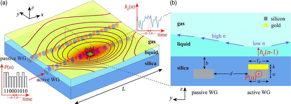
Figure 1.Schematic description of the key components in the integrated optofluidic system under study describing the underlying mechanism of the light–liquid interaction and the memory used for RC. (a) 3D perspective presenting a box-shaped liquid cell of length
2 Methods
2.1 Details of Multiphysics Simulation
To capture the complex coupling between light propagation, fluid dynamics, heat transport, and surface tension effects, we employed finite-element-based commercial software COMSOL Multiphysics®27 with Wave Optics, heat transfer, and CFD module, where changes of thin liquid film geometry are simulated by the moving mesh method. Since electromagnetic dynamics occurs on much shorter time scales compared to other processes we consider, the optical simulation is performed in the frequency domain, whereas all other processes are simulated in the time domain. For the WG and thinner gold patch, we use a free tetrahedral mesh resulting in mesh elements and degrees of freedom. These memory demanding simulations are performed on a constructed dedicated server with 16 cores and 512 GB memory; for instance, the single self-induced phase change simulation presented in Fig. 2 takes more than 24 h simulation time. The governing equations, matching and boundary conditions, as well as key parameters used for the simulation, are provided in the Supplementary Material. In all simulations, we assume the initial liquid surface is flat and forms a contact angle with a value of 90 deg with the vertical silica boundary walls.
Sign up for Advanced Photonics TOC. Get the latest issue of Advanced Photonics delivered right to you!Sign up now
2.2 Details of RC Simulation
Construction of the computational scheme for optofluidic RC involved three main steps. In the first step, we employed 3D simulations, each providing gas–liquid interface deformation under an equivalent heat source (see Fig. S4a in the Supplementary Material) for a variety of different developed temperatures in the gold patch and initial configurations (see Fig. S3 in the Supplementary Material). In the second step, we extracted the corresponding data describing evolution of and performed linear fitting to derive the following reduced phenomenological one-dimensional (1D) model for :
To finalize the computation result, the output vector is subjected to the threshold step with values above (below) 0.5 being rounded to one (zero). The corresponding error rate () is then determined by comparing the computation result after the threshold with the true result, leading to
3 Results
3.1 Nonlinear Self-Induced Phase Change
Consider a single Si channel WG with integrated gold patch, covered with thin liquid film shown in Fig. 2(a). Following the mechanism described above, the gold patch serves as an optical heater, which induces TC-driven flows and deformation of the liquid dielectric film. In our simulations, we set liquid properties close to silicone oil, which is an optically transparent and highly nonvolatile liquid, thus appropriate for future experimental realizations; see Table S1 in the Supplementary Material for simulation parameters.
![]()
Figure 2.Numerical multiphysics simulation results presenting self-induced phase change in a single active WG covered with a thin liquid film. (a) Deformed gas–liquid interface under 0.1-mW CW light-induced TC effect at time
Figure 2(a) presents simulation results of the self-induced phase change effect due to the TM mode propagating in a single active WG covered with a thin liquid dielectric film of the initial thickness of 500 nm. In particular, Fig. 2(a) presents the corresponding deformation and temperature field of the gas–liquid interface at time after the 0.1 mW continuous wave (CW) mode began to propagate in the WG, whereas Fig. 2(b) presents the gas–liquid deformation as a feedback response (circular arrow), allowing us to store information and affect subsequent optical pulses at the same compact spatial region without the need of dedicated large footprint optical feedback elements, e.g., optical rings.31 The colormap describes electric field intensity at and thin liquid-deformation along the plane, where is the propagation direction; note the effect of light reflection from the gold patch leading to distortion of the incoming mode. Figure 2(c) presents the electric field intensity at two different times along the planes , , and , where is the center of the gold patch. Specifically, the images at the first row indicate that at , i.e., prior to liquid film deformation, the incident TM mode experiences reduction in intensity but preserves its TM polarization. However, once the liquid film begins to deform, the second row indicates that after 20 ms the incident mode changes its shape due to superposition with the reflected wave from the gold patch, and the transmitted mode is no longer top-bottom symmetric. Figures 2(d)–2(g) present the self-induced phase change, deformation of the thin liquid film above the gold patch center (i.e., at region of minimal thickness just above the center of the gold patch), average temperature of the gold patch , and the corresponding transmittance as a function of time, respectively, under various optical powers. Naturally, increasingly higher power levels and accompanying temperature gradients lead to more significant and the corresponding self-induced phase change effects. Interestingly, at optical powers of 0.1, 0.07, and 0.05 mW, the corresponding liquid film deformation also induces prominent transmittance change, leading to a power reduction by approximately a factor of 2/3, which we attribute to impedance mismatch created by the liquid deformation. Notably, owing to the relatively low power levels required to activate TC-driven film thinning as well as the large refractive index contrast across the gas–liquid interface, sufficiently thin liquid film with high overlap of the evanescent optical tail with the gas phase supports a few orders of magnitude higher self-induced phase change compared with that of the thermo-optical (TO) effect. In particular, Fig. S1 in the Supplementary Material indicates that the system described in Fig. 2(a) admits approximately three orders of magnitude higher self-induced phase change compared with a similar system, where instead of liquid film one employs a dielectric solid material which does not support the TC effect. It is worth mentioning that due to the moving mesh method employed in the multiphysics software,27 the simulation terminates once the gas–liquid interface reaches the few elements thick film, as measured from the bottom of the liquid cell, leading to a phase change of . In future experimental realizations, which are not subject to such limitation, we expect to obtain even higher values of self-induced phase change and nonlocality scales, as well as self-induced transmittance/reflection modulation, shortly described below. Furthermore, given the fact that liquid deformation is mainly concentrated around the compact gold patch, based on our study, the size of the liquid cell can be, in principle, reduced to , whereas higher values of self-induced phase change can be achieved by placing several gold (or other metal) patches along the WG.
3.2 Nonlocal Effect
Consider the optofluidic components schematically presented in Fig. 3 and analyze the effect of the self-induced TC-driven deformation on modes in the two WGs as a function of their distance . In particular, we consider close and far separation regimes characterized by and , respectively, where is the corresponding evanescent scale of the TM mode. To investigate the close separation regime, we focus on the directional coupler geometry32 with minimal distance presented in Figs. 3(a) and 3(b), whereas in the far separation regime we consider parallel WGs geometry presented in Figs. 3(d) and 3(e). Figure 3(c) shows the simulation results of the TM mode injected only into the active WG, indicating a decrease of the coupling coefficient as a function of liquid deformation, leading to decreased (increased) transmittance of the TM mode through the passive (active) WG as a function of time. In case the distance between the WGs is several microns (), we can increase the nonlocal effect of the active WG on the passive WG by increasing the transverse dimension of the gold patch , which facilitates more efficient heat transport and enables liquid film deformation profile, which extends toward the passive WG. This approach also allows us to alleviate the simulation limitation taking place due to its termination once the liquid film reaches a thickness of a few elements. Figure 3(d) presents 3D thin liquid film deformation and the underlying temperature map for the case, whereas Fig. 3(e) presents a normal cross section with the computational result of the corresponding modal structure. In particular, the latter presents numerical results at time of two different simulations when the light was injected into the active or passive WGs and indicates that the gold patch does not guide surface plasmon polaritons from one WG to another. Figure 3(f) presents the associated phase change in the passive WG as a function of time for three different separations, naturally indicating smaller values of phase shift for increasingly larger separations. Note that in contrast to the close separation regime, an initially low power (which is not sufficient to deform the liquid film) optical TM mode was also injected into the passive WG to analyze its evolution under he effect of the higher power mode in the active WG. Notably, the maximal separation between the WGs is much higher than the corresponding evanescent scale and also significantly exceeds other known optical nonlocality scales stemming from alternative optical nonlinearities, such as photorefraction,33 TO effect,34,35 and long range molecular interaction between liquid crystals molecules.36
![]()
Figure 3.Numerical results demonstrating self-induced nonlocal interaction between two adjacent WGs in (a)–(c) the close and (d)–(f) far separation regimes, due to continuous TM mode of wavelength 1550 nm injected to the active WG leading to TC-driven deformation of the liquid film; geometric parameters of WGs and the gold patch are provided in
3.3 Self-Induced Transmittance and Reflection in Channel Bragg Waveguides
Consider the SiN Bragg WG on silica substrate presented in Fig. 4, where some of the ribs are covered with a gold patch of thickness . Here, we employ SiN rather than Si because the former has a lower refractive index (2 at wavelength 1550 nm) leading to larger mode volume and thus to higher sensitivity of perturbations in the geometry of the gas–liquid interface. First, we design the periodic WG to admit a stop-band at a wavelength 1550 nm when it is covered with a thin liquid film of thickness (as measured from silica substrate) and admit non-zero transmittance without the thin liquid film. The evanescent penetration of the incident light a few periods into the SiN Bragg WG, which is inherent to stop-band conditions, triggers heating of the gold patches close to the input facet (left), which in turn triggers TC-driven deformation of the liquid film. As liquid thickness becomes thinner near the input facet, the designed propagation conditions facilitate deeper penetration of the optical mode into the periodic structure, thus leading to film thinning above more distant regions from the input region, which in turn amplifies the process. Indeed, Fig. 4(c) presents an initially flat gas–liquid interface at , liquid deformation with indentation closer to the input facet at , and wider indentation over the central part of the periodic structure at the later time of , leading to almost minimally thin liquid film above all WG ribs. Similarly, a periodic structure with slightly different period can be designed to support propagation once the WG is covered with liquid film and a stop band once the liquid film is replaced by air. Following the same arguments as above, self-induced liquid thinning over the periodic structure is expected to shift the propagation conditions and lead to lower transmittance, as indeed described by the blue curve in Fig. 4(d). Interestingly, the presented effects are reminiscent of electromagnetically induced transparency, which relies on a very different phenomenon, where quantum interference allows the propagation of light through an otherwise opaque atomic medium.39
![]()
Figure 4.Numerical simulation results of the self-induced transmittance and reflection effects. (a) The underlying 3D geometric setup of the periodic SiN Bragg WG on silica substrate and (b) the corresponding 2D normal cross section in the
3.4 Reservoir Computing of Digital and Analog Tasks
Consider Fig. 5(a) describing an MZI circuit with two directional couplers and an optofluidic cell in one of the arms, which supports the nonlinear self-induced phase change effect described above, and the circuit described by Fig. 5(c) with a liquid cell placed in the coupling region, which affects the transmittance via self-induced coupling change (nonlocal effect). In both cases, the self-induced phase/coupling change due to liquid deformation invoked by the active WG is translated into intensity changes in the output arms and . To allow sufficiently large actuation of the liquid, the corresponding actuation time scale () must be smaller than pulse width (), whereas to ensure memory, i.e., that the liquid deformation imprinted by the ()th bit will affect the phase/coupling change of the th bit, the distance between subsequent pulses () must be smaller than . Both conditions can be summarized as
![]()
Figure 5.Simulation results presenting RC computing of the XOR task by employing self-induced phase change (nonlinear) and self-induced coupling change (nonlocal) effects. (a) Schematic diagram presenting the MZI circuit with two linear couplers, where the liquid cell introduces self-induced phase change in one of the arms measured by a pair of detectors
3.4.1 Digital task
Consider the delayed XOR operation, where an arbitrary input time series () of zeros and ones is mapped to output sequence according to
To implement XOR operation, we can either employ the (nonlinear) self-induced phase change or the (nonlinear–nonlocal) self-induced coupling change with circuits Figs. 5(a) and 5(c), respectively. The input series is encoded as a sequence of square pulses of power level or depending on the value of logic “0” or “1,” as described by Fig. 5(b); the corresponding power level operates during a time and is followed by relaxation time . Figures 5(d) and 5(e) present the performance diagram with different colors encoding the corresponding prediction error, for the case of nonlinear circuit and nonlocal circuit described by Figs. 5(a) and 5(c), respectively. Note that the performance diagram of the nonlocal circuit presents the (white) region of vanishing error, which has a larger area compared with the corresponding area in the performance diagram of the nonlinear circuit. Furthermore, the lowest power value of the white region in the nonlinear case is with a lower value around for the nonlocal case. Higher performance of the nonlocal circuit stems from higher sensitivity of the intensity of the transmitted signal with respect to changes of the liquid thickness, compared with the nonlocal case. Specifically, sensitivity estimates can be determined by taking the derivative of the MZI signal due to a phase shift , given by , where the derivative can be estimated from Fig. S5c in the Supplementary Material; similarly, Fig. S7 in the Supplementary Material provides an estimate for the typical slope/sensitivity in the nonlocal case. The enhanced performance of the nonlocal circuit for the delayed XOR task manifests also for the XOR task, as can be seen by comparing the corresponding performance diagrams of the nonlocal circuit with minimal error of , presented in Fig. 5(f), to the performance diagram of the nonlinear circuit presented in Fig. S6c in the Supplementary Material with minimal error of . In general, as can be seen from the graph in Fig. S6d in the Supplementary Material, presenting the test error for a fixed and , performance of the XOR gate quickly degrades for higher values of the delay , which also demonstrates prominent memory of only one time backward in time. The underlying dynamics of the thin liquid film was obtained by constructing a reduced 1D model, which was obtained from analyzing numerous 3D multiphysics simulations27 results, where the thin liquid film was subjected to various initial conditions and actuation powers. In our reduced model, the transient dynamics of the thin liquid film is subject to the first-order ordinary differential equation with power dependent coefficients, allowing a simple numerical scheme to predict the accompanying phase/coupling change and the resultant power levels at the detectors (see Sec. 2 and the Supplementary Material). In particular, Figs. S3, S5a, and S5c in the Supplementary Material present as a function of time for several different initial thicknesses and input powers, the relation between and and the one-to-one relation between and the induced phase shift, respectively, whereas Fig. S7 in the Supplementary Material presents transmittance values as a function of optical power in the active WG. Figure 5(g) presents the underlying dynamics of the thin liquid film (red curve) and the output signal (blue curve) in the detector in the nonlocal circuit [Fig. 5(c)], under an exciting signal (green curve). To visually analyze the different patterns of detected power, we construct folded dynamics diagrams, where the optical signals at different time intervals of length are plotted on top of each other. Figures 5(h) and 5(i) present folded dynamics graphs for the nonlinear and nonlocal circuits between times to , respectively, where the signal in the nonlocal circuit shows enhanced separability compared to the nonlinear case performed under similar conditions , , and . Interestingly, Figs. 5(h) and 5(i) do not show dependence on initial conditions, which is in concert with the graph in Fig. S6a in the Supplementary Material, demonstrating that the system practically “forgets” the initial conditions after and, furthermore, showing the emergence of patterns that are characteristic of particular dynamics and actuation signals. For instance, Fig. 5(i) presents four main curves with an internal substructure, corresponding to “1” or “0,” which was preceded by “1” or by “0.” These represent the four dominant combinations, which allow an efficient solution of the delayed () XOR task, whereas the internal structure represents next order memory effects, which allows us to some extent to solve the XOR task. More formally, since the dynamics of our system converges to states that do not depend on the initial conditions, it satisfies the so-called common-signal-induced synchronization (see Ref. 40 and references within), also known as echo state,8 which is a necessary property enabling a dynamical system to serve as an RC. To determine the required optical energy needed for training, we assume that the number of “0” and “1” pulses is equal, leading to ; for instance, , , and yields . Similarly, the energy during the test stage , required for a solution of a string of length , is given by . The case with and similar parameters used during the training stage discussed above yields .
3.4.2 Analog task
Next, we consider the classification task of hand-written “zero” and “one” digits; Fig. 6(a) presents a sample of 20 images from Modified National Institute of Standards and Technology (MNIST) database,41 each of the size . To encode each image as a signal, without filtering or other preprocessing procedures, we partitioned the image into a set of horizontal rows or columns, where each pixel is represented by a 1-ms long constant optical power proportional to the brightness value of the corresponding pixel. Specifically, the pixels are encoded according to power values , where is the power needed to encode the brightest pixel of unity brightness (), whereas corresponds to dark pixels that carry no features, and other values correspond to pixels of intermediate brightness. Figure 6(b) presents an example of a hand-written “one” digit used for classification, where the 28 ms long signal encoding the highlighted red horizontal row is given by Fig. 6(c) with left/right pixels corresponding to early/late times. To perform image classification, we employ either the nonlinear or nonlocal circuits presented in Figs. 5(a) and 5(c), respectively, where the top and the bottom arms receive in parallel the 1-ms long bits encoding the th and the following ()th rows, respectively, thus generating more correlations between different lines and leading to higher accuracy compared to feeding just one arm at a time. Figure 6(d) presents the classification error during the training and testing stages, with training values naturally admitting lower values. Interestingly, both errors admit fairly low values below 0.5% across a wide range of power values spanning from 0.01 to 0.1 mW. The total energy needed to feed one image is determined by , where is the average brightness level of the image laying between and typically admitting value . The corresponding energy for the training/testing stage is achieved by multiplying the one image energy above by the total number of corresponding images (see Sec. 2); for , the corresponding average power level is given by . Importantly, the single liquid cell circuits in Figs. 5(a) and 5(c) can be extended to form a more complex network. For instance, Fig. S9 in the Supplementary Material presents a network consisting of four inputs, two liquid cells, and two detectors. While it does not present enhancement in accuracy, it allows us to reduce the computation time by a factor of two without increasing the total required energy. Analyzing networks with more inputs, allowing us to achieve optimization of the handwritten digits recognition task and further reduction in operation time is beyond the scope of this work.
![]()
Figure 6.RC of analog task: classification of hand-written “zero” and “one” digits. (a) Sample of 20 images each of size
To learn more about the role of the reservoir in our modality, we also performed linear regression analysis, where the output signal is made equal to the input signal, which is followed by ridge regression, allowing us to obtain the corresponding weights that perform the corresponding task with corresponding error given by 0.61%. Interestingly, employing a reservoir presented in Fig. 5(a) but without liquid response yields similar 0.61% performance for “zero/one” digits classification, which is around 4.3 times higher compared to the highest 0.14% reservoir performance for this task. It is worth mentioning that the performance described in Fig. 5(d) and Fig. S8 in the Supplementary Material is not a prominent function of the optical power and using larger power does not lead to significantly enhanced performance. While in this work the input data used for the analog task were not subject to any preprocessing, we expect that common methods such as edge detection should improve the accuracy.
4 Discussion
To summarize, we believe that the family of physical effects predicted to take place due to nonlinear–nonlocal interaction between thin liquid film and channel WG modes in integrated chip-scale photonics platforms, and the emergent concept suggested to employ these effects to realize optofluidic RNN supporting RC applications, will stimulate both pure light–matter interaction studies and development of RNN architectures/schemes. In particular, our 3D simulation results, which take into account optical propagation with losses, heat transport, and fluid dynamics as well as the underlying surface tension physics, indicate that the magnitude of the self-induced phase change due to the TC effect in the liquid film is approximately three orders of magnitude higher compared to the more common heat-based TO effect. Therefore, the predicted effects of self-induced coupling change and self-induced bandstructure and transmittance change can stimulate experimental and theoretical studies validating the predictions and exploring bandstructure tuning in photonic crystals and their topological properties,42,43 as well as studying nonlocal interaction between a large number of WGs, even if their separation exceeds the optical evanescent scales. While in our work, we employed a gold patch due to its optical absorption properties, studying metal structures designed to support resonant absorption due to surface plasmon polariton oscillations is another intriguing possibility capable of inducing and modifying resonant absorption in channel WGs, as we briefly mention in Fig. S11 in the Supplementary Material. From the ML-based perspective, the employed self-induced phase/coupling change allows us to achieve nonlocal–nonlinear interaction and memory at the same compact actuation region and perform the digital XOR and analog handwritten images classification tasks, which can lead to new RNN elements and architecture that take advantage of the built-in internal feedback capability. Notably, our work demonstrates for the first time that controlled deformation of the gas–liquid interface on the submicron scale can operate as an RNN, which can be extended to a network with a larger number of liquid cells (or a larger number of WGs in a single liquid cell) and further provides design principles of compact optofluidic and complementary metal–oxide–semiconductor compatible optofluidic RC systems, which are capable of inducing additional nonlinearity beyond the commonly employed square-law detection, without utilizing optical resonant structures, and furthermore operates under a wide range of conditions that do not require phase matching conditions. In particular, our design of an optofluidic-based RC system is capable of leading to 4–5 orders of magnitude reduction in size compared to previous liquid-based RC44,45 systems and also to a few orders of magnitude faster computation compared to the surface waves dynamics and reaction-diffusion processes, which were employed in Refs. 44 and 45, respectively. While the presented optofluidic approach for RC requires more energy compared to the present state-of-the-art approaches such as the opto-electronic based method, offering modulation rate with hundreds of fJ per bit46 (see Table S2 in the Supplementary Material), we should keep in mind that the electro-optic approach requires an external modulation unit, whereas in the optofluidic approach the modulation is internal due to the specificity of the gas–liquid interaction. In particular, internal feedback allows us to invoke nonlinearities and memory effects in the interaction region and thus translates into a very compact computation region without feedback loops, which are required in systems that employ external feedback. It is not clear how to achieve a self-induced refractive index response of the order with the electro-optic effect, though self-induced modulation can be achieved by employing two-photon absorption and other nonlinearities31 using significantly higher power levels compared with state-of-the-art externally modulated mircoring resonator devices.46 Furthermore, we should keep in mind that neural brain activity also occurs on a ms time scale and is based on several ionic transport processes, which also take place in a liquid environment. Therefore, even if our study in its current version cannot suggest computational capabilities comparable to that of a human brain, the general strategy of combining several different physical processes rather than relying on a small number of physical effects may prove to be a useful strategy to achieve more efficient computational approaches. It is worth mentioning that while phase-change materials, where optically induced phase change between crystalline and amorphous phases invokes self-induced transmittance change, were recently employed for NC applications,47
Chengkuan Gao received his BSc degree in physics from Wuhan University in 2017 and his MSc Eng. in materials science from University of Pennsylvania in 2019. He is currently a PhD student in the Ultrafast & Nanoscale Optics (UNO) Group, majoring in photonics at the Department of Electrical and Computer Engineering (ECE) at University of California, San Diego.
Prabhav Gaur received his BTech degree in electrical engineering from the Indian Institute of Technology Kanpur in 2019 and his MS degree in electrical and computer engineering (photonics option) from University of California, San Diego (UCSD) in 2021. Currently, he is pursuing his PhD in electrical and computer engineering (photonics option) from the UCSD, and his research interest includes optical signal processing and optical metrology.
Shimon Rubin received his BSc and MSc physics degrees from Technion – Israel Institute of Technology in 2001 and 2004, respectively, and his PhD physics degree from Ben-Gurion University of the Negev in 2012. Between 2013 and 2016 he served as a postdoctoral fellow in the Department of Mechanical Engineering at Technion, and in 2017 he joined as a postdoctoral researcher and later as assistant project scientist in ECE at UCSD.
Yeshaiahu Fainman received his MSc and PhD degrees from Technion, Israel, in 1979 and 1983, respectively. He joined the ECE Department at UCSD in July 1990, following a faculty appointment at the University of Michigan, and now serves as a Cymer chair and distinguished professor, directing the Ultrafast and Nanoscale Optics Group in research of nanophotonics. He has contributed over 280 manuscripts and 450 conference proceedings and is a fellow of OSA, IEEE, and SPIE, and a recipient of numerous prizes and awards.
References
[1] M. Borghi et al. Nonlinear silicon photonics. J. Opt., 19, 093002(2017).
[7] H. Jaeger. The echo state approach to analysing and training recurrent neural networks—with an erratum note(2001).
[14] P. R. Prucnal, J. S. Bhavin, M. C. Teich. Neuromorphic Photonics(2017).
[24] V. G. Levich. Physicochemical Hydrodynamics(1962).
[28] G. Montavon, M. Lukoševičiuset?al.. A practical guide to applying echo state networks. Neural Networks: Tricks of the Trade, 659-686(2012).
[29]
[30] S. Chatterjee, A. S. Hadi. Regression Analysis by Example(2013).
[32] G. Lifante. Integrated Photonics: Fundamentals(2003).
[39] R. Boyd. Nonlinear Optics(2008).
[40] K. Nakajima, M. Inubushi, I. Fischer et al. On the characteristics and structures of dynamical systems suitable for reservoir computing. Reservoir Computing: Theory, Physical Implementations, and Applications, 97-116(2020).
[41] Y. LeCun. The MNIST database of handwritten digits(1998).
[43] T. Ozawa et al. Topological photonics. Rev. Mod. Phys., 91, 015006(2019).

Set citation alerts for the article
Please enter your email address
© Copyright 2018-2021 | Chinese Laser Press. All Rights Reserved 沪ICP备15018463号-20