
Zhengji Xu, Nanxi Li, Yuan Dong, Yuan Hsing Fu, Ting Hu, Qize Zhong, Yanyan Zhou, Dongdong Li, Shiyang Zhu, Navab Singh. Metasurface-based subtractive color filter fabricated on a 12-inch glass wafer using a CMOS platform[J]. Photonics Research, 2021, 9(1): 13
- Photonics Research
- Vol. 9, Issue 1, 13 (2021)
Abstract
1. INTRODUCTION
Color filters, as essential optical components, have been widely applied in color display, imaging, sensing, hologram projection, photovoltaic devices, and optical measurement systems [1–9]. Traditional dye-based color filters work based on the wavelength-selective optical absorption/reflection of the chemical bonds, having issues including environmental hazards and performance degradation under high temperature or exposure to ultraviolet radiation. With advances in nanotechnology, the emerging structural color filters have drawn a lot of interest [10–19]. This kind of color filter works based on the interaction between incident light and nanostructures (e.g., Mie resonances [3,20–22]) to achieve wavelength-dependent optical absorption/reflection, and hence can overcome the drawbacks of traditional dye-based color filters. Furthermore, its fabrication can be done using state-of-the-art complementary metal-oxide-semiconductor (CMOS) compatible fabrication facilities, which are currently used in the microelectronics industry. Various functional photonics devices have been demonstrated based on fabrication lines compatible with the infrastructure of CMOS platform for optical communication [23–25], chemical gas sensing [26–28], optical frequency synthesis [29,30], light detection and ranging [31–33], etc. Contributed by the photolithography patterning technology, the fabrication of these devices is scalable to large areas, and suitable for mass production. Recently, such fabrication lines were also used to demonstrate metasurface-based devices [34–42], which contain a single metasurface layer with nanostructures of subwavelength scale.
Structural color filters with narrow passbands contributed by the periodic pillar or hole structure have been widely studied in the past two decades since the first report of extraordinary optical transmission of a periodic metallic subwavelength scale array [43]. The passband of the additive color filter (ACF) can be designed by tuning the period, pitch, or dimension of subwavelength structures [44]. The ACFs formed by both metallic and dielectric subwavelength nanostructure arrays have been recently demonstrated, working in either transmission mode or reflection mode [1,2,6,45,46]. However, the ACF has relatively lower transmission/reflection efficiency compared with its counterpart, the subtractive color filter (SCF), since most of the light in the spectrum is filtered out. SCFs can achieve higher transmission/reflection efficiency since they work based on the removal of the complementary color within the frequency spectrum to achieve the color filtering effect [47–50]. Although the transmission/reflection efficiency can be improved significantly for both ACF and SCF by using the metal–insulator–metal (MIM) or metal–dielectric (MD) resonant structure [12,51–54], the multi-layer structure adds fabrication complexity and hence is not suitable for device mass production and integration with other devices. Meanwhile, color filters fabricated on a CMOS-compatible platform in large scale for mass production on glass wafer substrates remain unexplored.
In this work, we demonstrate SCFs fabricated on 12-inch (300-mm) glass wafer substrates using the CMOS-compatible fabrication process. In order to make transmissive SCFs on transparent glass substrates, the glass wafer handling issue in fabrication tools has been resolved by a layer transfer process developed in house. Three batches of wafers are fabricated with variation in pillar height to investigate the relation between SCF performance and pillar height. Functional SCFs with different colors are demonstrated, and the displayed colors are verified by matching the complementary color of filtered colors within a red-yellow-blue (RYB) color wheel. The magnetic dipole resonance is found from the simulation. The transmittance spectra obtained from the simulation and experiment are compared and discussed. The work paves the way towards large-scale mass production of structural color filters.
Sign up for Photonics Research TOC. Get the latest issue of Photonics Research delivered right to you!Sign up now
2. DEVICE DESIGN AND FABRICATION
A three-dimensional (3D) schematic of the transmission-mode SCF on glass is shown in Fig. 1(a). The metasurface is composed of an array of embedded amorphous-Si (a-Si) nanopillars with a fixed diameter of 105 nm, and varied pitches of , , and . These three pitch sizes are designed for the metasurface-based display letters “I,” “M,” and “E,” respectively, and their corresponding resolutions are around 100,000 dots per inch (dpi), 84,000 dpi, and 72,000 dpi, respectively. Figures 1(b)–1(d) are the side, top, and perspective views of the a-Si nanopillar on a glass wafer for the design and simulation. There are three heights of a-Si nanopillars in our design—110, 170, and 230 nm—to investigate the relationship between embedded a-Si nanopillar height and SCF’s performance.
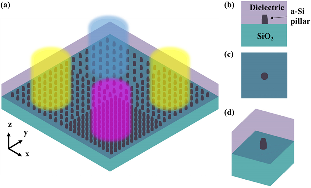
Figure 1.Schematic of the metasurface-based SCF function device and single nanopillar as metasurface unit cell. (a) Schematic of the SCF illustrating the color filter effect (drawing not to scale). (b) Side view, (c) top view, and (d) perspective view of the a-Si nanopillar on glass wafer for SCF design and simulation.
The fabrication was done on the Institute of Microelectronics (IME)’s 12-inch (300-mm) wafer platform for flat-optics [55]. To realize the SCF design, the Si wafer transfer technique on a glass wafer is developed. The Si wafers with a layer on top are used as substrates. Then different thicknesses of a-Si films are deposited by the plasma enhanced chemical vapor deposition (PECVD) method. The a-Si nanopillars are then patterned by a 193-nm ArF immersion scanner, followed by reactive ion etching. The patterned a-Si layer is then transferred from the Si wafer to a glass wafer through a bonding glue assisted layer transfer process. The a-Si nanopillars are embedded in the bonding glue, as shown in Fig. 1. The bonding glue is a transparent dielectric material with a refractive index close to silica. More details on the wafer fabrication can be found in Appendix A.1 as well as in Ref. [42].
A photograph of the fabricated 12-inch (300-mm) glass wafer with the central die highlighted by a blue dotted line is illustrated in Fig. 2(a). The observation of the blue color A*STAR logo at the back shows the transparency of the glass wafer in the visible wavelength range. The zoomed-in images of the central die from wafers with a-Si layer thickness variation are illustrated in Figs. 2(b)–2(d), in which the SCF devices are highlighted by blue-dotted lines. The heights of the a-Si pillars are close to 110, 170, and 230 nm in Figs. 2(b)–2(d), respectively. It can be observed that the colors of the “IME” letters are different under pillar height variation. The corresponding transmission electron microscopy (TEM) images of single nanopillar are illustrated in Figs. 2(e)–2(g), respectively. It can be observed that the edges of the nanopillars have rounded shapes instead of sharp corners, which could be due to over-etching. A sharp corner can be achieved by optimizing the a-Si etching process, such as reducing the etching power or time.
![]()
Figure 2.Fabricated glass wafer, single dies, and single nanopillars with different heights. (a) Photo image of 300-mm glass wafer, with blue dotted line highlighting the central die. (b)–(d) Photo images of central die (from different wafers) after wafer dicing with a-Si pillar height design of (b) 110 nm, (c) 170 nm, and (d) 230 nm, respectively. Each die has a size of 26 mm × 33 mm. SCF device is highlighted using blue dotted line in each die, showing different displayed colors under different pillar heights. (e)–(g) Transmission electron microscopy (TEM) images of the fabricated a-Si nanopillar with height close to (e) 110 nm, (f) 170 nm, and (g) 230 nm.
3. RESULTS AND DISCUSSION
The simulated and measured transmittance spectra of the nanopillar array for SCF in the wavelength range of 400 to 800 nm under various pillar heights and pitches are shown in Fig. 3. The simulation is conducted by using the 3D finite difference time domain (FDTD) method (FDTD Solutions, Lumerical Inc. Vancouver, British Columbia, Canada), with periodic boundary conditions along and directions. The pillars with truncated shapes at the top are used in the simulation model. The pillar heights are set to be 110, 170, and 230 nm. The pillar diameter at the bottom is fixed at 105 nm. The broadband visible light polarized in y-direction is launched from the glass substrate below and propagates towards the nanopillar located on the substrate (propagating from to direction). As illustrated by the red line in Fig. 3, the simulated spectra have relatively low transmission in a short wavelength range (400–600 nm) compared with a long wavelength range () due to the resonance of the electromagnetic wave within the pillar structure. The resonance modes will be discussed in detail later.
![]()
Figure 3.Simulation and experiment results of SCF with different pillar heights and pitches. (a)–(i) Simulated (red line) and measured (blue line) transmittance spectra of the color logo “IME” under various pillar heights (
The SCF devices are experimentally characterized using a microscopic spectrometer measurement system, with incident visible light from a mercury lamp injected from the bottom, and the transmitted light is captured by an optical spectrometer at the top. A charge-coupled device (CCD) camera is also placed at the top for device monitoring and alignment purposes. Its schematic is provided in Fig. 6 (Appendix A.2). The measured transmittance spectra of the SCF with nanopillar heights of 110, 170, and 230 nm and pitches of 250, 300, and 350 nm in the wavelength range of 400 to 800 nm are also plotted in blue lines in Figs. 3(a)–3(i). The insets within these figures include color photos of fabricated SCFs, taken from the highlighted areas in Figs. 2(b)–2(d). Taking Figs. 3(a)–3(c) as examples, different from the additive color system, the as-measured wavelength valleys do not represent the colors of blue, green, and yellow, but their complementary colors: orange, red, and purple. The appearance of the colors of the “IME” letters can be verified by the RYB color wheels, which are also included as insets. In each color wheel, the transmittance minimal color points towards its complementary color, which is the displayed color of the metasurface device. Also, it can be observed that the transmittance of SCF is above 90% in a long wavelength range (). Most of the photons pass through the SCF except for the selective wavelength range, leading to a higher transmission in comparison with ACF.
In addition, from the experimental results in Figs. 3(a)–3(i), as the pillar height increases, the transmittance at the designed resonant wavelength decreases, which leads to higher power distinction between the resonance and non-resonance spectrum range, and hence better displayed color contrast. Such a contrast increase can be visualized by comparing the insets of the “IME” logo in Fig. 3. For the SCF functional device, it is expected to have low transmission at the filtered wavelength, so that high display contrast can be obtained. Hence, future work can be committed to further reduce the transmission of SCFs at the filtering wavelength by optimizing the device design, especially for pillars with lower height.
The experimental spectra measured from the devices match with the simulation spectra in Fig. 3 in general. The discrepancy of resonance wavelengths in Figs. 3(b), 3(g), and 3(i) is contributed mainly by the pillar diameter variation after the etching process. Such a discrepancy can be offset by adjusting the diameter of the nanopillar within the range of in simulation, which is the diameter variation range generated from the fabrication process. Also, based on the standard International Commission on Illumination (CIE) 1931 color matching function, the simulation and measurement results are plotted and compared in the CIE chromaticity diagram, as illustrated in Figs. 3(j)–3(l). The detailed calculation steps are also included in Appendix A.3.
In order to visualize these resonance modes mentioned earlier, the field distributions of the nanopillars with bottom diameter of 105 nm and pitch of 250 nm under different heights are captured and illustrated in Fig. 4. The electric and magnetic field distributions for pillar heights of 110, 170, and 230 nm are illustrated in Figs. 4(a)–4(c), respectively. The first and second rows show the top and side views of the field distributions within the nanopillars, respectively. The edges of the nanopillars are shown in the white solid line. Based on the simulated transmittance spectra obtained in Figs. 3(a)–3(c), the resonance wavelengths are selected to be 550, 572, and 580 nm under pillar heights of 110, 170, and 230 nm, respectively. From the electric field distribution of the nanopillar (side view), as shown in the second row of Fig. 4, the circular electric-field loop can be clearly observed under different pillar heights. Also, from the magnetic field distribution within the nanopillar (side view), as illustrated in the second row of Fig. 4, the magnetic dipole resonance can be clearly seen. Such resonance within the nanopillar cavity contributes to the low transmission at the corresponding wavelength.
![]()
Figure 4.Simulated electric and magnetic fields of nanopillar under different pillar heights. (a)–(c) Electric and magnetic field distributions at resonance wavelengths of (a) 550 nm, (b) 572 nm, and (c) 580 nm for a-Si nanopillars with heights of 110, 170, and 230 nm, respectively. Pillar pitch and bottom diameter are fixed at 250 and 105 nm, respectively. The wavelengths are selected based on the resonance of the transmittance spectra from simulation shown in Figs.
Furthermore, in order to verify that the SCF is able to cover the whole visible wavelength, an additional simulation is conducted, with the results shown in Fig. 5. The pillar height of 230 nm is used based on the existing wafer that has been fabricated. The pillar pitch and diameter are varied. Figure 5 shows the selected simulation curves, with pillar pitch and diameters indicated in the legend, showing the filtered wavelength being able to cover the whole visible wavelength regime.
![]()
Figure 5.Simulation results of SCF with pillar height of 230 nm under different pillar diameters (
4. CONCLUSION
In summary, metasurface-based SCFs on 12-inch (300-mm) glass wafers are demonstrated using a-Si as the metasurface layer. To make the transmissive-type SCF on a transparent glass wafer substrate, an in-house developed layer transfer process is used to solve the glass wafer handling issue in fabrication tools. Three batches of wafers with pillar height variation are fabricated using a CMOS-compatible process. The effect of a-Si nanopillar height on the device transmittance spectra is investigated through both simulation and experiment. The transmittance spectra of the SCF from the simulation and experiment are compared and discussed. The discrepancies between the simulation and experimental results are mainly due to the diameter variation from the fabrication. The displayed colors of the fabricated devices are verified by matching the complementarity of the color at the resonance of the measured transmittance spectra in the RYB color wheel. By utilizing the CIE 1931 color matching function, the chromaticity coordinates of transmittance spectra for SCFs are plotted. The work paves the way for mass production of large-area flat-optics components on glass wafer substrates.
APPENDIX A: METHODS
A.1. Wafer Fabrication Process
The wafer-level fabrication process starts with a silicon wafer substrate with 12-inch (300-mm) diameter. A PECVD layer with 1 μm thickness is deposited on top, serving two purposes: (1) as an etch-stop layer for the later Si backside etching process; and (2) as a protective cladding layer for the a-Si metasurface layer. Next, a PECVD a-Si metasurface layer is deposited on top of the layer. Three wafers are fabricated using the same method with the a-Si metasurface layer thickness variation of 110, 170, and 230 nm. On top of the a-Si layer, a layer of photoresist is used, followed by the patterning process using state-of-the-art 193 nm deep-ultraviolet immersion lithography. After the photolithography patterning, the etching process is conducted through inductive coupled plasma etching to form the a-Si nanopillars. Following that, a layer of bonding glue is spin coated on the patterned a-Si layer. The material of bonding glue is chosen with a refractive index close to , so that the a-Si nanopillars can be embedded within a more homogenous environment. The fabricated silicon wafer is then flipped upside down and bonded with a 12-inch (300-mm) glass wafer (Corning SG3.4) through the bonding glue layer. Last, the thickness of the silicon substrate on the original silicon wafer is reduced to around 20 nm through a grinding process. The remaining silicon is then completely removed through a wet etching process, using the PECVD layer as an etch-stop layer.
A.2. Microscopic Spectrometer Measurement System
Broadband light from a mercury lamp is incident from the bottom side of the metasurface-based color filter device, as shown in Fig. 6. A 50/50 beam splitter is used to split the light from the metasurface sample into the CCD camera and spectrometer to obtain the optical image and spectrum information, respectively.
![]()
Figure 6.Schematic of microscopic spectrometer measurement system.
A.3. CIE 1931
The CIE 1931 coordinates are calculated using the color matching functions for red, green, and blue colors [2]. First, the overlap integrals between color matching functions with the experimental/simulation transmittance data are calculated using the following three equations:
Acknowledgment
Acknowledgment. The authors thank Dr. Doris Keh Ting Ng for discussion. We extend appreciation to Dr. Qun Ying Lin for support on immersion lithography.
References
[33] J. Notaros, M. Notaros, M. Raval, C. V. Poulton, M. J. Byrd, N. Li, Z. Su, E. S. Magden, E. Timurdogan, T. Dyer, C. Baiocco, T. Kim, P. Bhargava, V. Stojanovic, M. R. Watts. Integrated optical phased arrays: LiDAR, augmented reality, and beyond. OSA Advanced Photonics Congress (AP) 2019 (IPR, Networks, NOMA, SPPCom, PVLED), IM4A.2(2019).
[40] T. Hu, Q. Zhong, N. Li, Y. Dong, Z. Xu, D. Li, Y. H. Fu, Y. Zhou, K. H. Lai, V. Bliznetsov, H.-J. Lee, W. L. Loh, S. Zhu, Q. Lin, N. Singh. A metalens array on a 12-inch glass wafer for optical dot projection. Optical Fiber Communication Conference (OFC), W4C.3(2020).
[41] Q. Zhong, Y. Dong, D. Li, N. Li, T. Hu, Z. Xu, Y. Zhou, K. H. Lai, Y. H. Fu, V. Bliznetsov, H.-J. Lee, W. L. Loh, S. Zhu, Q. Lin, N. Singh. Large-area metalens directly patterned on a 12-inch glass wafer using immersion lithography for mass production. Optical Fiber Communication Conference (OFC), Th2A.8(2020).

Set citation alerts for the article
Please enter your email address
© Copyright 2018-2021 | Chinese Laser Press. All Rights Reserved 沪ICP备15018463号-20