SiGeSn alloys have attracted considerable attention as a versatile group-IV material system for optoelectronic devices. Compared to the group III-V materials, SiGeSn holds advantages on CMOS compatible, low-cost, large wafer size (8-12 inches), high-volume manufacturing, etc. The direct bandgap GeSn as the gain medium is particularly advantageous for achieving the monolithic integration of laser on Si (Fig. 1). The novel laser solution promises a significant advance in Si photonics, which is extensively applied in applications such as data communication and 3D sensing.
Since the first demonstration of optically pumped GeSn laser in 2015, researchers have made substantial improvements on GeSn lasers. The maximum laser operating temperature leaped from the initial 90 K to near room temperature. The reduction on threshold made it possible for continuous-wave operation. Various laser geometries were studied, including ridge waveguide, micro disk, photonic crystal, and micro-bridge. The lasers were further developed into advanced structures such as double-heterostructure and multiple quantum well. However, all the progress was made under the optically pumping scheme.
On the path towards the electrically injected GeSn laser diode, one may encounter many challenges. The most sensible one is the carrier injection mechanism. Different from the optically pumped lasers, the electrons and holes are injected separately by doping in a laser diode. Until 2020, the multi-institution research team led by University of Arkansas professor Shui-Qing (Fisher) Yu demonstrated the first electrically injected lasers by recognizing such difference and made substantial considerations on the structure design to prevent the hole leakage. The understanding of the GeSn laser diodes has just started.
Yiyin Zhou, the doctoral student in Yu's research group, together with his colleagues, evaluated the laser diode performance with the change of layer thickness and material. The study involves three groups of comparison experiments using GeSn/SiGeSn double heterostructure. Among all devices in this work, the maximum lasing wavelength was measured at 2682 nm at 90 K (Fig. 2). Related results were published in Photonics Research Vol 10, No. 1, 2022 (Yiyin Zhou, Solomon Ojo, Chen-Wei Wu, et al. Electrically injected GeSn lasers with peak wavelength up to 2.7 μm[J]. Photonics Research, 2022, 10(1): 01000222).
First, the lasers with different cap layer thickness were compared in the experiment. A thicker cap layer greatly improved the laser performance in terms of threshold and maximum lasing temperature. The analysis revealed the metal absorption was the dominant optical loss in the current structure. A thicker cap layer would reduce such loss by pushing the optical mode away from the metal layer. Second, the cap material formed the energy barrier that could be used to confine the electrons. The laser with higher barrier height showed considerably reduction of threshold as well as elevation of maximum operating temperature.
By selecting proper compositions of SiGeSn, the energy barrier could be optimized, offering better electron confinement. The third study compared the lasers with different Sn compositions in the GeSn active region. The laser with higher Sn composition in the active region did not outperform the one with lower Sn composition. Although higher Sn composition yields a higher gain, it narrows the bandgap and the emission peak shift towards the longer wavelength.
As a result, the free carrier absorption loss is increased. Moreover, the higher Sn leads to a higher lattice mismatch, inducing dislocations in the active region. The dislocations serve as the non-radiative recombination centers that further deteriorated the laser performance. Furthermore, additional considerations are listed for device optimization: (i) active region thickness, (ii) buffer layer absorption loss, (iii) scattering loss from the sidewall.
Overall, the work provides a guidance on the future design of GeSn double heterostructure laser diodes.
The research team will keep working on the proposed ideas in this work and looking for further optimization opportunities to reduce the threshold and raise the maximum operating temperature. The team believes the SiGeSn based optoelectronic device would make significant impact to the Si photonics.
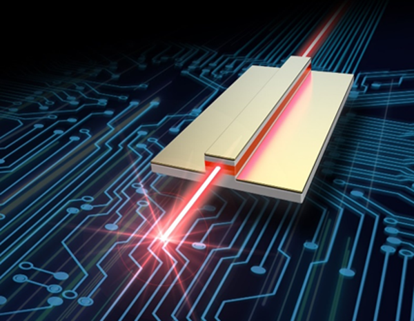
Fig. 1 The GeSn double heterostructure laser is composited by the all-group-IV semiconductor and alloy (namely Si, Ge, GeSn, and SiGeSn), enabling the monolithic integration of lasers on the Si platform.
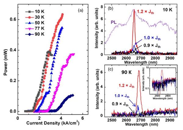
Fig. 2 Characterizations of laser diode with high Sn composition. (a) Temperature-dependent L-I curve. (b) Lasing spectra under injections below and above threshold at 10 K. The PL spectrum was also plotted for comparison. (c) Emission spectra under injections below and above threshold at 90 K; inset: semi-log plot of the spectra.