Journals > > Topics > Nanophotonics
Nanophotonics|7 Article(s)
Rectangular dielectric metagrating for high-efficiency diffraction with large-angle deflection|On the Cover
Weiyi Shi, Weimin Deng, Weinan Liu, Zepeng Zhuang, Zhibin Fan, and Jianwen Dong
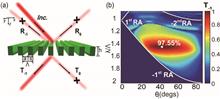
In this Letter, we propose a metagrating consisting of simple rectangular bars for nearly unity anomalous diffraction with a large deflection angle. The analysis performed by the scattering-matrix method shows that such exceptional beam steering derives from the couplings of the two lowest propagation waveguide-array-modes and their constructive interferences. The tolerance of the incident angle for a high diffraction efficiency (e.g., >90%) is within a range of 33°. We also discuss that such an advantage still exists after considering a reasonable loss and dispersion. We envision that the proposed strategy may have wide use in the field of high-performance wavefront-shaping applications. In this Letter, we propose a metagrating consisting of simple rectangular bars for nearly unity anomalous diffraction with a large deflection angle. The analysis performed by the scattering-matrix method shows that such exceptional beam steering derives from the couplings of the two lowest propagation waveguide-array-modes and their constructive interferences. The tolerance of the incident angle for a high diffraction efficiency (e.g., >90%) is within a range of 33°. We also discuss that such an advantage still exists after considering a reasonable loss and dispersion. We envision that the proposed strategy may have wide use in the field of high-performance wavefront-shaping applications.
Chinese Optics Letters
- Publication Date: Jul. 10, 2020
- Vol. 18, Issue 7, 073601 (2020)


High-Q factor photonic crystal cavities with cut air holes [Invited]|Editors' Pick
Liang Fang, Xuetao Gan, and Jianlin Zhao
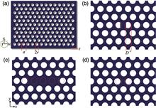
Planar photonic crystal (PPC) cavities with high quality (Q) factors were currently designed by missing or moving air holes. Here, we propose that cutting air holes in PPC into semicircles could be considered as another strategy to realize and optimize cavities, presenting superiorities over cavities with missed or moved air holes in a higher Q factor and a smaller mode volume (Vmode). Examples are demonstrated: (1) in a PPC lattice, cutting two adjacent air holes promises a cavity mode with a Q exceeding 200,500 and an ultrasmall mode volume Vmode λ/2 n)3; (2) in a PPC waveguide, cutting two air holes on opposite sides of the waveguide supports a cavity mode with a Q exceeding 104,600 and a Vmode λ/2 n)3; (3) cutting the two air holes at the edges of an L3-type PPC cavity, the Q factor is optimized from 5500 to 124,700, with an almost constant Vmode. The concept of cutting air holes to introduce defects in PPC also promises the design of PPC also waveguides with an engineered transmission loss and dispersion. Planar photonic crystal (PPC) cavities with high quality (Q) factors were currently designed by missing or moving air holes. Here, we propose that cutting air holes in PPC into semicircles could be considered as another strategy to realize and optimize cavities, presenting superiorities over cavities with missed or moved air holes in a higher Q factor and a smaller mode volume (Vmode). Examples are demonstrated: (1) in a PPC lattice, cutting two adjacent air holes promises a cavity mode with a Q exceeding 200,500 and an ultrasmall mode volume Vmode λ/2 n)3; (2) in a PPC waveguide, cutting two air holes on opposite sides of the waveguide supports a cavity mode with a Q exceeding 104,600 and a Vmode λ/2 n)3; (3) cutting the two air holes at the edges of an L3-type PPC cavity, the Q factor is optimized from 5500 to 124,700, with an almost constant Vmode. The concept of cutting air holes to introduce defects in PPC also promises the design of PPC also waveguides with an engineered transmission loss and dispersion.
Chinese Optics Letters
- Publication Date: Jun. 10, 2020
- Vol. 18, Issue 6, 063603 (2020)
Broadband transverse displacement sensing of silicon hollow nanodisk under focused radial polarization illumination in the near-infrared region
Jianxin Wang, Xianghui Wang, and Ming Zeng
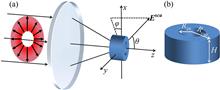
Broadband transverse displacement sensing by exploiting the interaction of a focused radially polarized beam with a silicon hollow nanodisk is proposed. The multipolar decomposition analysis indicates that the interference between a longitudinal total electric dipole (TED) moment and a lateral magnetic dipole (MD) moment is dominant in the far-field transverse scattering in the near-infrared region. Within a broadband wavelength range with the width of 155 nm, the longitudinal TED is almost in phase with the lateral MD, and then broadband position sensing based on the sensitivity of scattering directivity to transverse displacement can be achieved. Broadband transverse displacement sensing by exploiting the interaction of a focused radially polarized beam with a silicon hollow nanodisk is proposed. The multipolar decomposition analysis indicates that the interference between a longitudinal total electric dipole (TED) moment and a lateral magnetic dipole (MD) moment is dominant in the far-field transverse scattering in the near-infrared region. Within a broadband wavelength range with the width of 155 nm, the longitudinal TED is almost in phase with the lateral MD, and then broadband position sensing based on the sensitivity of scattering directivity to transverse displacement can be achieved.
Chinese Optics Letters
- Publication Date: Jun. 10, 2020
- Vol. 18, Issue 6, 063602 (2020)
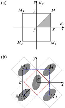
Tunable reducibility of Brillouin zone and bandgap width in elliptical nanowire arrays
Zongyi Zhang, Yonggang Wu, Zihuan Xia, Jian Zhou, and Xuefei Qin
Rotating elliptical nanowire arrays as two-dimensional photonic crystals has been proposed and studied in this Letter. The analysis of the four lowest energy bands and the first bandgap width of some examples illustrates that the rotation and configuration of the primitive cell can have effects on the reducibility of the Brillouin zone. As the central element’s orientation changes, the irreducible Brillouin zone could be expanded to the whole first Brillouin zone. Special attention has been paid to the nanowire arrays with adjacent elements perpendicular to each other, and the irreducible Brillouin zone unexpectedly retracted back to the 1/8 of the first Brillouin zone though the symmetry of elements is lower than that of the square lattice. Meanwhile, the first bandgap width of the perpendicular array can be adjusted by the rotation of each primitive element. Rotating elliptical nanowire arrays as two-dimensional photonic crystals has been proposed and studied in this Letter. The analysis of the four lowest energy bands and the first bandgap width of some examples illustrates that the rotation and configuration of the primitive cell can have effects on the reducibility of the Brillouin zone. As the central element’s orientation changes, the irreducible Brillouin zone could be expanded to the whole first Brillouin zone. Special attention has been paid to the nanowire arrays with adjacent elements perpendicular to each other, and the irreducible Brillouin zone unexpectedly retracted back to the 1/8 of the first Brillouin zone though the symmetry of elements is lower than that of the square lattice. Meanwhile, the first bandgap width of the perpendicular array can be adjusted by the rotation of each primitive element.
Chinese Optics Letters
- Publication Date: Jun. 10, 2020
- Vol. 18, Issue 6, 063601 (2020)
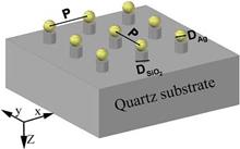
Effects of different structural parameters and the medium environment on plasmonic lattice resonance formed by Ag nanospheres on SiO2 nanopillar arrays
Xiaodan Huang, Chaogang Lou, Hao Zhang, and Hua Yang
The effects of the diameter of SiO2 nanopillars, the diameter of Ag nanospheres, the arrays’ period, and the medium environment on the plasmonic lattice resonance (PLR) formed by Ag nanospheres on SiO2 nanopillar arrays are systematically investigated. Larger diameters of SiO2 nanopillars with other parameters kept constant will widen the PLR peak, redshift the PLR wavelength, and weaken the PLR intensity. Larger diameters of Ag nanospheres with other parameters kept constant will widen the PLR peak, redshift the PLR wavelength, and strengthen the PLR intensity. Larger array periods or larger refractive index of medium environment corresponds to larger PLR wavelengths. The effects of the diameter of SiO2 nanopillars, the diameter of Ag nanospheres, the arrays’ period, and the medium environment on the plasmonic lattice resonance (PLR) formed by Ag nanospheres on SiO2 nanopillar arrays are systematically investigated. Larger diameters of SiO2 nanopillars with other parameters kept constant will widen the PLR peak, redshift the PLR wavelength, and weaken the PLR intensity. Larger diameters of Ag nanospheres with other parameters kept constant will widen the PLR peak, redshift the PLR wavelength, and strengthen the PLR intensity. Larger array periods or larger refractive index of medium environment corresponds to larger PLR wavelengths.
Chinese Optics Letters
- Publication Date: Mar. 10, 2020
- Vol. 18, Issue 3, 033601 (2020)

Ultrafast direct laser writing of 2D materials for multifunctional photonics devices [Invited]|On the Cover
Tieshan Yang, Han Lin, and Baohua Jia
Recently, fundamental properties and practical applications of two-dimensional (2D) materials have attracted tremendous interest. Micro/nanostructures and functional devices in 2D materials have been fabricated by various methods. Ultrafast direct laser writing (DLW) with the advantages of rich light-matter interactions; unique three-dimensional processing capability; arbitrary-shape design flexibility; and minimized thermal effect, which enables high fabrication accuracy resolution, has been widely applied in the fabrication of 2D materials for multifunctional devices. This timely review summarizes the laser interactions with 2D materials and the advances in diverse functional photonics devices by DLW. The perspectives and challenges in designing and improving laser-fabricated 2D material photonic devices are also discussed. Recently, fundamental properties and practical applications of two-dimensional (2D) materials have attracted tremendous interest. Micro/nanostructures and functional devices in 2D materials have been fabricated by various methods. Ultrafast direct laser writing (DLW) with the advantages of rich light-matter interactions; unique three-dimensional processing capability; arbitrary-shape design flexibility; and minimized thermal effect, which enables high fabrication accuracy resolution, has been widely applied in the fabrication of 2D materials for multifunctional devices. This timely review summarizes the laser interactions with 2D materials and the advances in diverse functional photonics devices by DLW. The perspectives and challenges in designing and improving laser-fabricated 2D material photonic devices are also discussed.
Chinese Optics Letters
- Publication Date: Feb. 10, 2020
- Vol. 18, Issue 2, 023601 (2020)
A controllable coupling structure for silicon microring resonators based on adiabatic elimination|On the Cover
Fenghe Yang, Pengfei Sun, Ruixuan Chen, and Zhiping Zhou
Optical microring resonators are extensively employed in a wide range of physical studies and applications due to the resonance enhancement property. Incorporating coupling control of a microring resonator is necessary in many scenarios, but modifications are essentially added to the resonator and impair the capability of optical enhancement. Here, we propose a flexible coupling structure based on adiabatic elimination that allows low-loss active coupling control without any modifications to the resonators. The self-coupling coefficient can be monotonically or non-monotonically controllable by the proposed coupler, potentially at a high speed. The characteristic of the coupler when implemented in silicon microring resonators is investigated in detail using substantiated analytical theory and experiments. This work provides a general method in coupling control while ensuring the resonance enhancement property, making active coupling control in a resonator-waveguide system feasible. Optical microring resonators are extensively employed in a wide range of physical studies and applications due to the resonance enhancement property. Incorporating coupling control of a microring resonator is necessary in many scenarios, but modifications are essentially added to the resonator and impair the capability of optical enhancement. Here, we propose a flexible coupling structure based on adiabatic elimination that allows low-loss active coupling control without any modifications to the resonators. The self-coupling coefficient can be monotonically or non-monotonically controllable by the proposed coupler, potentially at a high speed. The characteristic of the coupler when implemented in silicon microring resonators is investigated in detail using substantiated analytical theory and experiments. This work provides a general method in coupling control while ensuring the resonance enhancement property, making active coupling control in a resonator-waveguide system feasible.
Chinese Optics Letters
- Publication Date: Jan. 10, 2020
- Vol. 18, Issue 1, 013601 (2020)
Topics
© Copyright 2018-2021 | Chinese Laser Press. All Rights Reserved 沪ICP备15018463号-20