
Hao Yang, Jian Cheng, Zhichao Liu, Qi Liu, Linjie Zhao, Chao Tan, Jian Wang, Mingjun Chen. Potential damage threats to downstream optics caused by Gaussian mitigation pits on rear KDP surface[J]. High Power Laser Science and Engineering, 2020, 8(4): 04000e37
- High Power Laser Science and Engineering
- Vol. 8, Issue 4, 04000e37 (2020)
Abstract
1 Introduction
The issue of laser damage to potassium dihydrogen phosphate (KDP) crystal is an important factor restricting the development of high-power laser facilities for inertial confinement fusion (ICF) such as the National Ignition Facility (NIF) in the United States, the Laser MegaJoule in France and the Shenguang Laser Facility in China[
As for the mitigation processes on the surface of KDP crystal, some related research has been explored in the last twenty years[7,11,12]. Hrubesh et al.[10] from the Lawrence Livermore National Laboratory (LLNL) used CW-CO2 laser processing, aqueous wet-etching, short-pulse laser ablation and micromachining to repair laser damage sites on the surface of KDP crystal. The experimental results showed that the micro-milling process proved to be the most effective method for repairing KDP crystals. Next, Geraghty et al.[13] successfully tested all of the shaped contours of mitigation pits on KDP crystal. The laser-induced damage thresholds (LIDTs) were close to the values for the original KDP surface. Elhadj et al.[14] investigated an improved approach for mitigating the damage sites on crystal optic surfaces with the removal of damaged anti-reflective coating. The effect of repaired mitigation shapes on laser damage resistance has been analyzed using a method based on electromagnetic field theory. Using the finite-difference time-domain (FDTD) method, Cheng et al.[15] calculated the light intensification inside KDP crystal with and without mitigation pits, and verified that spherical mitigation pits with a large width–depth ratio can significantly mitigate surface damage growth by lowering the induced light intensification. Finite element method (FEM) models of mitigation pits with various structural parameters were established by Yang et al.[16] to compare the light intensification caused by mitigation pits. It was found that mitigation pits with width–depth ratios greater than 5.3 and 4.3 should be applied in repaired spherical and Gaussian mitigation contours, respectively, to achieve the optimal mitigation effect.
Although the strategy and process for laser damage mitigation on KDP crystal surface have made great progress, the effect of KDP surface mitigation contours upon downstream far-field light modulation is unclear. The downstream light intensity modulation induced by the phase defects that lie on the reflection optics in one of the SG-III laser beamlines was studied by Zhang et al.[17]. They found that these surface phased defects result in strong intensity modulation after some propagation distance. Downstream light-field modulation for mitigated glass has been the subject of research, and it was found that some mitigation structure would be harmful to the downstream optics[18,19]. Fused silica elements are traditionally placed after frequency converters made from KDP materials, which impose a lower relative laser damage threshold at these positions versus other components[5]. Therefore, it is of significance to clarify the influence of KDP mitigation profile on downstream light-field modulation.
Sign up for High Power Laser Science and Engineering TOC. Get the latest issue of High Power Laser Science and Engineering delivered right to you!Sign up now
In order to determine whether mitigation pits on KDP surfaces would reduce the laser damage resistance of downstream optical components, we built a model to calculate downstream light-field modulation caused by mitigation pits on the KDP rear surface based on the angular spectrum diffraction theory. The light-field modulations at different downstream locations caused by Gaussian mitigation pits were then calculated. The micro-milling method is used to replace the damage site on the KDP rear surface by a Gaussian mitigation pit with a width of 800 μm and a depth of 10 μm. The laser damage experiment for downstream optical components is designed to verify the effect of rear-surface Gaussian mitigation pits on the laser damage resistance of downstream far-field optical components. The results are not just used as evidence of the potential damage threats to downstream optics caused by Gaussian mitigation pits on a KDP rear surface, but also provide technical indexes for the installation of downstream optical elements, such as continuous phase plates and wedged focus lenses.
2 Model and theory
Gaussian geometrical contours are generally designed to mitigate the KDP crystal, which alleviates the growth behavior of laser damage sites[15,16]. They can be described by
 (1)
(1)Here, the width and depth of the Gaussian contour are w = 800 μm and d = 10 μm, respectively.
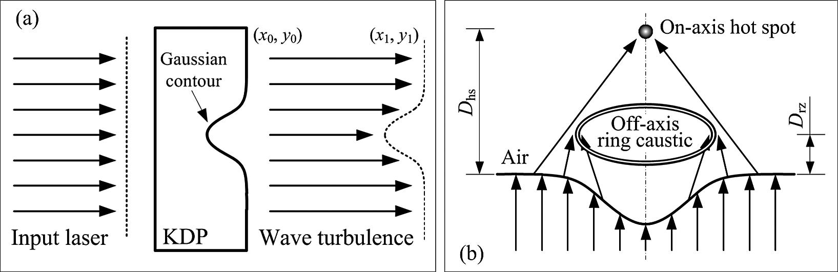
Figure 1.The effect of the Gaussian mitigation pit on the far-field propagation of the outgoing laser. (a) Sketch of the far-field modulation caused by the Gaussian mitigation contour on a KDP rear surface. (b) The relative positions of two dominant downstream light intensification patterns caused by the Gaussian mitigation pit on a KDP rear surface.
The diffraction effect of the downstream light field and the position of the light-intensity enhancement can be preliminarily analyzed by traditional geometric optics theory. Figure 1(b) shows the relative positions of two dominant downstream light intensification patterns caused by the Gaussian mitigation pit on a KDP rear surface. Dhs and Drz refer to the focal lengths of on-axis hot spot and off-axis ring caustic, respectively. The off-axis ring caustic is mainly due to the arc contour around the Gaussian mitigation pit, which produces effects like a convex lens. The position of the on-axis hot spot appears relatively farther than that of the off-axis ring caustic. The hot spot is caused by the diffraction effect of uneven phase distribution of the outgoing light from the KDP rear surface.
The diffraction of the downstream light field behind the mitigation pit on a KDP rear surface can be numerically calculated using scalar diffraction theory. Since the model calculation only focuses on the light-intensity distribution at various locations downstream, the time term in Maxwell’s equations is eliminated. The Helmholtz equation without a time factor can then be obtained as[20]
 (3)
(3)Since the light-intensity distribution of the laser beam is proportional to the square of the amplitude, the product of the complex amplitude and its conjugate complex, as shown in Equation (4), can represent the intensity of the light wave
 (4)
(4)The model introduces the concept of modulation degree M to characterize the degree of disturbance of light-intensity distribution at various downstream positions, as shown in
 (5)
(5)3 Experiment
In order to verify the influence of the KDP rear surface with Gaussian mitigation pits on downstream light-field modulations, three sets of experiments were carried out: fabrication of a Gaussian mitigation pit on a KDP rear surface with the micro-milling method, a test of LIDTs of a downstream fused silica surface and a KDP rear surface with a Gaussian mitigation pit, and a test of downstream laser damage at a fixed distance from the Gaussian mitigation pit on a KDP rear surface.
Gaussian mitigation pits were fabricated by micro-milling on KDP rear surfaces to provide experimental samples for subsequent laser damage experiments. A self-developed multi-axis micro-milling platform was used to mitigate the laser damage point on the rear surface of KDP crystal[16]. A Gaussian mitigation pit of 800 μm width and 10 μm depth is a common set of structure parameters, which could mitigate 60.9% of laser damage sites on the KDP surface. The mitigation pit meets the criterion that the width–depth ratio of the Gaussian contour should be greater than 4.3[16]. In addition, a ball-end cutter with a diameter of 500 μm is used. There is no interference between the Gaussian contour and the cutting tool during machining. The large width–depth ratio and high-quality repaired surface would contribute to improving the laser damage resistance of the KDP crystal. Thus, the rounded Gaussian profile is designed to replace the brittle fracture on the original damage site.
Subsequently, the LIDTs of KDP crystal with Gaussian mitigation pits and finished fused silica were measured. The test was performed on a laser damage test platform for small aperture optical components[16]. The one-on-one test strategy for LIDT was used in the experiment. When plasma flashes in the laser irradiation area near the KDP crystal or fused silica, laser damage is considered to have taken place.
![]()
Figure 2.Laser damage test of a downstream fused silica component induced by a Gaussian mitigation pit on the KDP rear surface. (a) Optical path diagram of the laser damage experiment for downstream fused silica components. (b) Schematic of laser irradiation to a Gaussian mitigation pit on the rear surface of a KDP crystal.
4 Results and discussion
4.1 Downstream light-field perturbation caused by Gaussian mitigation contour
![]()
Figure 3.The far-field diffraction patterns caused by the Gaussian mitigation contour with a width of 800 μm and a depth of 10 μm at downstream distance of (a)
![]()
Figure 4.Comparison of the downstream light-field modulations between the Gaussian mitigation pits on KDP crystal and fused silica.
4.2 Gaussian mitigation pit manufacture
![]()
Figure 5.Microscopic morphology of laser damage and Gaussian mitigation profile. (a) SEM image of a laser damage site on the surface of a KDP crystal. (b) Optical micrograph of a KDP surface with a Gaussian mitigation pit. The inset is the three-dimensional shape of the Gaussian mitigation pit with a width of 800 μm and a depth of 10 μm. (c) Two-dimensional profile of the Gaussian mitigation pit and the damage site. The first inset is the local enhanced image. The second inset shows the edge profile of the mitigated KDP contour and the mitigated fused silica contour.
Figure 5(b) shows an optical micrograph of the KDP surface with a Gaussian mitigation pit after the micro-milling processes. The inset is the three-dimensional shape of the Gaussian mitigation pit with a width of 800 μm and a depth of 10 μm. The material near the surface defects of the KDP crystal is removed and substituted with the designed mitigation contours. The repaired crystal surface is regular, smooth and neat, with a surface roughness better than 30 nm. The relative transmittance of the repaired crystal surface is greater than 95% compared with that of a diamond fly-cut KDP surface. Figure 5(c) is the two-dimensional profile of the Gaussian mitigation pit and the damage site. The damage site on the crystal surface is completely enveloped by the repaired contour. The inset of the local enhanced image shows that even at the waist where the slope changes the most, the repair surface remains smooth. Due to the different processing methods for surface repair on KDP crystal and fused silica, the surrounding raised rim would be produced on the edge contour of the mitigated fused silica surface, which can be seen in the second inset. This rim is formed from the mass movement of silica at high temperatures from the low viscosity central region outwards during CW-CO2 laser processing, and can be several microns high. The micro-mechanical method is utilized to repair the KDP surface, however. The repair process is more controllable and there is no rim similar to the fused silica on the edge of the mitigated KDP contour. Thus, the Gaussian mitigation pit in the model can fully describe the repaired contour.
4.3 Laser-induced damage thresholds
![]()
Figure 6.LIDTs for the Gaussian mitigation pit on (a) the KDP rear surface and (b) the front surface of fused silica.
4.4 Laser damage performance of downstream fused silica components
![]()
Figure 7.Comparison of the downstream light-field modulations caused by a Gaussian mitigation pit on the KDP rear surface with irradiation by flat-top laser and Gaussian laser. (a) Simulation schematic of light propagation when the KDP rear surface with mitigation pit is irradiated by incident laser. (b) Comparison of the light-field modulation generated by the flat-top laser and the Gaussian laser at a position 10 mm downstream. The inset is a diffraction pattern produced by a Gaussian laser at a position 10 mm downstream away from the crystal surface with a mitigation pit when the center point distance
![]()
Figure 8.Microscopic morphology of the laser damage sites on downstream fused silica surface observed by SEM. (a) Pansy damage site; (b) mussel damage sites.
![]()
Figure 9.Comparison between the calculations and experiments. (a) Two-dimensional distribution of downstream light-field modulation along the laser propagation (
5 Conclusions
The effects of Gaussian mitigation pits on the rear surfaces of KDP crystals upon the laser damage property of downstream fused silica optics were theoretically and experimentally investigated. By calculating the downstream light-intensity distribution from the KDP rear surface with mitigation pits of various widths and depths, it is found that severe light intensification is produced in the downstream light field due to the phase contrast and its induced diffraction effect. The downstream light-field modulations induced by Gaussian mitigation pits would change with various downstream locations, and two modulation curve peaks are generated due to the off-axis ring caustic and the on-axis hot spot. The main peak near the rear surface of the crystal is modulated more heavily, posing a bigger threat to downstream fused silica optics. Different from the mitigation effect of the fused silica, there is a lesser secondary peak caused by the Gaussian mitigation pits on the KDP crystal. The experimental results for laser damage upon downstream fused silica show that the Gaussian mitigation pit on the rear surface of the crystal would cause LID on downstream fused silica at a position 10 mm away from the KDP rear surface. The location and probability of the laser damage sites are consistent with the simulations, which proves that the theoretical results of downstream light-field modulation calculated by angular spectrum diffraction theory are valid and effective. This work could provide theoretical and experimental guidance for the subsequent repair processes and installation of KDP crystal components.
References
[1] R. A. Hawley-Fedder, P. Geraghty, S. N. Locke. Proc. SPIE, 5341, 121.
[2] E. I. Moses. Fusion Eng. Des., 85, 983(2010).
[3] D. Besnard. Eur. Phys. J. D, 44, 207(2006).
[4] J. J. De Yoreo, A. K. Burnham, P. K. Whitman. Int. Mater. Rev., 47, 113(2002).
[5] K. R. Manes, M. L. Spaeth, J. J. Adams. Fusion Sci. Technol., 69, 146(2016).
[6] D. Chen, B. Wang, H. Wang. High Power Laser Sci. Eng., 8, e6(2020).
[7] M. L. Spaeth, P. J. Wegner, T. I. Suratwala. Fusion Sci. Technol., 69, 265(2016).
[8] S. G. Demos, M. R. Kozlowski, M. Staggs, L. L. Chase, A. Bumham, H. B. Radousky. Proc. SPIE, 4347, 277(2001).
[9] X. Chu, H. Zhang, Z. Tian. High Power Laser Sci. Eng., 7, e66(2019).
[10] L. W. Hrubesh, R. B. Brusasco, W. Grundler. Proc. SPIE, 4923, 180(2002).
[11] W. Gao, J. Ji, C. Wang. Opt. Mater. Express, 8, 2625(2018).
[12] M. Chen, N. Chen, N. He, H. Ni, Z. Liu, L. Li. J. Mech. Eng., 50, 161(2014).
[13] P. Geraghty, W. Carr, V. raggoo, R. Hackel, C. Mailhiot, M. Norton. Proc. SPIE, 6403, 64030Q(2006).
[14] S. Elhadj, W. A. Steele, D. S. Vanblarcom, R. A. Hawley, K. I. Schaffers, P. Geraghty. Appl. Opt., 56, 2217(2017).
[15] J. Cheng, M. Chen, W. Liao, H. Wang, Y. Xiao, M. Li. Opt. Express, 21(2013).
[16] H. Yang, J. Cheng, M. Chen. Opt. Express, 25(2017).
[17] X. Zhang, W. Zhou, W. Dai. High Power Laser Sci. Eng., 4, e6(2016).
[18] T. Doualle, L. Gallais, S. Monneret. Proc. SPIE, 10014(2016).
[19] Y. Jiang, Q. Zhou, R. Qi. Chin. Phys. B, 25(2016).
[20] A. Bourgeade, T. Donval, L. Gallais, L. Lamaignère, J. L. Rullier. J. Opt. Soc. Am. B, 32, 655(2015).
[21] Y. Bai, L. Zhang, W. Liao. Acta. Phys. Sin., 65(2016).
[22] C. W. Carr, M. J. Matthews, J. D. Bude, M. L. Spaeth. Proc. SPIE, 6403(2006).
[23] C. W. Carr, D. A. Cross, M. A. Norton, R. A. Negres. Opt. Express, 19(2011).
[24] J. Wong, J. L. Ferriera, E. F. Lindsey, D. L. Haupt, I. D. Hutcheon, J. H. Kinney. J. Non-Cryst. Solids, 352, 255(2006).

Set citation alerts for the article
Please enter your email address
© Copyright 2018-2021 | Chinese Laser Press. All Rights Reserved 沪ICP备15018463号-20