• Advanced Photonics
  • Vol. 4, Issue 4, 046004 (2022)
Zhixia Xu1、2、†, Jie Chang2, Jinye Tong2, Daniel F. Sievenpiper3、*, and Tie Jun Cui1、*
Author Affiliations
  • 1Southeast University, State Key Laboratory of Millimeter Waves, Nanjing, China
  • 2Dalian Maritime University, School of Information Science and Technology, Dalian, China
  • 3University of California San Diego, Department of Electrical and Computer Engineering, San Diego, California, United States
  • show less
    DOI: 10.1117/1.AP.4.4.046004 Cite this Article Set citation alerts
    Zhixia Xu, Jie Chang, Jinye Tong, Daniel F. Sievenpiper, Tie Jun Cui. Near-field chiral excitation of universal spin-momentum locking transport of edge waves in microwave metamaterials[J]. Advanced Photonics, 2022, 4(4): 046004 Copy Citation Text show less
    Spin-momentum locking exists at the interface of two metamaterials. (a) The chirality of the source decides the transmission direction. Unidirectional transmission at the interface between: (b) spoof SPPs: air and corrugated structures (εair>0, εeff<0); (c) LWs: dual-impedance surfaces (ZTM>0, ZTE<0); and (d) PTIs: Berry phase flips.
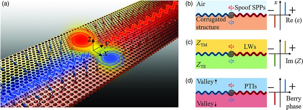
    Fig. 1. Spin-momentum locking exists at the interface of two metamaterials. (a) The chirality of the source decides the transmission direction. Unidirectional transmission at the interface between: (b) spoof SPPs: air and corrugated structures (εair>0, εeff<0); (c) LWs: dual-impedance surfaces (ZTM>0, ZTE<0); and (d) PTIs: Berry phase flips.
    Two chiral sources carrying (a) SAM and (b) OAM. (c) Spin-momentum locking phenomenon. (d) SAM-OAM conversion. (e) Five-ports-feeding network and measured performance: (f) balanced amplitude and (g) π/2-phase step.
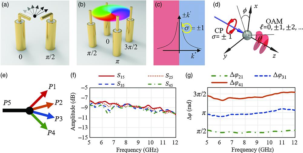
    Fig. 2. Two chiral sources carrying (a) SAM and (b) OAM. (c) Spin-momentum locking phenomenon. (d) SAM-OAM conversion. (e) Five-ports-feeding network and measured performance: (f) balanced amplitude and (g) π/2-phase step.
    (a) Spoof SPPs under study. (b) Enlarged absorptive terminal design. (c) Electric field vector of spoof SPPs with spin-momentum locking. (d) Dispersion curves of two spoof SPPs (SSPPs).
    Fig. 3. (a) Spoof SPPs under study. (b) Enlarged absorptive terminal design. (c) Electric field vector of spoof SPPs with spin-momentum locking. (d) Dispersion curves of two spoof SPPs (SSPPs).
    Visualization of unidirectional spoof SPPs. (a) The near-field scanning setup. (b) Transmission at two opposite terminals excited by an RHCP source. (c) Measured distribution of the out-of-plane electric field (Ez) at 10 GHz along the transmission route. (d) Field distributions on the 2D surface. (e) The planar structure is wrapped on the surface of a cylinder. (f) Unidirectional coupling on the surface of the cylinder [unidirectional planar spoof SPPs (Video 1, MP4, 2.26 MB [URL: https://doi.org/10.1117/1.AP.4.4.046004.1]) and unidirectional conformal spoof SPPs (Video 2, MP4, 1.59 MB [URL: https://doi.org/10.1117/1.AP.4.4.046004.2)].
    Fig. 4. Visualization of unidirectional spoof SPPs. (a) The near-field scanning setup. (b) Transmission at two opposite terminals excited by an RHCP source. (c) Measured distribution of the out-of-plane electric field (Ez) at 10 GHz along the transmission route. (d) Field distributions on the 2D surface. (e) The planar structure is wrapped on the surface of a cylinder. (f) Unidirectional coupling on the surface of the cylinder [unidirectional planar spoof SPPs (Video 1, MP4, 2.26 MB [URL: https://doi.org/10.1117/1.AP.4.4.046004.1]) and unidirectional conformal spoof SPPs (Video 2, MP4, 1.59 MB [URL: https://doi.org/10.1117/1.AP.4.4.046004.2)].
    (a) Structure of the LWs waveguide under study. (b) Electric field distribution at the x-z cross section. (c) Dispersion curves of surface modes and LWs, and equivalent surface reactance can be calculated. Black solid line: dispersion curves of surface waves and LWs. Gray dashed line: light cone. Colored dashed line: extracted surface impedance.
    Fig. 5. (a) Structure of the LWs waveguide under study. (b) Electric field distribution at the x-z cross section. (c) Dispersion curves of surface modes and LWs, and equivalent surface reactance can be calculated. Black solid line: dispersion curves of surface waves and LWs. Gray dashed line: light cone. Colored dashed line: extracted surface impedance.
    Visualization of unidirectional LWs. (a) The near-field scanning setup. (b) Simulated electric field (Ez) distribution on the surface of the planar structure where we set up uniform equivalent impedance surfaces as a simplified simulation model. (c) Measured electric field (Ez) distribution [unidirectional LWs (Video 3, MP4, 2.99 MB [URL: https://doi.org/10.1117/1.AP.4.4.046004.3])].
    Fig. 6. Visualization of unidirectional LWs. (a) The near-field scanning setup. (b) Simulated electric field (Ez) distribution on the surface of the planar structure where we set up uniform equivalent impedance surfaces as a simplified simulation model. (c) Measured electric field (Ez) distribution [unidirectional LWs (Video 3, MP4, 2.99 MB [URL: https://doi.org/10.1117/1.AP.4.4.046004.3])].
    (a) The valley waveguide. (b) Unit cell analysis: topological bandgap, intrinsic OAM (l=±1), and flipping Berry curvature. (c) Superlattice analysis: dispersion and field distributions of valley PTIs at two different interfaces. Unidirectional OAM coupling with (d) different vortex charges l and (e) different phase step Δφ. The transmission is defined by the proportion of received energy at terminals (left/right) and the total energy of the source: T=Pleft/right/Psource. The maximum transmission (T=1) represents an ideal unidirectional coupling.
    Fig. 7. (a) The valley waveguide. (b) Unit cell analysis: topological bandgap, intrinsic OAM (l=±1), and flipping Berry curvature. (c) Superlattice analysis: dispersion and field distributions of valley PTIs at two different interfaces. Unidirectional OAM coupling with (d) different vortex charges l and (e) different phase step Δφ. The transmission is defined by the proportion of received energy at terminals (left/right) and the total energy of the source: T=Pleft/right/Psource. The maximum transmission (T=1) represents an ideal unidirectional coupling.
    Visualization of unidirectional valley PTIs. (a) Near-field scanning setup. (b) Simulated electric field distributions of two waveguides with horn-type and straight-line-type terminals. (c) Measured electric field distribution at opposite terminals. (d) Measured unidirectional transmission [unidirectional valley PTIs with the horn-type terminal (Video 4, MP4, 1.32 MB [URL: https://doi.org/10.1117/1.AP.4.4.046004.4]) and unidirectional valley PTIs with the straight-line-type terminal (Video 5, MP4, 1.26 MB [URL: https://doi.org/10.1117/1.AP.4.4.046004.5])].
    Fig. 8. Visualization of unidirectional valley PTIs. (a) Near-field scanning setup. (b) Simulated electric field distributions of two waveguides with horn-type and straight-line-type terminals. (c) Measured electric field distribution at opposite terminals. (d) Measured unidirectional transmission [unidirectional valley PTIs with the horn-type terminal (Video 4, MP4, 1.32 MB [URL: https://doi.org/10.1117/1.AP.4.4.046004.4]) and unidirectional valley PTIs with the straight-line-type terminal (Video 5, MP4, 1.26 MB [URL: https://doi.org/10.1117/1.AP.4.4.046004.5])].
    Digital coding metamaterial waveguides with spin-momentum locking. (a) Spoof SPPs: manipulating the wavevector and bi-directional chiral sorting. (b) LWs: manipulating impedance to tailor the arbitrary transmission and control the scattering performance of metasurfaces at the same time. (c) PTIs: manipulating the topological invariant to realize dynamic chiral sorting multiplexers.
    Fig. 9. Digital coding metamaterial waveguides with spin-momentum locking. (a) Spoof SPPs: manipulating the wavevector and bi-directional chiral sorting. (b) LWs: manipulating impedance to tailor the arbitrary transmission and control the scattering performance of metasurfaces at the same time. (c) PTIs: manipulating the topological invariant to realize dynamic chiral sorting multiplexers.
    Metamaterial waveguidesChiral sortingWorking bandwidthWave velocityTransmission robustnessPotential applicationsDevice-assisted
    Spoof SPPsSAM/OAMBroadbandSlowFlexibilityWearable, compact circuitsVigorous
    LWsSAM/OAMBroadbandSlowFlexibilityMultifunctional metasurfacesUnexplored
    PTIsSAM/OAMNarrowSlow/fastImmunityIsolators and cavitiesEarly stage
    Table 1. Characteristics of Three Waveguides in the Microwave Band
    Zhixia Xu, Jie Chang, Jinye Tong, Daniel F. Sievenpiper, Tie Jun Cui. Near-field chiral excitation of universal spin-momentum locking transport of edge waves in microwave metamaterials[J]. Advanced Photonics, 2022, 4(4): 046004
    Download Citation