
Lin Chen, Jianhua Zhao, Dieter Weiss, Christian H. Back, Fumihiro Matsukura, Hideo Ohno. Magnetization dynamics and related phenomena in semiconductors with ferromagnetism[J]. Journal of Semiconductors, 2019, 40(8): 081502
- Journal of Semiconductors
- Vol. 40, Issue 8, 081502 (2019)
Abstract
1. Introduction
The ferromagnetic semiconductor (Ga,Mn)As has been utilized to demonstrate proof-of-concept devices since its first synthesis in 1996[
2. Properties of (Ga,Mn)As
Because the thermal-equilibrium solubility of Mn in GaAs is small, non-equilibrium growth method, i.e., low-temperature molecular-beam epitaxy at substrate temperature ~ 250 °C, is developed to synthesize single crystalline (Ga,Mn)As films with on the order of percent of nominal Mn composition x. Its p-type conductivity indicates that most of the Mn atoms (MnGa) act as acceptors by replacing Ga atoms in divalent states (d5 configuration with localized spin of 5/2)[
The itinerant holes, which reside in the valence band of GaAs, mediate Ruderman-Kittel-Kasuya-Yosida (RKKY)-type exchange interaction among Mn spins[
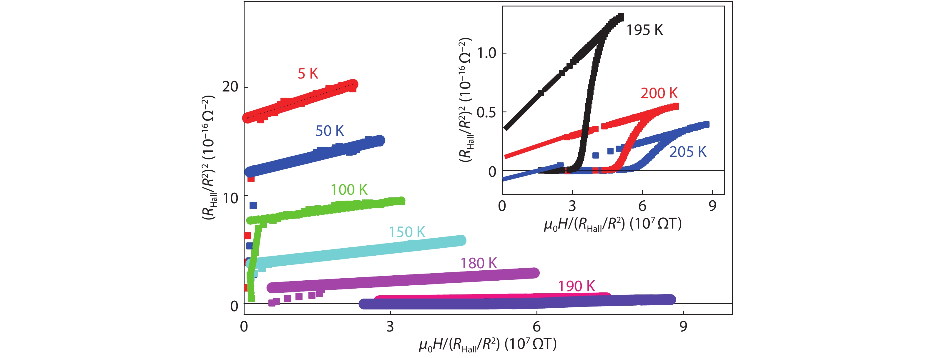
2.1. Curie temperature
In (Ga,Mn)As, the exchange interaction among As 4p and Mn 3d electrons (p–d exchange interaction) results in the ferromagnetic state. According to the p–d Zener model, the Curie temperature TC is proportional to the effective Mn composition participating in the ferromagnetic order, and the density of state at the Fermi level. Therefore, TC increases as the hole concentration p increases by decreasing the number of MnI through annealing. The enhancement of the annealing effect is expected for a (Ga,Mn)As nanowire because of its larger ratio of the surface region than films[
![]()
Figure 1.(Colour online) Arrott plots at different temperatures for a 300 nm-wide Hall bar of (Ga,Mn)As. The inset shows a close-up view of the Arrott plots near the ferromagnetic transition, which confirms that
2.2. Magnetic anisotropy and anisotropic magnetoresistance effect
(Ga,Mn)As shows sizable magnetic anisotropy depending on the spontaneous magnetization M, p, and lattice strain. For example, a metallic (Ga,Mn)As film with compressive strain on a GaAs (001) substrate exhibits an in-plane easy axis for the magnetization, while that with tensile strain on an (In,Ga)As buffer layer shows perpendicular easy axis[
2.3. Carrier localization
Magneto-transport measurements show that (Ga,Mn)As is in the vicinity of the metal-insulator transition (MIT)[
2.4. Electric-field effects
By making a capacitor structure with one of the two electrodes as a thin (Ga,Mn)As film, one can apply an electric-field onto (Ga,Mn)As to change p and the degree of MIT, which in turn alters the magnetic properties of (Ga,Mn)As due to carrier induced ferromagnetism. So far, the electric-field modulation of TC[
3. Ferromagnetic resonance (FMR) and related phenomena in (Ga,Mn)As-based structures
There is an excellent review on the magnetization precession in (Ga,Mn)As induced by optical means[
FMR spectrum is usually measured as the derivative of the microwave absorption, which is well fitted by the derivative of the Lorentz function, − (16I/π){ΔH(H− HR)/[4(H− HR)2+ ΔH2]2}, similar to other conventional ferromagnets. From the fitting, one can determine the absorption coefficient I, resonance field HR, and the linewidth (the full width at half maximum) ΔH. The magnetization dynamics is known to be described by the Landau-Lifshitz-Gilbert (LLG) equation[
and this is also the case for (Ga,Mn)As. Here,
as
with ω = 2πf. From the fitting of Eq. (3) to the magnetic-field angle dependence of HR, one can determine the values of g and magnetic anisotropy fields.
The linewidth induced by intrinsic damping is expressed as[
Extrinsic contributions such as the dispersion of the magnetic anisotropies and roughness as well as two-magnon scattering can also be included phenomenologically in the analysis of the magnetic-field angle θH (or φH) dependence of ΔH to determine the magnitude of α[
3.1. Electric-field effects on FMR spectra
The FMR measurements can be used to determine the magnitude of magnetic anisotropy fields, α, and g. By measuring the FMR spectra under electric-fields, one can determine the electric-field dependence of these parameters. The electric-field effects on the FMR spectra were investigated for a 4-nm thick (Ga,Mn)As film with x = 0.13 annealed at 200 °C for 10 min in a capacitor structure[
Figs. 2(a) and 2(b) show the VG dependence of anisotropic fields Hani and damping constant. The modulation of the magnetic anisotropy fields and g, whose values are expected to be determined by the spin-orbit interaction, is relatively small (~1%). On the other hand, α becomes larger by decreasing p through an electric field, and its modulation reaches ~12%, suggesting that the modulation is not determined only by the spin-orbit interaction. We measure the electrical resistance and magnetization under electric fields and those of some other samples with different conductivities in addition to α. As shown in Fig. 2(c), there is a clear correlation between the resistance, the portion of a superparamagnetic-like component, and α, i.e., a larger portion of the superparamagnetic-like component and larger α for samples with higher resistance. This observation suggests strongly that α in (Ga,Mn)As is determined mainly by the magnetic disorder induced by carrier localization.
![]()
Figure 2.(Colour online) Gate-voltage dependence of (a) magnetic anisotropy fields
The electric-field effect on α was also observed in a thin CoFeB/MgO structure[
3.2. Electrical detection of FMR
In conductive ferromagnets, the relationship between electric field
where ρ is the resistivity,
We prepared a 20-nm thick (Ga,Mn)As film with x = 0.065 on a semi-insulating GaAs (001) substrate, and annealed it at 250 °C for 30 min. TC of the (Ga,Mn)As was 118 K. We measured FMR spectra and DC voltages V along the [110] orientation simultaneously by sweeping H orthogonal to the [110] orientation at f = 9 GHz and at 45 K[
![]()
Figure 3.(Colour online) (a) Ferromagnetic resonance and (b) DC voltage
It was also shown that electrical detection of FMR is possible in (Ga,Mn)As through electric-field excitation[
3.3. Spin pumping and inverse spin Hall effect
Similar to metallic systems[
The measurements of the inverse spin Hall effect was done on virtually identical (Ga,Mn)As films as described in the previous section on a 20-nm thick p-GaAs layer with p = 9.5 × 1018 cm–3 grown on a semi-insulating GaAs substrate[
![]()
Figure 4.(Colour online) The magnetic-field angle
The DC voltage induced by inverse spin Hall effect VISHE is proportional to the damping term in Eq. (1), which can be derived as VISHE ~ Re(mx)Im(my) − Im(mx)Re(my). The lineshape of VISHE is symmetric, which is the same as the planar Hall effect. Note that, being different from VPHE, VISHE results from the combination of the real and imaginary part of the dynamic magnetization. Thus, the separation of the signals induced by the two effects is possible by utilizing the different magnetic-field angle θH dependence of the two signals as shown in Fig. 5. The fitting reproduces well the experimental observation, and indicates contributions of 12% from the inverse spin Hall effect and 88% from the planar Hall effect to symmetric DC voltage[
![]()
Figure 5.(Colour online) Angular dependence of the DC voltage for (Ga,Mn)As/p-GaAs.Magnetic field angle
4. Spin-orbit torques in single crystalline Fe/GaAs (001) hybrid structures
Due to the crystal and structural symmetry breaking in a strained (Ga,Mn)As film, one can induce the effective spin-orbit magnetic field in (Ga,Mn)As by applying electric current, which was utilized to manipulate the magnetization direction and to excite FMR[
where kx (ky) is a [100] ([010]) component of the wavevector
4.1. Quantifying the interfacial spin-orbit field at the Fe/GaAs interface
The strength of the interfacial spin-orbit fields at the Fe/GaAs interface can be quantified using spin-orbit-torque FMR (SO-FMR). The applied RF current to Fe/GaAs produces RF spin-orbit fields, which induce magnetization precession when the resonance condition is fulfilled. The precession results in the periodic change in resistance with precessional frequency through the magnetogalvanic effect in Fe, and thus produces DC voltage V (Eq. (5))[
The sample used for SO-FMR measurements is a 5-nm thick single crystalline Fe grown by MBE on undoped GaAs (001). The Fe layer was patterned into stripes (6.4 × 100 μm2) along different crystal orientations of GaAs, i,e., [100], [010], [110], and
![]()
Figure 6.(Colour online) Experimentally determined magnitude and direction of the in-plane spin-orbit fields, which are normalized by a unit current density of 1011 A/m2.
The spin galvanic effect induced by spin pumping at Fe/GaAs spin-orbit interface was also demonstrated by exciting FMR using an out-of-plane component of an Oersted field in a coplanar waveguide (putting Fe wires a gap between the signal and ground lines of a coplanar waveguide)[
4.2. Electric-field control of interfacial spin-orbit fields
The magnitude of β and α at the Fe/GaAs interface depends linearly on the interfacial electric-field. Thus, it is possible to control the effective spin-orbit field by an external electric-field[
![]()
Figure 7.(Colour online) Polar plot of in-plane spin-orbit fields under different gate-voltages. The arrows represent direction and relative strength of
The electric-field modulation of the interfacial spin-orbit effects is attracting much attention also from the view point of practical applications. For instance, the electric-field induced precessional magnetization switching through the modulation of the interfacial magnetic anisotropy was demonstrated, and this switching scheme is fast with low-power consumption[
4.3. Emergence of anisotropic Gilbert damping at Fe/GaAs interface
The interplay of Bychkov-Rashba and Dresselhaus spin-orbit interaction can modify the density of states at the Fe/GaAs interface. This has caused a rich variety of interfacial spin-orbit related phenomena. It has been found that the symmetry of the anisotropic magneto-resistance[
Fig. 8(a) shows the angular dependence of Gilbert damping for Fe thickness of 1.9 nm determined by analyzing the in-plane magnetic angle φH dependence and the microwave frequency f dependence of the linewidth. Isotropic behavior is observed for 1.9 nm Fe on GaAs. However, clear anisotropic Gilbert damping has been found when the Fe thickness is reduced to 1.3 nm as shown in Fig. 8(b). The anisotropic damping shows two-fold symmetry, coinciding with the symmetry observed for tunneling anisotropic magnetoresistance[
![]()
Figure 8.(Colour online) Magnetic-field angle
5. Conclusion
We have described the fundamental properties of (Ga,Mn)As focusing on its ferromagnetic-resonance (FMR) related phenomena such as the spin pumping and the electric-field modulation of the damping constant. We have described also recent topics on FMR-related phenomena in single crystalline Fe/GaAs structures such as the electric-field modulation of the interfacial spin-orbit fields and the emergence of the anisotropic damping in the structures with an ultrathin Fe. In both systems, (Ga,Mn)As and Fe/GaAs, the observation of the magnetization dynamics provides us the opportunities to investigate a variety of physics based on their spin-orbit interaction.
Acknowledgements
The authors thank T. Dietl, J. Fabian, M. Gmitra, S. Mankovsky, H. Ebert, M. Kronseder, D. Schuh, D. Bougeard for fruitful discussions. L. C. thanks the German Science Foundation (DFG) via SFB 1277 for support. The work at Tohoku University was partially supported by Grant-in-Aids from MEXT and JSPS.
References
[1] H Ohno, A Shen, F Matsukura et al. (Ga,Mn)As: A new diluted magnetic semiconductor based on GaAs. Appl Phys Lett, 69, 363(1996).
[2] T Dietl, H Ohno, F Matsukura et al. Zener model description in ferromagnetism in zinc-blende magnetic semiconductors. Sience, 287, 1019(2000).
[3] T Diet, H Ohno, F Matsukura. Hole-mediated ferromagnetism in tetrahedrally coordinated semiconductors. Phys Rev B, 63, 195205(2001).
[4]
[5] T Dietl, H Ohno. Dilute ferromagnetic semiconductors: Physics and spintronic structures. Rev Mod Phys, 86, 187(2014).
[6] T Jungwirth, J Wunderlich et al. Spin-dependent phenomena and device concepts explored in (Ga,Mn)As. Rev Mod Phys, 86, 855(2014).
[7] J Schneider, W Kaufmann et al. Electronic structure of neutral manganese acceptor in gallium arsenide. Phys Rev Lett, 59, 240(1987).
[8] J Szczytko, J Teardowski, K Świątek et al. Mn impurity in Ga1–
[9] K M Yu, W Walukiewicz, T Wojtowicz et al. Effect of the location of Mn sites in ferromagnetic Ga1–
[10] J Blinowski, P Kacman. Spin interactions of interstitial Mn ions in ferromagnetic GaMnAs. Phys Rev B, 67, 121204(R)(2003).
[11] T Wojtowicz, J K Furdyna, X Liu et al. Electronic effects determining the formation of ferromagnetic III1–
[12] K W Edmonds, P Bogusławski, K Y Wang et al. Mn interstitial diffusion in (Ga,Mn)As. Phys Rev Lett, 92, 037201(2004).
[13] S Souma, L Chen, R Oszwałdowski. Fermi level position, Coulomb gap, and Dresselhaus splitting in (Ga,Mn)As. Sci Rep, 6, 27266(2016).
[14] K F Fid, B L Sheu, O Maksimov et al. Nanoengineered Curie temperature in laterally patterned ferromagnetic semiconductor heterostructures. Appl Phys Lett, 86, 152505(2005).
[15] L Chen, X Yan, F Yang et al. Enhancing the Curie temperature of ferromagnetic semiconductor (Ga,Mn)As to 200 K via nanostructure engineering. Nano Lett, 11, 2584(2011).
[16] A Shen, H Ohno, F Matsukura et al. Epitaxy of (Ga,Mn)As, a new diluted magnetic semiconductor based on GaAs. J Cryst Growth, 175/176, 1069(1997).
[17] T Jungwirth, Q Niu, A H MacDonald. Anomalous Hall effect in ferromagnetic semiconductors. Phys Rev Lett, 88, 207208(2002).
[18] D V Baxter, D Ruzmetov, J Scherschligt et al. Anisotropic magnetoresistance in Ga1–
[19] H X Tang, R K Kawakami, D D Awschalom et al. Giant planar Hall effect in epitaxial (Ga,Mn)As devices. Phys Rev Lett, 90, 107201(2003).
[20] K Pappert, S Hümpfner, J Wenisch et al. Transport characterization of the magnetic anisotropy of (Ga,Mn)As. Appl Phys Lett, 90, 062109(2007).
[21] T Yamada, D Chiba, F Matsukura et al. Magnetic anisotropy in (Ga,Mn)As probed by magnetotransport measurements. Phys Status Solidi C, 3, 4086(2006).
[22] M Abolfath, T Jungwirth, J Brum et al. Theory of magnetic anisotropy in III1–
[23] M Birowska, C Śliwa, J A Majewski et al. Origin of bulk uniaxial anisotropy in zinc-blende dilute magnetic semiconductors. Phys Rev Lett, 108, 237203(2012).
[24] J Zemen, J Kučera, K Olejník et al. Magnetocrystalline anisotropies in (Ga,Mn)As: Systematic theoretical study and comparison with experiment. Phys Rev B, 80, 155203(2009).
[25] W Stefanowicz, C Śliwa, P Alekshkevych et al. Magnetic anisotropy of epitaxial (Ga,Mn)As on (113)A GaAs. Phys Rev B, 81, 155203(2010).
[26] M Sawicki, O Poselkov, C Sliwa et al. Cubic anisotropy in (Ga,Mn)As layers: Experiment and theory. Phys Rev B, 97, 184403(2018).
[27] A Oiwa, S Katsumoto, A Endo et al. Nonmetal-metal-nonmetal transition and large negative magnetoresistance in (Ga,Mn)As/GaAs. Solid State Commun, 103, 209(1997).
[28] T Dietl. Interplay between carrier localization and magnetism in diluted magnetic and ferromagnetic semiconductors. J Phys Soc Jpn, 77, 031005(2008).
[29] M Sawicki, D Chiba, A Korbecka. Experimental probing of the interplay between ferromagnetism and localization in (Ga,Mn)As. Nat Phys, 6, 22(2009).
[30] L Chen, F Matsukura. Electric-field modulation of damping constant in a ferromagnetic semiconductor (Ga,Mn)As. Phys Rev Lett, 115, 057204(2015).
[31] D Chiba, F Matsukura, H Ohno. Electric-field control of ferromagnetism in (Ga,Mn)As. Appl Phys Lett, 89, 162505(2006).
[32] D Chiba, M Sawicki, Y Nishitani et al. Magnetization vector manipulation by electric fields. Nature, 455, 515(2008).
[33] D Chiba, M Werpachowska et al. Anomalous Hall effect in field-effect structures of (Ga,Mn)As. Phys Rev Lett, 104, 106601(2010).
[34] F Matsukura, Y Tokura, H. Ohno. Control of magnetism by electric fields. Nat Nanotechnol, 10, 209(2015).
[35] X Liu, J K Furdyna. Ferromagnetic resonance in Ga1–
[36] T L Gilbert. A phenomenological theory of damping in ferromagnetic materials. IEEE Trans Magn, 40, 3443(2004).
[37] L Chen, F Matsukura, H Ohno. Direct-current voltages in (Ga,Mn)As structures induced by ferromagnetic resonance. Nat Commun, 4, 2055(2013).
[38] H Suhl. Ferromagnetic resonance in nickel ferrite between one and two kilomegacycles. Phys Rev, 97, 555(1955).
[39] S Mizukami, Y Ando. The study on ferromagnetic resonance linewidth for NM/80NiFe/NM (NM = Cu, Ta, Pd and Pt) films. Jpn J Appl Phys, 40, 580(2001).
[40] R Arias, D L Mills. Extrinsic contributions to the ferromagnetic resonance response of ultrathin films. Phys Rev B, 60, 7395(1999).
[41] J Lindner, C Barsukov et al. Two-magnon damping in thin films in case of canted magnetization: Theory versus experiment. Phys Rev B, 80, 224421(2009).
[42] A Okada, S Kanai, M Yamanouchi et al. Electric-field effects on magnetic anisotropy and damping constant in Ta/CoFeB/MgO investigated by ferromagnetic resonance. Appl Phys Lett, 105, 052415(2014).
[43] H J Juretschke. Electromagnetic theory of dc effects in ferromagnetic resonance. J Appl Phys, 31, 1401(1960).
[44] D Fang, H Kurebayashi, J Wunderlich et al. Spin-orbit-driven ferromagnetic resonance. Nat Nanotechnol, 6, 413(2011).
[45] S Mizukami, Y Ando, T Miyazaki. Effect of spin diffusion on Gilbert damping for a very thin permalloy layer in Cu/permalloy/ Cu/Pt films. Phys Rev B, 66, 104413(2002).
[46] Y Tserkovnyak, A Brataas, G E W Bauer. Enhanced Gilbert damping in thin ferromagnetic films. Phys Rev Lett, 88, 117601(2002).
[47] E Saitoh, M Ueda et al. Conversion of spin current into charge current at room temperature: Inverse spin-Hall effect. Appl Phys Lett, 88, 182509(2006).
[48] L Chen, S Ikeda, F Matsukura et al. DC voltages in Py and Py/Pt under ferromagnetic resonance. Appl Phys Express, 7, 013002(2014).
[49] H Nakayama, L Chen, H W Chang et al. Inverse spin Hall effect in Pt/(Ga,Mn)As. Appl Phys Lett, 106, 222405(2015).
[50] S Isogami, M Tsunoda. Enhanced inverse spin-Hall voltage in (001) oriented Fe4N/Pt polycrystalline films without contribution of planar-Hall effect. Jpn J Appl Phys, 55, 043001(2016).
[51] A Chernyshov, M Overby, X Liu et al. Evidence for reversible control of magnetization in a ferromagnetic material by means of spin-orbit magnetic field. Nat Phys, 5, 656(2009).
[52] M Endo, F Matsukura, H Ohno. Current induced effective magnetic field and magnetization reversal in uniaxial anisotropy (Ga,Mn)As. Appl Phys Lett, 97, 222501(2010).
[53] J Moser, A Matos-Abiague, D Schuh et al. Tunneling anisotropic magnetoresistance and spin-orbit coupling in Fe/GaAs/Au tunnel junctions. Phys Rev Lett, 99, 056601(2007).
[54] M Gmitra, A Matos-Abiague, C Draxl et al. Magnetic control of spin-orbit fields: A first-principles study of Fe/GaAs junctions. Phys Rev Lett, 111, 036603(2013).
[55] I Žutić, J Fabian, Sarma S Das. Spintronics: Fundamentals and applications. Rev Mod Phys, 76, 323(2004).
[56] H J Zhu, M Ramsteiner, H Kostial et al. Room-temperature spin injection from Fe into GaAs. Phys Rev Lett, 87, 016601(2001).
[57] X Lou, C Adelmann, S A Crooker et al. Electrical detection of spin transport in lateral ferromagnet-semiconductor devices. Nat Phys, 3, 197(2007).
[58] L Chen, M Decker, M Kronseder et al. Robust spin-orbit torque and spin-galvanic effect at the Fe/GaAs(001) interface at room temperature. Nat Commun, 7, 13802(2016).
[59] J Fabian, A Matos-Abiague, C Ertler et al. Semiconductor spintronics. Acta Physics Slovaca, 57, 565(2007).
[60] J C R Sánchez, L Vila, G Desfonds et al. Spin-to-charge conversion using Rashba coupling at the interface between non-magnetic materials. Nat Commun, 4, 2944(2013).
[61] E Lesne, Y Fu, S Oyarzun et al. Highly efficient and tunable spin-to-charge conversion through Rashba coupling at oxide interfaces. Nat Mater, 15, 1261(2016).
[62] L Chen, M Gmitra, M Vogel et al. Electric-field control of interfacial spin-orbit fields. Nat Elect, 1, 350(2018).
[63] H Liu, W L Lim. Control of current-induced spin-orbit effects in a ferromagnetic heterostructure by electric field. Phys Rev B, 89, 220409(R)(2014).
[64] T Hupfauer, A Matos-Abiague, M Gmitra et al. Emergence of spin-orbit fields in magnetotransport of quasi-two-dimensional iron on gallium arsenide. Nat Commun, 6, 7374(2015).
[65] M Buchner, P Högl, S Putz et al. Anisotropic polar magneto-optic Kerr effect of ultrathin Fe/GaAs (001) layers due to interfacial spin-orbit interaction. Phys Rev Lett, 117, 157202(2016).
[66] L Chen, S Mankovsky, S Wimmer et al. Emergence of anisotropic Gilbert damping in ultrathin Fe layers on GaAs(001). Nat Phys, 14, 490(2018).

Set citation alerts for the article
Please enter your email address
© Copyright 2018-2021 | Chinese Laser Press. All Rights Reserved 沪ICP备15018463号-20