
Yangwu Li, Hua Lu, Jiadeng Zheng, Shichang Li, Xiao Xuan, Jianlin Zhao. Perfect light absorption in monolayer MoS2 empowered by optical Tamm states[J]. Chinese Optics Letters, 2021, 19(10): 103801
- Chinese Optics Letters
- Vol. 19, Issue 10, 103801 (2021)
Abstract
1. Introduction
Atomically thinned materials including graphene, transition metal dichalcogenides (TMDCs), hexagonal boron nitride (hBN), MXenes, etc., exhibit fascinating electric, optical, mechanical, and thermal properties and attract broad interests in the fields of electronics, optoelectronics, and photonics[
In this Letter, we firstly propose to realize perfect light absorption of in a multilayer structure, consisting of a monolayer embedded between two different Bragg mirrors. Due to the excitation of OTS, the interaction between light and monolayer can be greatly enhanced, and thus the light absorption of can approach 99.4% in the visible range. Both the theoretical and simulation calculations illustrate that the light absorption of can be tailored by altering the layer thickness of Bragg mirrors, angle of incident light, and period number of Bragg mirrors. The temporal coupled-mode theory (TCMT) is employed to effectively analyze the light absorption evolution of with the period numbers of Bragg mirrors. Our results will offer a new way to enhance the interaction between light and atomic-layer materials and realize high-performance 2D material-based optoelectrical devices.
2. Structure and Model
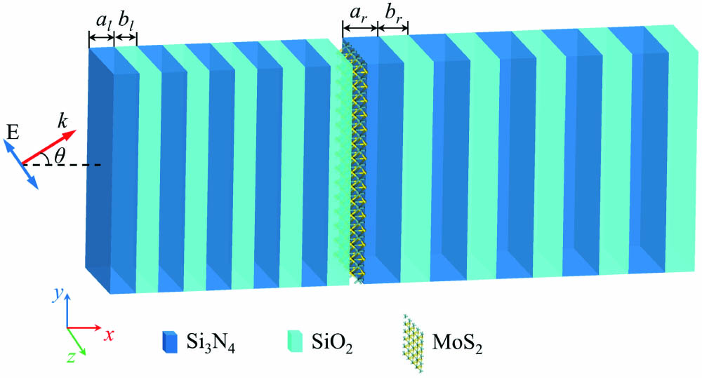
Figure 1 shows the proposed multilayer photonic structure with a monolayer sandwiched in two all-dielectric Bragg mirrors. The Bragg mirrors are composed of the alternatively stacked silicon nitride () and silica () layers, whose refractive indices are set as and , respectively[
Sign up for Chinese Optics Letters TOC. Get the latest issue of Chinese Optics Letters delivered right to you!Sign up now
![]()
Figure 1.Schematic diagram of the multilayer structure consisting of two different Bragg mirrors and a monolayer MoS2 sandwiched in the Bragg mirrors. The thicknesses of Si3N4 and SiO2 layers are denoted by al and bl (ar and br) for the left (right) Bragg mirror, respectively. The period numbers of the left and right Bragg mirrors are Pl and Pr, respectively. The light is incident from the left side of the structure.
The spectral response of multilayer structures can be theoretically calculated by the transfer matrix method (TMM)[
Based on Maxwell’s equations and the continuity of tangential components for electric and magnetic field vectors at the boundaries, the transfer matrices and can be derived to characterize the evolution of electric field amplitudes when light passes through the th interface and layer. They satisfy the relation as follows:
The reflection, transmission, and absorption spectra of the multilayer structure can be calculated by , , and , respectively. By using the above TMM, we investigate the light propagation characteristics of the multilayer structure with only two dielectric Bragg mirrors (i.e., ). The dielectric layer thicknesses of Bragg mirrors are set as , , , and . Thus, the bandgaps of two Bragg mirrors can be overlapped, providing an essential condition for the excitation of OTSs[
![]()
Figure 2.(a) Reflection spectra in the multilayer structure with Pl = 8, Pr = 20, al = 89 nm, bl = 44 nm, ar = 148 nm, br = 130 nm, and θ = 0°. (b) Light absorption spectra of the multilayer structure with a MoS2 monolayer. The lines and circles represent theoretical and simulation results, respectively. The upper inset shows the field distribution of |E|2 at the wavelength of 509.5 nm in the multilayer structure (h = 0 nm). The lower inset shows the spectrum of MoS2 light absorption in the full visible range.
3. Results and Analysis
Subsequently, we investigate the relation between the Bragg layer thickness and light absorption. Figure 3(a) depicts the evolution of the absorption spectrum with the thickness of the layer . Obviously, the absorption peak appears as a red shift with increasing and reaches the maximum when . The simulation results coincide well with the TMM calculations. As shown in Fig. 3(b), the absorption of monolayer can reach 95.3% with a full width at half-maximum (FWHM) of when . To clarify the physical mechanism of the light absorption improvement, we study the electric field intensities in between the Bragg mirrors with different , as plotted in the inset of Fig. 3(b). It is found that the electric field intensity exhibits a maximum when , which induces the strongest light- interaction and light absorption in the visible range. Furthermore, we investigate the dependence of light absorption on the thickness and incident angle . Figure 3(c) depicts the evolution of the absorption spectrum with when . It shows that the wavelength of the absorption peak possesses a red shift with increasing , and the absorption efficiency can reach the highest value of 95.7% when . With increasing the incident angle, there is a blue shift for the absorption peak, as shown in Fig. 3(d). The energy of OTSs rises when increasing [
![]()
Figure 3.(a) Evolution of MoS2 light absorption spectrum with the Si3N4 layer thickness al in the structure with ar = 148 nm and θ = 0°. (b) Corresponding absorption spectrum of MoS2 monolayer when al = 82 nm and θ = 0°. The inset shows the dependence of electric field intensity in MoS2 on al. (c) Evolution of MoS2 light absorption spectrum with the thickness ar when al = 82 nm and θ = 0°. (d) Evolution of MoS2 light absorption spectrum with θ when al = 82 nm and ar = 149 nm. The circles denote the simulation results. Here, Pl = 8, Pr = 20, bl = 44 nm, and br = 130 nm.
Moreover, we can see that the light absorption of relies on the period number of Bragg mirror , as depicted in Fig. 4(a). There is a slight blue shift for the absorption peak with increasing . The blue shift of the absorption peak arises from the deviation of OTS wavelengths with varying . The Bloch-wave-expansion method (BWEM) is introduced to obtain the precise OTS wavelengths and its dependence on the period numbers of two Bragg mirrors[
![]()
Figure 4.(a) Light absorption spectra of MoS2 monolayer in the multilayer structure with different period numbers Pl when Pr = 20. (b) Absorption peak values of MoS2 as a function of Pl, and the wavelengths of MoS2 absorption peak and OTS as a function of Pl. (c) Absorption spectra of MoS2 obtained by the TMM calculation (dots) and fitting (line) when Pl = 9. The inset shows the TCMT model of OTS in the structure. (d) Fitting parameters γ1, γ2, and γ3 versus Pl. (e) Absorption spectra of MoS2 in the structure with different Pr when Pl = 9. The inset shows the absorption spectra around the peaks. (f) Fitting parameters γ1, γ2, and γ3 versus Pr. Here, al = 82 nm, bl = 44 nm, ar = 149 nm, br = 130 nm, and θ = 0°.
Here, is the amplitude of the cavity mode. The reflection and transmission spectra can be achieved by and , respectively. Then, the absorption spectrum of can be obtained as
The above parameters , , and can be obtained by fitting the absorption spectra. Figure 4(c) shows the fitting absorption spectrum when , which is in good agreement with the theoretical result. The fitting results in Fig. 4(d) illustrate that the decay rate and loss rate exhibit a distinct drop with increasing . almost remains unchanged and is two orders of magnitude smaller than and (namely, , ). is closest to when , thereby the ratio of and can approach a maximum. Therefore, the light absorption can reach the highest value of 96.2% when .
Finally, we discuss the influence of period number on the light absorption. As shown in Fig. 4(e), the absorption shows an upward trend, and the increase of peak value slows down as increases. The peak value can approach 99.4% with an FWHM of 1.6 nm when . The peak wavelength remains unchanged with varying from 20 to 26. Compared to , is sufficiently large. The surface impedance at the interface of the right Bragg mirror barely changes in the overlapped band gap of Bragg mirrors. Thus, the wavelength with a minimum (corresponding to the OTS wavelength) remains at 504.9 nm, and the wavelength of the absorption peak is unchanged (506.0 nm). According to the BEWM calculation, the offset of the dip can be neglected when increases from 18. In other words, the position of the absorption peak will remain unchanged for . The fitting parameters in Fig. 4(f) show that still remains two orders of magnitude smaller than and . Meanwhile, and get closer to each other, giving rise to a higher ratio of and . Thereby, the absorption will be infinitely close to one with gradually increasing ().
4. Conclusions
We have investigated the enhanced visible light absorption of the monolayer sandwiched between two different Bragg mirrors with the excitation of the OTS mode. It is distinct from the cavity-supported light absorption enhancement in previous few-layer systems[
References
[1] A. Geim, K. Novoselov. The rise of graphene. Nat. Mater., 6, 183(2007).
[2] Z. Sun, H. Chang. Graphene and graphene-like two-dimensional materials in photodetection: mechanisms and methodology. ACS Nano, 8, 4133(2014).
[3] Z. Sun, A. Martinez, F. Wang. Optical modulators with 2D layered materials. Nat. Photon., 10, 227(2016).
[4] J. Ponraj, Z. Xu, S. Dhanabalan, H. Mu, Y. Wang, J. Yuan, P. Li, S. Thakur, M. Ashrafi, K. McCoubrey, Y. Zhang, S. Li, H. Zhang, Q. Bao. Photonics and optoelectronics of two-dimensional materials beyond graphene. Nanotechnology, 27, 462001(2016).
[5] T. Yang, H. Lin, B. Jia. Ultrafast direct laser writing of 2D materials for multifunctional photonics devices. Chin. Opt. Lett., 18, 023601(2020).
[6] K. Mak, J. Shan. Photonics and optoelectronics of 2D semiconductor transition metal dichalcogenides. Nat. Photon., 10, 216(2016).
[7] J. Pei, J. Yang, T. Yildirim, H. Zhang, Y. Lu. Many-body complexes in 2D semiconductors. Adv. Mater., 31, 1706945(2019).
[8] O. Lopez-Sanchez, D. Lembke, M. Kayci, A. Radenovic, A. Kis. Ultrasensitive photodetectors based on monolayer MoS2. Nat. Nanotechnol., 8, 497(2013).
[9] B. Radisavljevic, A. Radenovic, J. Brivio, V. Giacometti, A. Kis. Single-layer MoS2 transistors. Nat. Nanotechnol., 6, 147(2011).
[10] Y. Xie, B. Zhang, S. Wang, D. Wang, A. Wang, Z. Wang, H. Yu, H. Zhang, Y. Chen, M. Zhao, B. Huang, L. Mei, J. Wang. Ultrabroadband MoS2 photodetector with spectral response from 445 to 2717 nm. Adv. Mater., 29, 1605972(2017).
[11] H. Lu, Z. Yue, Y. Li, Y. Zhang, M. Zhang, W. Zeng, X. Gan, D. Mao, F. Xiao, T. Mei, W. Zhao, X. Wang, M. Gu, J. Zhao. Magnetic plasmon resonances in nanostructured topological insulators for strongly enhanced light-MoS2 interactions. Light Sci. Appl., 9, 191(2020).
[12] H. Zhang, S. Lu, J. Zheng, J. Du, S. Wen, D. Tang, K. Loh. Molybdenum disulfide (MoS2) as a broadband saturable absorber for ultra-fast photonics. Opt. Express, 22, 7249(2014).
[13] Y. Wang, D. Mao, X. Gan, L. Han, C. Ma, T. Xi, Y. Zhang, W. Shang, S. Hua, J. Zhao. Harmonic mode locking of bound-state solitons fiber laser based on MoS2 saturable absorber. Opt. Express, 23, 205(2015).
[14] M. Tsai, S. Su, J. Chang, D. Tsai, C. Chen, C. Wu, L. Li, L. Chen, J. He. Monolayer MoS2 heterojunction solar cells. ACS Nano, 8, 8317(2014).
[15] M. Long, E. Liu, P. Wang, A. Gao, H. Xia, W. Luo, B. Wang, J. Zeng, Y. Fu, K. Xu, W. Zhou, Y. Lv, S. Yao, M. Lu, Y. Chen, Z. Ni, Y. You, X. Zhang, S. Qin, Y. Shi, W. Hu, D. Xing, F. Miao. Broadband photovoltaic detectors based on an atomically thin heterostructure. Nano Lett., 16, 2254(2016).
[16] J. R. Piper, S. Fan. Broadband absorption enhancement in solar cells with an atomically thin active layer. ACS Photon., 3, 571(2016).
[17] W. Wang, A. Klots, Y. Yang, W. Li, I. Kravchenko, D. Briggs, K. Bolotin, J. Valentine. Enhanced absorption in two-dimensional materials via Fano-resonant photonic crystals. Appl. Phys. Lett., 106, 181104(2015).
[18] S. Bahauddin, H. Robatjazi, I. Thomann. Broadband absorption engineering to enhance light absorption in monolayer MoS2. ACS Photon., 3, 853(2016).
[19] X. Luo, X. Zhai, L. Wang, Q. Lin. Enhanced dual-band absorption of molybdenum disulfide using a plasmonic perfect absorber. Opt. Express, 26, 11658(2018).
[20] C. Janisch, H. Song, C. Zhou, Z. Lin, A. L. Elías, D. Ji, M. Terrones, Q. Gan, Z. Liu. MoS2 monolayers on nanocavities: enhancement in light-matter interaction. 2D Mater., 3, 025017(2016).
[21] L. Zhu, F. Liu, H. Lin, J. Hu, Z. Yu, X. Wang, S. Fan. Angle-selective perfect absorption with two-dimensional materials. Light Sci. Appl., 5, e16052(2016).
[22] J. Hu, J. Fu, X. Liu, D. Ren, J. Zhao, Y. Huang. Perfect absorption in a monolayer graphene at the near-infrared using a compound waveguide grating by robust critical coupling. Chin. Opt. Lett., 17, 010501(2019).
[23] D. Jariwala, A. Dayoyan, G. Tagliabue, M. Sherrott, J. Wong, H. Atwater. Near-unity absorption in van der Waals semiconductors for ultrathin optoelectronics. Nano Lett., 16, 5482(2016).
[24] Z. Liu, K. Aydin. Localized surface plasmons in nanostructured monolayer black phosphorus. Nano Lett., 16, 3457(2016).
[25] A. Kavokin, I. Shelykh, G. Malpuech. Lossless interface modes at the boundary between two periodic dielectric structures. Phys. Rev. B, 72, 233102(2005).
[26] T. Goto, A. Dorofeenko, A. Merzlikin, A. Baryshev, A. Vinogradov, M. Inoue, A. Lisyansky, A. Granovsky. Optical Tamm states in one-dimensional magnetophotonic structures. Phys. Rev. Lett., 101, 113902(2008).
[27] F. Chien, J. Chang, S. Lin, Y. Chou, T. Chen, S. Gwo, T. Chao, W. Hsieh. Nanometer-scale conversion of Si3N4 to SiOx. Appl. Phys. Lett., 76, 360(2000).
[28] J. Xi, J. Kim, E. Schubert. Silica nanorod-array films with very low refractive indices. Nano Lett., 5, 1385(2005).
[29] M. Furchi, A. Urich, A. Pospischil, G. Lilley, K. Unterrainer, H. Detz, P. Klang, A. Andrews, W. Schrenk, G. Strasser, T. Mueller. Microcavity-integrated graphene photodetector. Nano Lett., 12, 2773(2012).
[30] Y. Li, A. Chernikov, X. Zhang, A. Rigosi, H. Hill, A. van der Zande, D. Chenet, E. Shih, J. Hone, T. Heinz. Measurement of the optical dielectric function of monolayer transition-metal dichalcogenides: MoS2, MoSe2, WS2, and WSe2. Phys. Rev. B, 90, 205422(2014).
[31] N. Ansari, F. Ghorbani. Light absorption optimization in two-dimensional transition metal dichalcogenide van der Waals heterostructures. J. Opt. Soc. Am. B, 35, 1179(2018).
[32] M. Kaliteevski, I. Iorsh, S. Brand, R. Abram, J. Chamberlain, A. Kavokin, I. Shelykh. Tamm plasmon-polaritons: possible electromagnetic states at the interface of a metal and a dielectric Bragg mirror. Phys. Rev. B, 76, 165415(2007).
[33] H. Lu, Y. Li, Z. Yue, D. Mao, J. Zhao. Graphene-tuned EIT-like effect in photonic multilayers for actively controlled light absorption of topological insulators. Opt. Express, 28, 31893(2020).
[34] H. Lu, X. Gan, B. Jia, D. Mao, J. Zhao. Tunable high-efficiency light absorption of monolayer graphene via Tamm plasmon polaritons. Opt. Lett., 41, 4743(2016).
[35] A. Taflove, S. Hagness. Computational Electrodynamics: the Finite-difference Time-domain Method(2005).
[36] X. Kang, W. Tan, Z. Wang, H. Chen. Optic Tamm states: The Bloch-wave-expansion method. Phys. Rev. A, 79, 043832(2009).
[37] J. Joannopoulos, S. Johnson, J. Winn, R. Meade. Photonic Crystals: Molding the Flow of Light(2008).
[38] M. Kats, F. Capasso. Optical absorbers based on strong interference in ultra-thin films. Laser Photon. Rev., 10, 735(2016).

Set citation alerts for the article
Please enter your email address
© Copyright 2018-2021 | Chinese Laser Press. All Rights Reserved 沪ICP备15018463号-20