
Tang Jia, Li Jiaxiang, Chen Qin, Wen Long. Surface Plasmon Enhanced Silicon-Based Near-Infrared Photoconductive Detector[J]. Chinese Journal of Lasers, 2020, 47(11): 1113002
- Chinese Journal of Lasers
- Vol. 47, Issue 11, 1113002 (2020)
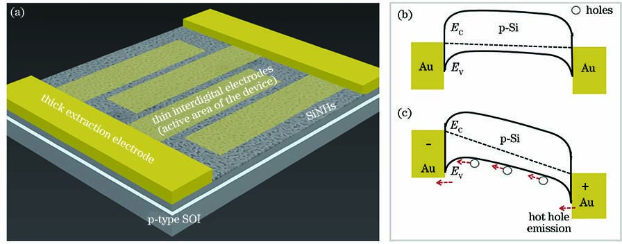
Fig. 1. Structural and band diagrams of device. (a) Schematic of surface plasmon enhanced silicon-based near-infrared photoconductive detector; (b) band diagram of detector under zero voltage bias; (c) band diagram of detector under external voltage bias
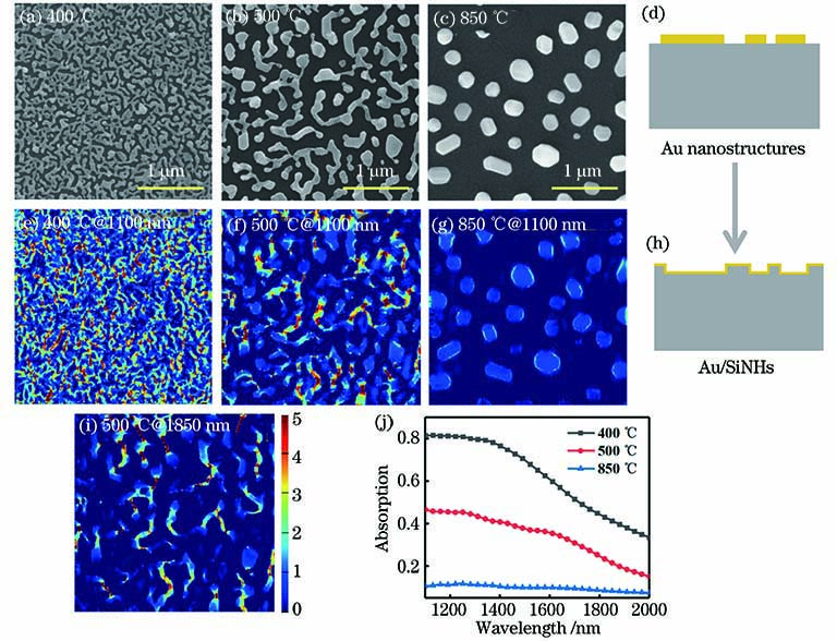
Fig. 2. Design and simulation of disordered metal nanostructures. (a)--(c) Scanning electron microscopy (SEM) images of Au nanostructures with different thermal dewetting temperatures; (d) side diagram of Au nanostructure formed after thermal annealing for film; (e)--(g) simulated electric fields of Au/SiNHs structures corresponding to images in Figs. 2(a)--(c) at 1100 nm incident light; (h) side diagram of Au/SiNHs structure; (i) simulated electric field of Au/SiNHs structure corresponding to image in
Fig. 3. Fabrication procedure for the proposed photodetectors
Fig. 4. Microscope pictures of important steps in device fabrication procedure. (a) SEM image of disordered banded structure after annealing; (b) SEM image of disordered banded SiNHs structure; optical microscope pictures with (c) thin interdigital electrode and (d) thick extraction electrode
Fig. 5. Test schematic diangram and electrical test results of device. (a) Schematic diagram of device test; (b) I-V characteristic curve of device under dark state. The upper left inset is picture of device, and lower right inset is diagram of interdigitated electrode
Fig. 6. Test of device photoelectric conversion performance. (a) Time-resolved photocurrent spectra of detector and planar reference device under relevant bias voltage and corresponding incident light wavelengths; (b) photocurrent response spectra of detector and planar reference device under relevant bias voltage

Set citation alerts for the article
Please enter your email address
© Copyright 2018-2021 | Chinese Laser Press. All Rights Reserved 沪ICP备15018463号-20