
Li ZHOU, Xiaohu ZHANG, Xiaogang LIN, Chao GAO, Yongcai GUO. A Planar Artificial Compound Eye Based on Metalens Array[J]. Acta Photonica Sinica, 2021, 50(6): 168
- Acta Photonica Sinica
- Vol. 50, Issue 6, 168 (2021)
Abstract
Keywords
GUO Yongcai (1963-), female, professor, Ph.D. degree, mainly focuses on environmental monitoring, light scattering theory and so on. Email: ycguo@cqu.edu.cn
0 Introduction
The traditional optical systems are usually single-aperture systems which are consisted of bulky optical elements with elaborate designs to eliminate aberrations and improve imaging qualities, such as doublet lenses and aspheric lenses. Benefitting from those excellent properties, they are widely used in many scenarios. However, some applications of rapid development (like drones and endoscopy imaging) in recent years have raised higher demands for the imaging system, such as light weight, small size, and large Field Of View (FOV). The bulky volumes and heavy weights of traditional optical systems make them difficult to be miniaturized and integrated. A new methodology which can simultaneously realize the miniaturization and large FOV of the image systems is highly expected in the optical field.
To achieve such goals, Artificial Compound Eyes (ACEs) were developed based on the structures of the biotic compound eyes for their features including compact structure and large FOV[
In this work, a planar ACE structure is proposed based on the utilization of metalenses. Metasurface lens (metalens)[
1 Design process of ACE
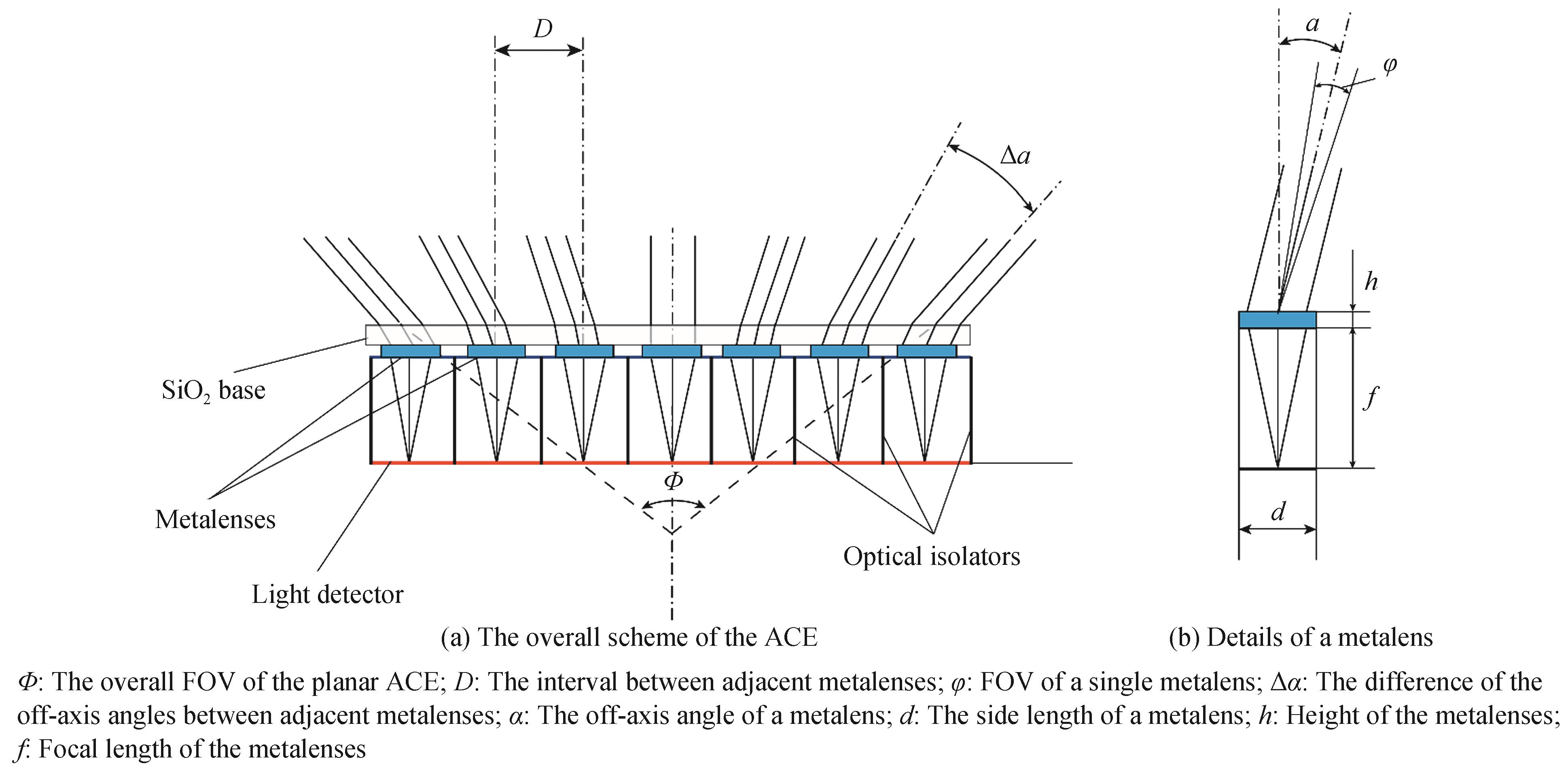
1.1 Schematic of the ACE
The detailed layout of the proposed planar ACE is shown in Fig.1. It comprises a single layer of planar MA, which is usually supported by a layer of transparent base (which is silicon dioxide (SiO2) in this work) and a light receiver focal plane to collect the generated subimages. The MA is composed of metalenses to generate the subimages of different portions of the object field. The metalenses are designed with a side length d=10.2 μm and height h=0.6 μm. The FOV of a single metalens φ reaches 40º according to the simulation results, and it is here taken as φ=40º. In addition to focusing, each metalens is designed with an off-axis angle α, which represents its off-axis angle in the object space. When the incident direction is parallel to the metalens’ off-axis direction, the transmitted light beams are normally focused onto the focal plane. Thus, a portion of the object field (α-φ/2, α+φ/2) is transferred successfully. The inter-ommatidia angle Δα is defined as the difference of the off-axis angles between adjacent metalenses. With Δα set smaller than φ to eliminate blind areas, the overall FOV of the MA Φ can reach ±(αmax+φ/2), where αmax is the maximum off-axis angle. To prevent crosstalk, optical isolators should be added between adjacent channels[
![]()
Figure 1.The scheme of the planar ACE
1.2 The optical performance of the subwavelength structure
The metalenses used to construct the MA is a newly developed planar lens that controls light based on the geometric phase. The geometric phase, also named as Pancharatnam-Berry (PB) phase, is always frequency-independent and can be conveniently implemented through the rotation of the nano-structures[
![]()
Figure 2.Details of the nanopillars
Under the normal incidence of Left Circular Polarized (LCP) light at 467.5 nm wavelength, the amplitude and phase response of the transmitted cross-polarization light, which in this case is the Right Circular Polarized (RCP) light, is calculated and shown in Fig.2(b). The amplitude is above 99% and the phase is almost in a linear relation with the rotation angle, which agrees with the geometric phase anticipation. Fig. 2(c) shows the phase shift of the transmitted cross-polarization light produced by nanopillars with different orientation angles throughout the visible wavelength. The phase of the nanopillar with 0° orientation is set zero as the baseline. It can be seen that the relative phase shift is almost in linear relation with the orientation angle in the wavelength from 450 nm to 700 nm. The broadband amplitude responses of the proposed nanopillars are shown in Fig.2(d). Although the amplitude responses are different for the variation of the incident wavelengths, the cross-polarized amplitude nearly keeps constant with the change of the orientation angles. The broadband properties shown in Fig.2(c) and Fig.2(d) prove that the designed nanopillar can be operated in a broad wavelength range. The phase responses and average amplitude of the transmitted cross-polarization light for the off-axis illumination are shown in Fig.2(e) and (f). It can be seen that the phase shift produced by the nanopillars with an incident angle is similar to the normal incidence situation and basically follows a linear relation with the orientation angle of the unit structure (some deviations at large off-axis angles will not affect focus seriously because of the tolerance of the metalenses[
1.3 Metalens design
The metalenses are constructed with numerous nanopillars to modulate the phase of the transmitted light. In order to realize a planar ACE, the constructed metalenses focus the incident light with different inclination angles with an acceptable transmittance. According to the equal optical path principle, to focus the normally incident plane wave, the abrupt phase shift generated by nanopillars on the metalens should be a part-spherical shell[
![]()
Figure 3.Details of the metalens
where ω(x,y) is the needed abrupt phase shift on different positions of the metalens, x and y are coordinates on the metalens, λ is the working wavelength (467.5 nm, which is also the wavelength of the Ar-Kr laser), f is the focal length (18 μm), m is an integer to make sure that the final value is within the range 0~2π.
To counteract the effect of the incident light's inclination on the focusing performance, the wavefront of the transmitted light needs to remain a part-spherical shell. As is shown in Fig.3(b), similar to the traditional method of adding a glass wedge to steer light beams[
where θ(x,y) is the nanopillars' orientation angle at different positions on the metalens. Fig. 3(d) shows an example of the metalens with the off-axis angle α=30º, focal length f=18 μm and size length d=10.2 μm. It is constructed with an array of 34×34 TiO2 nanopillars. High-throughput lithography methods, such as deep-ultraviolet[
2 Simulation
The FOV of a single metalens is very important for the imaging ability of the proposed planar ACE. The bigger it is, the less metalenses are needed to cover a large FOV. For metalenses, their FOVs are difficult to be acquired using the traditional glass-based formulas. In order to determine the FOV of the 0° off-axis metalens, the Point Spread Functions (PSFs) under different incidence angles are analyzed. Here, the electric fields of the metalenses are simulated and observed using the CST Microwave Studio. It should be noted that, because of the limited computing resources, direct calculation of the light field distribution at the focal plane is extremely difficult. To handle the problem, the near-field light field distribution on the plane of 0.5 µm above the metalens is extracted. Subsequently, the field distribution of the final focal spot is calculated using the vectorial angular spectrum theory[
![]()
Figure 4.The performance of the 0° off-axis metalens with inclined illumination. The intensities have been normalized with the maximum intensity in (a)
To verify the feasibility of the proposed ACE structure, the optical performances of all the composed off-axis metalenses should be evaluated. However, although the metalenses are designed with different off-axis angles, their basic structures are similar. Here, three metalenses with the off-axis angles of 0º,30º and 50º are chosen to verify the feasibility of the MA. For each metalens, the incident angle is set equal to its off-axis angle, making the emergent light normally focus onto the focal plane. The focusing intensity distribution and PSFs of the three metalenses are demonstrated in Fig.5(a)~(f). The FWHMs of the 0°, 30° and 50° off-axis metalenses are 0.74 μm, 0.74 μm and 0.75 μm, respectively. The FWHM of the 50º off-axis metalens is nearly the same as the 0º off-axis metalens, indicating that the imaging abilities of the metalenses are almost constant at large off-axis angles. The focusing efficiency is calculated by Efoci/Einci, where Efoci is the energy within the first zero point, and Einci is the overall incident energy. The focusing efficiencies of the 3 metalenses are 75.5%, 46.8% and 20.9%, respectively. The drop of the focusing efficiency at large off-axis angles indicate that fewer light beams are focused into the focal spot as the off-axis angle increases, and that the image quality and intensity may be reduced. However, the intensity differences for metalenses with large off-axis angles can be relieved through reverse-compensation in the post-treatment process.
![]()
Figure 5.The focusing performance of the 0º, 30º and 50º off-axis metalens. The intensities have been normalized with the maximum intensity in (a)
To verify the imaging ability, imaging simulation of all three metalenses are conducted using convolution computation. Here, two 1 μm-diameter points with the interval of 2 μm are taken as the object to generate the respective images. Fig. 6(a) shows the intensity distribution of the original 2-point object and its cross section (shown in the inset). Fig. 6(b), (c) and (d) showed the produced images and their cross sections (shown in the insets) for the 0º, 30º and 50º metalenses, respectively. It can be seen that despite some overlapping, the produced images of the 2-point object are discriminable, proving the off-axis metalenses’ feasibility for imaging.
![]()
Figure 6.Imaging simulation with the two-point object. The intensities have been normalized with the maximum intensity in (b)
A more complicated picture (the badge of Chongqing University (Fig. 7 (a)) is chosen as the object to further verify the feasibility of the proposed scheme. The imaging performance of the 0º, 30º and 50º metalenses are shown in Fig. 7(b) ~(d). It can be seen that, although the image quality of the 50º off-axis metalens is mildly poorer, it can still be regarded as visible because the badge details remain recognizable after transmission. The reason for the degradation of the image quality is that the noise of the background is increased and the focusing efficiency is dropped with the increase of the incident angle. Although the imaging abilities of metalenses are influenced by the off-axis angle to some extent, it is good enough to produce a clear image of a complicated object.
![]()
Figure 7.Imaging simulation with the badge object. The intensities have been normalized with the maximum intensity in (b)
A comparison of different ACE structures is shown in Table 1. Some parameters are compared including the surface type (planar/ 3D), layer number (number of the optical device layers), FOV (the overall FOV of the ACE), size (the size of the whole ACE), and overall height (the distance between the first layer of optical device and the image plane). It can be seen that the proposed metalens-based planar ACE obtains a large FOV with a single-layered planar structure. Due to the compact structure of metalenses, the geometric dimensions of the ACE are also extremely small.
| ACE Design | Surface | Layer number | FOV | Size/μm | Overall height |
|---|---|---|---|---|---|
| This work | Planar | 1 | 140°×140° | 165×165 | 18.6 μm |
| 3-layer planar ACE[ | Planar | 3 | 70°×10° | 4500×500 | 2 mm |
| Prism-based planar ACE[ | Planar | 4 | 30°×30° | - | 24.8 mm |
| Flexible zoom ACE [ | 3D | 1 | - | Diameter=8 660 | 2.283 mm |
| 3D ACE using laser scanning[ | 3D | 1 | 90°×90° | Diameter=84 | 20 μm |
| 3D ACE using polymerization[ | 3D | 2 | 107.48°×97.97° | 30×30 | 15 μm |
Table 1. The comparison of different ACE designs
3 Conclusion
In this work, a scheme to realize a planar ACE with a large FOV is proposed. It is composed of a transparent SiO2 substrate to hold the whole structure, a receiver to collect the produced images, and a metalens array, which uses metalenses in this work to image different portions of the object field. Although a single metalens covers a limited FOV, the combined image of the metalenses cover a large FOV with proper arrangement of the off-axis angles of the metalenses, which reaches as large as 140º×140° in this work. Importantly, because the off-axis angle is embedded within the structure of the metalenses, they do not require additional components to aim for different fields. The metalenses and their produced subimages both lie on a planar plane, making it beneficial for designing and manufacturing as no complicated curving process or any intermediate devices are required. In practical use, the intensity difference between the subimages should be compensated in the post-treatment process to avoid abrupt change of local brightness. Combined with the fast development of metasurfaces, the metasurfaces-based ACEs allow for not only large FOV and compact size, but also color imaging ability[
References
[1] S FISCHER, C H G MULLER, V B MEYER-ROCHOW. How small can small be: The compound eye of the parasitoid wasp Trichogramma evanescens (Westwood, 1833) (Hymenoptera, Hexapoda), an insect of 0.3-to 0.4-mm total body size. Visual Neuroscience, 28, 295-308(2011).
[2] K STOLLBERG, A BRUCKNER, J DUPARRE et al. The Gabor superlens as an alternative wafer-level camera approach inspired by superposition compound eyes of nocturnal insects. Optics Express, 17, 15747-15759(2009).
[3] M FRIEDRICH, S BENZER. Divergent decapentaplegic expression patterns in compound eye development and the evolution of insect metamorphosis. Journal of Experimental Zoology, 288, 39-55(2000).
[4] Lin ZHU, Yuanyuan GAO, Xinyu HU et al. Progress in femtosecond laser fabrication of artificial compound eye. Chinese Science Bulletin, 64, 1254-1267(2019).
[5] H JUNG, K H JEONG. Microfabricated ommatidia using a laser induced self-writing process for high resolution artificial compound eye optical systems. Optics Express, 17, 14761-14766(2009).
[6] KUO Wenkai, KUO Guanfu, S Y LIN et al. Fabrication and characterization of artificial miniaturized insect compound eyes for imaging. Bioinspiration & Biomimetics, 10(2015).
[7] Shuqing ZHANG, Luyang ZHOU, Changxi XUE et al. Design and simulation of a superposition compound eye system based on hybrid diffractive-refractive lenses. Applied Optics, 56, 7442-7449(2017).
[8] H R FALLAH, A KARIMZADEH. Design and simulation of a high-resolution superposition compound eye. Journal of Modern Optics, 54, 67-76(2007).
[9] J W LEEM, Y M SONG, J S YU. Biomimetic artificial Si compound eye surface structures with broadband and wide-angle antireflection properties for Si-based optoelectronic applications. Nanoscale, 5, 10455-10460(2013).
[10] Lun LI, Yongping HAO, Jiulong XU et al. The design and positioning method of a flexible zoom artificial compound eye. Micromachines (Basel), 9, 319(2018).
[11] G DRUART, N GUÉRINEAU, R HAÏDAR et al. Demonstration of an infrared microcamera inspired by xenos peckii vision. Applied Optics, 48, 3368-3374(2009).
[12] J DUPARRE, P SCHREIBER, A E MATTHES et al. Microoptical telescope compound eye. Optics Express, 13, 889-903(2005).
[13] M KHORASANINEJAD, Z SHI, A Y ZHU et al. Achromatic metalens over 60 nm bandwidth in the visible and metalens with reverse chromatic dispersion. Nano Letter, 17, 1819-1824(2017).
[14] Xiaoliang MA, Mingbo PU, Xiong LI et al. All-metallic wide-angle metasurfaces for multifunctional polarization manipulation. Opto-Electronic Advances, 2, 180023(2019).
[15] Jingying GUO, Teng WANG, Baogang QUAN et al. Polarization multiplexing for double images display. Opto-Electronic Advances, 2, 180029(2019).
[16] N I ZHELUDEV, Y S KIVSHAR. From metamaterials to metadevices. Nature Materials, 11, 917-924(2012).
[17] Hao ZHANG, Lei LI, D L MCCRAY et al. Development of a low cost high precision three-layer 3D artificial compound eye. Optics Express, 21, 22232-22245(2013).
[18] A KARIMZADEH. Optical design of high resolution concave superposition compound eye. Osa Continuum, 2, 3044-3049(2019).
[19] J DUPARRE, P DANNBERG, P SCHREIBER et al. Thin compound-eye camera. Applied Optics, 44, 2949-2956(2005).
[20] S HERMON, A MA, Fuyong YUE et al. Metasurface hologram for polarization measurement. Optics Letters, 44, 4436-4438(2019).
[21] B H CHEN, P C WU, V C SU et al. GaN metalens for pixel-level full-color routing at visible light. Nano Letters, 17, 6345-6352(2017).
[22] J P B MUELLER, N A RUBIN, R C DEVLIN et al. Metasurface polarization optics: independent phase control of arbitrary orthogonal states of polarization. Physical Review Letters, 118, 113901(2017).
[23] R C DEVLIN, M KHORASANINEJAD, W T CHEN et al. Broadband high-efficiency dielectric metasurfaces for the visible spectrum. Proceedings of the National Academy of Sciences, 113, 10473-10478(2016).
[24] Xiaohu ZHANG, Jinjin JIN, Mingbo PU et al. Ultrahigh-capacity dynamic holographic displays via anisotropic nanoholes. Nanoscale, 9, 1409-1415(2017).
[25] Deli CHEN, Junjie WANG, Yongle QI et al. Polarization-insensitive dielectric metalenses with different numerical apertures and off-axis focusing characteristics. Journal of the Optical Society of America B, 37, 3588-3595(2020).
[26] M KHORASANINEJAD, W T CHEN et al. Super-dispersive off-axis meta-lenses for compact high resolution spectroscopy. Nano Letters, 16, 3732-3737(2016).
[27] P SERGAN et al. Wide-angle achromatic prism beam steering for infrared countermeasure applications. Optical Engineering, 42, 1038-1047(2003).
[28] J S PARK, Shuyan ZHANG, A SHE et al. All-glass, large metalens at visible wavelength using deep-ultraviolet projection lithography. Nano Letters, 19, 8673-8682(2019).
[29] M KHORASANINEJAD, W T CHEN, R C DEVLIN et al. Metalenses at visible wavelengths: Diffraction-limited focusing and subwavelength resolution imaging. Science, 352, 1190-1194(2016).
[30] Zhibin FAN, Haoyang QIU, Hanle ZHANG et al. A broadband achromatic metalens array for integral imaging in the visible. Light: Science& Applications, 8, 67(2019).
[31] Dongliang TANG, Long CHEN, Jianjun LIU. Visible achromatic super-oscillatory metasurfaces for sub-diffraction focusing. Optics Express, 27, 12308-12316(2019).
[32] Dongliang TANG, Jia LIU, Long CHEN et al. Reflective plasmonic super-oscillatory metasurfaces with simultaneous phase and amplitude controls for sub-diffraction focusing. Journal of Physics D:Applied Physics, 53, 154001(2020).
[33] Rao FU, Zile LI, Guoxing ZHENG et al. Reconfigurable step-zoom metalens without optical and mechanical compensations. Optics Express, 27, 12221-12230(2019).
[34] Dong WU, Jiannan WANG, Ligang NIU et al. Bioinspired Fabrication of high-quality 3D artificial compound eyes by voxel-modulation femtosecond laser writing for distortion-free wide-field-of-view imaging. Advanced Optical Materials, 2, 751-758(2014).
[35] Jieqiong LIN, Yudi KAN, Xian JING et al. Design and fabrication of a three-dimensional artificial compound eye using two-photon polymerization. Micromachines, 9, 336(2018).
[36] S COLBURN, A ZHAN, A MAJUMDAR. Metasurface optics for full-color computational imaging. Science Advances, 4, eaar2114(2018).
[37] M MIYATA, M NAKAJIMA, T HASHIMOTO. Compound-eye metasurface optics enabling a high-sensitivity, ultra-thin polarization camera. Optics Express, 28, 9996-10014(2020).

Set citation alerts for the article
Please enter your email address
© Copyright 2018-2021 | Chinese Laser Press. All Rights Reserved 沪ICP备15018463号-20