• Photonics Research
  • Vol. 9, Issue 9, 1745 (2021)
Kai Sun1、2、†, Zi-Jian Zhang3、†, Fei Meng3、4, Bin Cheng3、5, Zhu Cao6, Jin-Shi Xu1、2、9、*, Man-Hong Yung3、7、8、10、*, Chuan-Feng Li1、2、11、*, and Guang-Can Guo1、2
Author Affiliations
  • 1CAS Key Laboratory of Quantum Information, University of Science and Technology of China, Hefei 230026, China
  • 2CAS Center for Excellence in Quantum Information and Quantum Physics, University of Science and Technology of China, Hefei 230026, China
  • 3Department of Physics, Southern University of Science and Technology, Shenzhen 518055, China
  • 4Department of Computer Science, The University of Hong Kong, Pokfulam, Hong Kong SAR, China
  • 5Centre for Quantum Software and Information, Faculty of Engineering and Information Technology, University of Technology Sydney, Sydney, NSW 2007, Australia
  • 6Key Laboratory of Advanced Control and Optimization for Chemical Processes of Ministry of Education, East China University of Science and Technology, Shanghai 200237, China
  • 7Shenzhen Institute for Quantum Science and Engineering, Southern University of Science and Technology, Shenzhen 518055, China
  • 8Shenzhen Key Laboratory of Quantum Science and Engineering, Southern University of Science and Technology, Shenzhen 518055, China
  • 9e-mail: jsxu@ustc.edu.cn
  • 10e-mail: yung@sustech.edu.cn
  • 11e-mail: cfli@ustc.edu.cn
  • show less
    DOI: 10.1364/PRJ.427897 Cite this Article Set citation alerts
    Kai Sun, Zi-Jian Zhang, Fei Meng, Bin Cheng, Zhu Cao, Jin-Shi Xu, Man-Hong Yung, Chuan-Feng Li, Guang-Can Guo. Experimental verification of group non-membership in optical circuits[J]. Photonics Research, 2021, 9(9): 1745 Copy Citation Text show less
    Core circuit. The circuit is similar to the swap test circuit and aims to check whether the input state is invariant under certain group multiplication. With a correct proof state, if x∈S, the measurement outcome is always 0; if x∉S, the measurement outcome is 1 with probability 0.5.
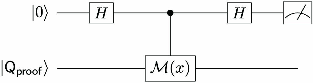
    Fig. 1. Core circuit. The circuit is similar to the swap test circuit and aims to check whether the input state is invariant under certain group multiplication. With a correct proof state, if xS, the measurement outcome is always 0; if xS, the measurement outcome is 1 with probability 0.5.
    Circuit mapping and experimental setup. (a) The circuits for group multiplications in the first line are deduced from the quantum labels for the elements. They are used to construct the core circuits for the verification process in the second line. Optical paths are presented in the third line. Here, two BSs building an MZI are used to play the role of two Hadamard operations on the control qubit, which is realized with the path information. One path is regarded as |0⟩ and the other one is |1⟩. An HWP is placed in |1⟩ path to act as the CNOT gate on the polarization qubit with the optical axis at 45°. (b) Experimental setups. Entangled photon pairs are produced by pumping BBO and using quartz plates (QPs) on the above panel. Two photons are sent to the sides a and b respectively. On each side, an SI, shown on the bottom panel in detail, is constructed to realize the MZI. In an SI, an HWP is placed in |1⟩ path (shown in orange beam and marked as 2) and a phase compensation (PC) crystal is located in |0⟩ (shown in blue beam and marked as 1). A measurement unit (MU) consisting of a QWP, an HWP, a PBS, and a single-photon detector (D) equipped with an interferometer filter (IF) is placed on each output port (marked as 3 and 4) of the SI. Note, in this figure, unitary of multiplying by A is realized. By removing the SI, we can implement different quantum circuits.
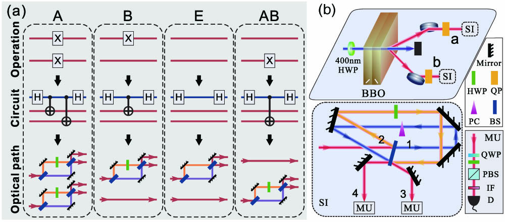
    Fig. 2. Circuit mapping and experimental setup. (a) The circuits for group multiplications in the first line are deduced from the quantum labels for the elements. They are used to construct the core circuits for the verification process in the second line. Optical paths are presented in the third line. Here, two BSs building an MZI are used to play the role of two Hadamard operations on the control qubit, which is realized with the path information. One path is regarded as |0 and the other one is |1. An HWP is placed in |1 path to act as the CNOT gate on the polarization qubit with the optical axis at 45°. (b) Experimental setups. Entangled photon pairs are produced by pumping BBO and using quartz plates (QPs) on the above panel. Two photons are sent to the sides a and b respectively. On each side, an SI, shown on the bottom panel in detail, is constructed to realize the MZI. In an SI, an HWP is placed in |1 path (shown in orange beam and marked as 2) and a phase compensation (PC) crystal is located in |0 (shown in blue beam and marked as 1). A measurement unit (MU) consisting of a QWP, an HWP, a PBS, and a single-photon detector (D) equipped with an interferometer filter (IF) is placed on each output port (marked as 3 and 4) of the SI. Note, in this figure, unitary of multiplying by A is realized. By removing the SI, we can implement different quantum circuits.
    Real parts of density matrices of the final output photons for the case with input state of (|HH⟩+|VV⟩)/2. (a)–(c) Cases of initial state, output photons of a3 and b in E-type interferometer, output photons of a and b3 in AB-type interferometer without CNOT gate, respectively; (e)–(g) cases of output photons of a3 and b3 in A-type interferometer (with fidelity 92.6%±2.4%), a3 and b in B-type interferometer (88.9%±0.7%), a and b3 in AB-type interferometer (88.5%±1.2%), respectively; (i)–(k) cases of output photons of a4 and b4 in A-type interferometer (98.0%±0.3%), a4 and b in B-type interferometer (94.4%±0.3%), a and b4 in AB-type interferometer (94.8%±0.9%), respectively; (d), (h), and (l) corresponding theoretical predictions.
    Fig. 3. Real parts of density matrices of the final output photons for the case with input state of (|HH+|VV)/2. (a)–(c) Cases of initial state, output photons of a3 and b in E-type interferometer, output photons of a and b3 in AB-type interferometer without CNOT gate, respectively; (e)–(g) cases of output photons of a3 and b3 in A-type interferometer (with fidelity 92.6%±2.4%), a3 and b in B-type interferometer (88.9%±0.7%), a and b3 in AB-type interferometer (88.5%±1.2%), respectively; (i)–(k) cases of output photons of a4 and b4 in A-type interferometer (98.0%±0.3%), a4 and b in B-type interferometer (94.4%±0.3%), a and b4 in AB-type interferometer (94.8%±0.9%), respectively; (d), (h), and (l) corresponding theoretical predictions.
    Imaginary parts of density matrices of the final output photons for the case with input state of 12(|HH⟩+|VV⟩). (a)–(c) Cases of initial state, output photons of a3 and b in E-type interferometer, output photons of a and b3 in AB-type interferometer without CNOT gate, respectively; (e)–(g) cases of output photons of a3 and b3 in A-type interferometer, a3 and b in B-type interferometer, a and b3 in AB-type interferometer, respectively; (i)–(k) cases of output photons of a4 and b4 in A-type interferometer, a4 and b in B-type interferometer, a and b4 in AB-type interferometer, respectively; (d), (h), and (l) corresponding theoretical predictions.
    Fig. 4. Imaginary parts of density matrices of the final output photons for the case with input state of 12(|HH+|VV). (a)–(c) Cases of initial state, output photons of a3 and b in E-type interferometer, output photons of a and b3 in AB-type interferometer without CNOT gate, respectively; (e)–(g) cases of output photons of a3 and b3 in A-type interferometer, a3 and b in B-type interferometer, a and b3 in AB-type interferometer, respectively; (i)–(k) cases of output photons of a4 and b4 in A-type interferometer, a4 and b in B-type interferometer, a and b4 in AB-type interferometer, respectively; (d), (h), and (l) corresponding theoretical predictions.
    Experimental results. (a), (c) Detecting probabilities of |0⟩ with different input proof states for the circuit A and AB, respectively; (b), (d) probability for the proof states |Qproof⟩ and |Q′proof⟩ to prove GNM for every group element (detecting the control qubit in |1⟩). The histograms and black points are theoretical and experimental results, respectively. All error bars are estimated to be standard deviation from the statistical variation of the photon counts, assumed to follow a Poisson distribution.
    Fig. 5. Experimental results. (a), (c) Detecting probabilities of |0 with different input proof states for the circuit A and AB, respectively; (b), (d) probability for the proof states |Qproof and |Qproof to prove GNM for every group element (detecting the control qubit in |1). The histograms and black points are theoretical and experimental results, respectively. All error bars are estimated to be standard deviation from the statistical variation of the photon counts, assumed to follow a Poisson distribution.
    Kai Sun, Zi-Jian Zhang, Fei Meng, Bin Cheng, Zhu Cao, Jin-Shi Xu, Man-Hong Yung, Chuan-Feng Li, Guang-Can Guo. Experimental verification of group non-membership in optical circuits[J]. Photonics Research, 2021, 9(9): 1745
    Download Citation