Abstract
In a single nanoscale device, surface plasmon polaritons (SPPs) have potential to match the different length scales associated with photonics and electronics. In this Letter, we propose an accurate design of a plasmonic metasurface Luneburg lens (PMLL) accommodating SPPs. The simulations indicate that the full width at half-maximum is 0.42 μm, and the focus efficiency is 78%. The characters of a PMLL have robustness to manufacturing errors. The PMLL is applied in a 10 μm long compact coupler model, which couples the SPPs to the 40 nm wide output waveguide. The couple efficiency is higher than that of a conventional taper coupler in a broad bandwidth. The design is compatible with standard lithography technology.With the development of the photonic integrated circuit, it is respected to integrate optical devices and electronic devices in a single chip[1,2]. The most challenging problem is the different length scales between photonics and electronics. The diameter of standard single-mode fibers in the telecom industry is 9 μm. The electronic elements in the integrated circuit are with nanoscale (). Surface plasmon polaritons (SPPs) are considered to be the most possible solutions[3]. SPPs are electromagnetic surface waves associated with a collective oscillation of electrons that propagate along the interface between a metal and a dielectric[4]. Plasmonic devices, which can confine light in regions with dimensions that are smaller than the wavelength of the photons in free space, have the potential to match the different length scales associated with photonics and electronics in a single nanoscale device[5]. However, the abrupt discontinuities in the material properties or geometries of conventional plasmonic elements lead to increased scattering of SPPs, which significantly reduces the efficiency of these nanoscale plasmonic devices[6–9].
It has been proposed that transformation optics can be applied to plasmonic systems[10–12], aiming to manipulate the propagation of SPPs in a prescribed manner. Transformation optics provides an alternative approach to controlling the propagation of light by spatially varying the optical properties of a material[13,14]. The Luneburg lens is one kind of gradient index (GRIN) element[15–18]. In a Luneburg lens, light is undergoing a curved spatial geometry in the medium. Such kind of lens establishes a classic non-Euclidean transformation optics example[19]. The optical properties change gradually rather than abruptly in Luneburg lenses, losses due to scattering can be significantly reduced. Integrated plasmonic Luneburg lenses have the potential to play an important role in focusing lenses or compact Fourier optics on chips. The Luneburg lenses require a gradual change of the mode index, which in general is difficult to obtain in traditional optical elements. Professor Zhang et al. first proposed a plasmonic Luneburg lens made by varying the height of the PMMA layer on top of a gold substrate[20]. The PMMA height profile was spatially varied to realize the varying of the local effective index. But, it required complex gray-scale electron beam lithography (EBL), which limits its values of application. Recently, Garcia-Ortiz et al. presented a design of a plasmonic Luneburg lens made from a GRIN metasurface[21]. The effective index of refraction is modified by varying the volume fraction of the sub-wavelength holes. is the maximum effective mode index of SPPs in the gold/220 nm PMMA/air multilayer. is the minimum effective mode index of SPPs in the gold/air multilayer. The metasurface was seen as a mix of two materials ( and ), and the average refractive index approximation was used to calculate the equivalent index . However, this is a rough approximation, and the experimental results are not very satisfactory compared with the expectation.
In this Letter, we present a more accurate design of a plasmonic metasurface Luneburg lens (PMLL), which is based on average permittivity approximation. The dielectric with air holes can be considered as a new material, which has an equivalent permittivity ; the effective mode index is calculated according to and plasmonic dispersion equations. To assess the mismatch caused by manufacturing errors, perturbations were added to the input parameters in the simulations. Simulations indicated the full width at half-maximum (FWHM) and the location of the focus point have robustness to manufacturing errors. More importantly, we show a PMLL coupler model, which can solve the problem of the scale mismatch. This coupler coupled the 10 μm width input SPPs to the 40 nm width output waveguide. Finite difference time domain (FDTD) solutions were used to demonstrate the design. Simulations show perfect focusing ability of a PMLL and low coupling loss of the compact coupler model. The proposed design is compatible with standard lithographic technology. We believe that this design could lead to more feasible and convenient strategies for the production of other GRIN (lens based on GRIN) plasmonic devices.
Sign up for Chinese Optics Letters TOC. Get the latest issue of Chinese Optics Letters delivered right to you!Sign up now
The PMLL consists of a 220 nm dielectric film with a nanostructure on an Au substrate as shown in Fig. 1(a). In this Letter, the PMLL is designed for the wavelength . The bulk refractive index of the dielectric was selected to be (the common materials in lithographic technology have a bulk refractive index of about 1.5, such as and ). In addition, this design method can be applied to a wide range of wavelengths and material parameters.
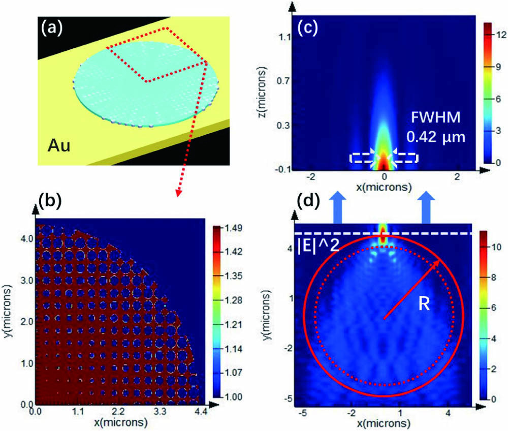
![(a) Schematic diagram for a PMLL. (b) Quarter enlarged view of the top of the dielectric film with air holes. (c) Transverse cross section of the intensity profile at the point ρ=R in the y direction. (d) Intensity distribution of SPPs [three-dimensional (3D) simulation] propagating along y direction and passing through a PMLL. The red circle indicates the radius R of the PMLL. The red dotted circle indicates the real area of the designed lens. The white dotted line indicates the position y=R.](/Images/icon/loading.gif)
Figure 1.(a) Schematic diagram for a PMLL. (b) Quarter enlarged view of the top of the dielectric film with air holes. (c) Transverse cross section of the intensity profile at the point in the direction. (d) Intensity distribution of SPPs [three-dimensional (3D) simulation] propagating along direction and passing through a PMLL. The red circle indicates the radius R of the PMLL. The red dotted circle indicates the real area of the designed lens. The white dotted line indicates the position .
The index distribution of a traditional Luneburg lens satisfies the expression where characterizes the distance to the center of the PMLL. is the radius of the PMLL. The red circle in Fig. 1(d) stands for the radius R of PMLL. Equation (1) shows that the index profile with a maximum contrast of should be created. Plasmonic dispersion equations of the metal/dielectric/air multilayer model are[22]
Here, is the height of the dielectric film. represents the SPP wave vector along the direction. is the frequency of the SPPs. is the speed of light in vacuum. stands for the permittivity of the air. stands for the permittivity of the dielectric. stands for the permittivity of the Au. The effective mode index of the SPPs can be defined as Eq. (4). It has been proposed that the required effective mode index profile can be realized by varying the height of the dielectric film according to Eqs. (2)–(4). The height of the dielectric film varied in the range of 0–220 nm so that the can vary in the range of 1.02–1.424.
Furthermore, according to Eqs. (2)–(4), this Letter proposed that the required effective mode index profile can also be realized by varying the permittivity of the dielectric . The model can be seen as an Au/220 nm dielectric with changeable permittivity/air multilayer. The changeable permittivity of the dielectric was realized by varying the volume fraction of the air holes in the dielectric film. The period of the air holes array is , which is smaller () than the wavelength . Therefore, the dielectric with air holes can be seen as a new material, which has an equivalent permittivity . The effective medium approximations (EMAs) and volume averaging theory[23] can be used to calculate the equivalent permittivity of the dielectric with air holes:
Here, is the volume fraction of the air hole. The radius of air holes is calculated from the equation . Considering that it is hard for the diameter to be larger than in the manufacturing process, the diameter is set to be 8.7 μm. The red dotted circle in Fig. 1(d) indicates the real area of the designed lens.
The Lumerical FDTD Solutions ® software is used to confirm the design. SPPs propagate along direction and pass through a PMLL [Figs. 1(c) and 1(d)]. The simulation indicated that SPPs focus well at the expected position . The FWHM is 0.42 μm. The focus efficiency is 78%, which shows there is a 22% loss. This loss consists of scattering loss and propagation loss. The primary loss for SPPs is the propagation loss due to the absorption of metals. Compared to the method that varies the height of the PMMA layer on top of a gold substrate, additional scattering loss is small. This also indicates that the approximation (regarding dielectric film with air holes as a uniform material) is relatively accurate. To assess the mismatch caused by manufacturing errors, perturbations were added to the input parameters in the simulations.
The height of the dielectric film is changed to be 170 nm, 200 nm, 250 nm, and 290 nm, while the distribution of air holes has not been changed. The height of air holes is equal to the height of the dielectric film. The simulations shown in Fig. 2 indicate that the location of the focus point is stable () when the height of the dielectric film is changing within the range of 170 nm to 290 nm (220 nm is the designed height). The location of the focus point has a trend toward outside of the PMLL with a decrease of the height of the dielectric film.
Figure 2.(a), (c), (e), and (g) Transverse cross sections of the intensity profile at the point in the direction. (b), (d), (f), and (h) Intensity distributions of SPPs (3D simulation) propagating along direction and passing through the PMLL with different heights. The red circles indicate the radius R of the PMLL. The red dotted circles indicate the real area of the designed lens. The white dotted lines indicate the position .
The radius of the air holes is set to be 90 % or 110 % of the designed values, as shown in Figs. 3(b) and 3(f). The height of the dielectric film stays at 220 nm. The height of air holes is equal to the height of the dielectric film. The simulations shown in Fig. 3 indicate that the location of the focus point is also stable when the radius of air holes is changing to be 90% or 110% of the designed values. Small deviations from the designed values of the radius of the holes will not strongly modify the characteristics of the PMLL. This is consistent with the theoretical analysis. According to the effective medium theory, the effect of manufacturing errors would cause the effective refractive index errors, and the unexpected refractive index distribution would affect the focusing ability. For example, when the height of the dielectric film increases 20 nm, calculated by the plasmonic dispersion equations, the maximum effective refractive index will change from 1.424 to 1.435. The change rate is only 0.7%. Small manufacturing errors will not have a strong effect on the effective index distribution.
Figure 3.(a) and (e) Schematic diagram for a PMLL. (b) and (f) Quarter enlarged view of the top of the PMMA film with air holes. (c) and (g) Transverse cross section of the intensity profile at the point in the direction. (d) and (h) Intensity distributions of SPPs (3D simulation) propagating along direction and passing through a PMLL. The red circles indicate the radius R of the PMLL. The red dotted circles indicate the real area of the designed lens. The white dotted lines indicate the position .
The different length scales limit the integrated optical and electronic devices in a single chip[24]. To associate with photonics and electronics in a single nanoscale device, SPPs should be coupled to a nanoscale waveguide. In view of the excellent focusing ability and the robustness to manufacturing errors, the PMLL can be utilized to design a compact high-performance coupler in photonic and electric integrated circuits, as shown in Fig. 4(b). The input SPP width is set to be 10 μm (it is assumed that the SPPs were excited by an optical fiber using an optical grate), and the output waveguide width was set to 40 nm. The height of the output waveguide is corresponding to the Au substrate.
Figure 4.(a) Schematic diagram for a taper. (b) Schematic diagram for a PMLL coupler. (c) Transverse cross section of the electric field profile at the position . (d) Electric field profile of SPPs propagating along direction, passing through a taper coupler, and coupled to the 40 nm wide waveguide. (e) Transverse cross section of the electric field profile at the position . (f) Electric field profile of SPPs propagating along direction, passing through a PMLL, and coupled to the 40 nm wide waveguide. The red circle indicates the position of the PMLL, and the white dotted line indicates the position of the monitor.
As shown in Fig. 4(b), the PMLL was placed in front of the output waveguide, and the focused SPPs were coupled into the output waveguide after propagating through a PMLL. The taper coupler was used to solve the problem of scale mismatch, and it is widely used in photonic integrated circuits. The taper coupler model was simulated as a standard comparison. The taper coupler has a length of 10 μm ( direction), an input side width of 10 μm, and an output side width of 40 nm, and the coupler width is gradually changing. The simulations show the electric field profile of SPPs propagating along direction and passing through a taper/PMLL [Figs. 4(d) and 4(f)]. The taper coupler shows that the SPPs were not focused, and most SPPs were scattering to the free space. The PMLL coupler shows a higher electric intensity at the point where the SPPs were coupled to the output waveguide. SPPs were well coupled to the output waveguide. It can also be inferred from the cross section of the electric field profile [Figs. 4(c) and 4(e)] that the PMLL coupler performed better [the maximum electric intensity in Fig. 4(c) is 1.7, and the maximum electric intensity in Fig. 4(e) is 4.3].
The calculated coupling loss of the PMLL coupler was 8 dB for the designed wavelength . The calculated coupling loss of the taper coupler was 12.2 dB. In addition, the designed PMLL coupler showed a higher coupling efficiency in a broad bandwidth of , as shown in Fig. 5.
Figure 5.The performance of the PMLL coupler and taper coupler based on 3D simulations in a broad bandwidth.
In conclusion, we demonstrated that a PMLL designed by average permittivity approximation and plasmonic dispersion equations performed well. The characteristics of a PMLL have robustness to manufacturing errors. We also demonstrated that a PMLL can work as a compact coupler in plasmonic integrated circuits; the performance of this kind coupler is far better than the traditional inverse width tapers. Such an element can be manufactured in a single lithographic patterning step, which means such elements have great potential to be widely used in plasmonic integrated circuits. Furthermore, this method can be used to design plasmonic elements working in the telecom wavelength of 1550 nm. Silicon can be an option of the material of dielectric layer. It shows the potential to integrate electronic, photonic, and SPPs in a single chip. We believe that this design could lead to more feasible and convenient strategies for the production of other GRIN (lens based on GRIN) plasmonic devices.
References
[1] K. Liu, Q. Wei, Y. Huang, X. Duan, Q. Wang, X. Ren, S. Cai. Chin. Opt. Lett., 17, 041301(2019).
[2] L. Zhou, X. Wang, L. Lu, J. Chen. Chin. Opt. Lett., 16, 101301(2018).
[3] W. L. Barnes, A. Dereux, T. W. Ebbesen. Nature, 424, 824(2003).
[4] A. Maradudin, J. R. Sambles, W. L. Barnes. Modern Plasmonics(2014).
[5] A. Andryieuski, V. A. Zenin, R. Malureanu, V. S. Volkov, S. I. Bozhevolnyi, A. V. Lavrinenko. Nano Lett., 14, 3925(2014).
[6] A. Hohenau, J. R. Krenn, A. L. Stepanov, A. Drezet, H. Ditlbacher, B. Steinberger, A. Leitner, F. R. Aussenegg. Opt. Lett., 30, 893(2005).
[7] S. I. Bozhevolnyi, V. S. Volkov, E. Devaux, J.-Y. Laluet, T. W. Ebbesen. Nature, 440, 508(2006).
[8] S. I. Bozhevolnyi, J. Erland, K. Leosson, P. M. W. Skovgaard, J. M. Hvam. Phys. Rev. Lett., 86, 3008(2001).
[9] H. Ditlbacher, J. R. Krenn, G. Schider, A. Leitner, F. R. Aussenegg. Appl. Phys. Lett., 81, 1762(2002).
[10] P. A. Huidobro, M. L. Nesterov, L. Martín-Moreno, F. J. García-Vidal. Nano Lett., 10, 1985(2010).
[11] J. Renger, M. Kadic, G. Dupont, S. S. Aćimović, S. Guenneau, R. Quidant, S. Enoch. Opt. Express, 18, 15757(2010).
[12] C. T. Tai. Nature, 182, 1600(1958).
[13] J. E. Eaton. IRE Trans. Antennas Propag., PGAP-4, 66(1952).
[14] R. Luneburg. Mathematical Theory of Optics(1944).
[15] J. E. Gómez-Correa, S. E. Balderas-Mata, B. K. Pierscionek, S. Chávez-Cerda. Opt. Lett., 40, 3990(2015).
[16] A. Demetriadou, Y. Hao. Opt. Express, 19, 19925(2011).
[17] C. H. Walter. IRE Trans. Antennas Propag., 8, 508(1960).
[18] J. A. Dockrey, M. J. Lockyear, S. J. Berry, S. A. R. Horsley, J. R. Sambles, A. P. Hibbins. Phys. Rev. B, 87, 125137(2013).
[19] H. Chen, C. T. Chan, P. Sheng. Nat. Mater., 9, 387(2010).
[20] T. Zentgraf, Y. Liu, M. H. Mikkelsen, J. Valentine, X. Zhang. Nat. Nanotechnol., 6, 151(2011).
[21] C. E. Garcia-Ortiz, R. Cortes, J. E. Gomez-Correa, E. Pisano, J. Fiutowski, D. A. Garcia, V. Ruiz-Cortes, H.-G. Cortes, H.-G. Rubahn, V. Coello. Photon. Res., 7, 1112(2019).
[22] Y. Liu, T. Zentgraf, G. Bartal, X. Zhang. Nano Lett., 10, 1991(2010).
[23] S. Li, Z. Zhang, J. Wang, X. He. Opt. Express, 22, 25455(2014).
[24] B. Bai, L. Pei, J. Zheng, T. Ning, J. Li. Chin. Opt. Lett., 18, 041301(2020).