
Fangyuan Meng, Hongyan Yu, Xuliang Zhou, Yajie Li, Mengqi Wang, Wenyu Yang, Weixi Chen, Yejin Zhang, Jiaoqing Pan. Quantum wells micro-ring resonator laser emitting at 1746 nm for gas sensing[J]. Chinese Optics Letters, 2021, 19(4): 041406
- Chinese Optics Letters
- Vol. 19, Issue 4, 041406 (2021)
Abstract
1. Introduction
Accurate measurement of gas components, concentrations, and other parameters plays an important role in many fields. The spectroscopic method, based on the principle of absorption, emission, and scattering of light by gas molecules, with the advantages of non-contact, rapid response, and high selectivity, meeting the requirements of gas measurement under different environmental conditions, is an efficient way for gas sensing[
Nowadays, most semiconductor lasers used for gas sensing are distributed feed-back (DFB) lasers and distributed Bragg reflector (DBR) lasers. However, power consumption and volumes of DFB and DBR lasers are hard to reduce any more, which adversely affect cost reduction and device miniaturization. The microcavity laser with low power consumption and small volume was expected to replace them as a suitable light source. Microcavities can be divided into three types, which are the Fabry–Perot (FP) microcavity, photonic crystal (PC) microcavity, and whispering-gallery (WG) microcavity[
In this Letter, a micro-ring resonator laser used for gas sensing is experimentally demonstrated. The laser consists of a resonator with a 15 µm outer radius, 8 µm inner radius, and output waveguide of 3 µm in width. Single-mode lasing was obtained, for the first time, to the best of our knowledge, at about 1746.4 nm at 288 K. The maximum output power is 1.65 mW with a side-mode suppression ratio (SMSR) over 33 dB.
Sign up for Chinese Optics Letters TOC. Get the latest issue of Chinese Optics Letters delivered right to you!Sign up now
2. Simulation and Calculation
The simulation of the micro-ring resonator laser was based on the finite element method (FEM), which uses a variation of Maxwell equations as the characteristic equations. For example, the characteristic equation of the transverse electric (TE) mode can be described by[
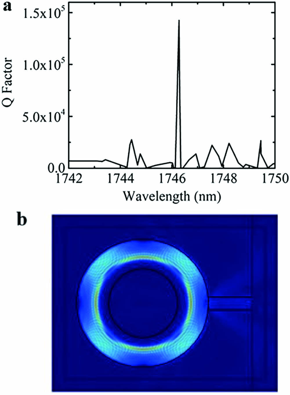
To forecast the factor and mode field distribution of the device, we simulated a micro-ring resonator laser with a 15 µm outer radius, 8 µm inner radius resonator, and a 3 µm wide output waveguide by the two-dimensional (2D) FEM method. The micro-ring resonator and output waveguide with refractive index of 3.2 are confined by air instead of the insulating layer and the p-electrode layer, as in real devices, which has a refractive index of 1.54. Simulation result of the Q value varying with different wavelengths is plotted in Fig. 1(a). A single mode emitting at 1746.3 nm is obtained with a higher-Q factor of . Figure 1(b) shows the mode field distribution of 1746.3 nm.
![]()
Figure 1.(a) Simulation result of the quality factor (Q). (b) Electric field distribution.
3. Fabrication
The fabrication process of the micro-ring resonator laser includes materials epitaxy, photolithography, dry etching, wet etching, metal sputtering, etc. All of these processes can be summarized into two steps, which are materials epitaxy and manufacturing process.
Materials of the laser were grown by metal organic chemical vapor deposition (MOCVD) equipment. Table 1 shows the epitaxial structure of the laser. The whole structure was grown on an InP substrate. Referring to the previous research of semiconductor lasers emitting at 1.7–1.8 µm[
![]()
Figure 2.Optical gain of the QW structure varying with wavelength and carrier concentration Nn.
| No. | Item Name | Thickness (nm) | Doping |
|---|---|---|---|
| 0 | N-InP (Substrate) | / | Si |
| 1 | N-InP (Buffer) | 750 | Si |
| 2 | 1.3 Q InGaAsP (Lower SCH) | 120 | / |
| 3 | Active area (MQWs) | QW: | / |
| 4 | 1.3 Q InGaAsP (Upper SCH) | 120 | / |
| 5 | P-InP (Cladding) | 1700 | Zn |
| 6 | P-InGaAs (Contact) | 200 | Zn |
Table 1. Epitaxial Structure of the Laser
Etching high-Q resonators with a vertical and smooth sidewall plays the core role in the whole production process of the device. Since the wet etching method always has directional selectivity and will lead to a lateral etching, the microcavity was etched by the inductively coupled plasma (ICP) etching method. As a hard mask for etching, 500 nm was deposited by plasma-enhanced chemical-vapor deposition (PECVD) on the InGaAs contact layer. The micro-ring resonator and a short output waveguide pattern were transferred onto the layer using standard photolithography and ICP etching techniques. Under the cover of a mask, the underlying material was etched by ICP as well. To reduce optical absorption losses and ensure lasing Q, the etching depth needs to be about 4.5 µm. The cross-sectional view scanning electron microscope (SEM) image of the etching result is shown in Fig. 3(a). After ICP etching, the next significant production process is electrode preparation. To efficiently pump the WGM region, the electrode contact is just over the resonator. A Ti–Au p electrode layer was formed over the wafer by magnetron sputtering, and the electrode pattern was defined by wet etching. The wafer was thinned down to 150 µm, and an Au–Ge–Ni–Au later was formed as an n-type contact on the back of the InP substrate by metal evaporation. After rapid thermal annealing, the device was completed. Figure 3(b) shows the top-view SEM image of the finished device.
4. Experimental Results and Discussion
The laser was tested on a thermoelectric cooler (TEC), and the temperature was controlled at 288 K. Light power and voltage versus the injection current (PIV) were collected by an integrating sphere, and the PIV curves under 40 mA are plotted in Fig. 4. The light power can come up to about 1.65 mW when the injection current was 40 mA, as shown in Fig. 4. But, the threshold current of the laser cannot be confirmed through these PIV curves. Because of the small laser volume, the spontaneous emission rate is high; almost all of the spontaneous emissions are coupled to the single lasing mode. In addition, due to the high value of the Q factor, most of the spontaneous emission light is confined in the microcavity, resulting in a high intensity. Therefore, the power-current curve does not have an inflection point, so the threshold current cannot be confirmed[
![]()
Figure 3.(a) Cross-sectional view SEM image of the etched ring. (b) Top-view SEM image of the device with a metal electrode, a micro-ring resonator, and an output waveguide.
The lasing spectra were measured by an optical spectrum analyzer with a resolution of 0.05 nm. Light lasing from the device was partially coupled into a tapered fiber and transmitted to the optical spectrum analyzer through a multimode optical fiber. The lasing spectrum at an injection current of 40 mA is shown in Fig. 5. As the figure shows, the central wavelength is 1746.4 nm with SMSR of 33.33 dB. Obviously, only fundamental transverse mode lasing is achieved because the high-order transverse modes are completely suppressed by the ring resonator. To characterize the stability of the device, the spectra under different inject currents were tested. When the injection current varies from 20 mA to 50 mA, with an interval of 10 mA, the central wavelengths are 1745.18 nm, 1745.73 nm, 1746.37 nm, and 1747.07 nm, with the SMSR of 19.30 dB, 31.93 dB, 33.33 dB, and 25.09 dB, respectively, as shown in Fig. 5. The change is 0.063 nm per milliampere as calculated.
![]()
Figure 4.Output power and applied voltage versus the injection current for a micro-ring resonator laser.
![]()
Figure 5.Lasing spectrogram for the micro-ring resonator laser at an injection current of 40 mA.
Compared with DFB and DBR lasers[
5. Conclusion
In conclusion, a WGM micro-ring resonator laser used for gas sensing is experimentally demonstrated. The laser is based on multi-InGaAs/InGaAsP-QWs and an InP substrate. It consists of a resonator with a 15 µm outer radius and 8 µm inner radius, and a 3 µm wide output waveguide. The maximum output power is 1.65 mW at 288 K, as shown in the PIV curve. The lasing spectrum shows that a single-mode lasing was obtained, for the first time, to the best of our knowledge, at about 1746.4 nm at 288 K, with an SMSR over 33 dB.
Compared with other lasers like DFB and DBR lasers, the WG micro-ring resonator laser has a much smaller volume and much lower threshold current, making it promising in gas sensing.
References
[1] W. Liu, Z. Cui, F. Dong. Optical and spectroscopic techniques for environmental pollution monitoring. Optoelectron. Technol. Inf., 15, 1(2002).
[2] K. J. Vahala. Optical microcavities. Nature, 424, 839(2003).
[7] Z. Z. Shen, Y.-Z. Hao, F.-L. Wang, K. Yang, H. Y. Yu, J.-Q. Pan, Y.-D. Yang, J.-L. Xiao, Y.-Z. HuangConference on Lasers and Electro-Optics. Hybrid square/rhomb-rectangular semiconductor lasers for ethylene detection, JW2A.3(2019).
[9] X. Ma. Investigations on coupled cavity lasers and optically injected microcavity lasers(2017).
[11] B. Niu, H. Yu, L. Yu, D. Zhou, L. Zhao, J. Pan, W. Wang. 1.65 µm three-section distributed Bragg reflective (DBR) laser for CH4 gas sensor. J. Semiconduct., 34, 85550Z(2012).
[12] H. Yu, P. Wang, J. Mi, X. Zhou, J. Pan, H. Wang, L. Xie, W. Wang. 1.8-µm DBR lasers with over 11-nm continous wavelength tuning range for multi-species gas detection. 2017 Asia Communications and Photonics Conference (ACP), 1(2017).

Set citation alerts for the article
Please enter your email address
© Copyright 2018-2021 | Chinese Laser Press. All Rights Reserved 沪ICP备15018463号-20