
Guoxuan Liu, Ning Xu, Huaidong Yang, Qiaofeng Tan, Guofan Jin. Miniaturized structured illumination microscopy with diffractive optics[J]. Photonics Research, 2022, 10(5): 1317
- Photonics Research
- Vol. 10, Issue 5, 1317 (2022)
Abstract
1. INTRODUCTION
Structured illumination microscopy (SIM) is a superresolution technique that provides non-invasive fluorescence imaging with resolution beyond the diffraction limit by shifting the unresolvable high-frequency spectrum to the detectable region in the Fourier domain using periodic illumination [1]. It has become a popular tool for live-cell imaging benefiting from its high imaging speed, moderate illumination intensity, and compatibility with most fluorescence labels [2–4]. The superresolution ability of SIM originates from the periodic pattern used for sample illumination. The resolution of the SIM is determined by the spatial frequency of the illumination patterns and the maximum spatial frequency of the system, and is determined by the average observed emission wavelength and numerical aperture (NA) of the imaging objective lens. Generally, the maximum measured spatial frequency is stretched from to to realize superresolution and because cannot exceed , the ultimate theoretical resolution limit becomes [5,6].
To obtain periodic illumination patterns in SIM, a commonly used method was interference. The interference beams generally came from the different diffraction orders while modulating the incident light using different modulators, including a liquid crystal spatial light modulator [4], digital micro-mirror device (DMD) [7–9], and grating [1,10]. Some studies showed that SIM can be compactable and portable based on interference patterns [11,12]. In addition, various techniques were also proposed to obtain periodic illumination patterns in SIM other than interference. One was projecting the periodic pattern loaded on an LED-illuminated DMD to the sample plane of the microscope [7]. Moreover, spot arrays or multifocus spots were also used in SIM to realize simultaneous 3D imaging [13–17]. However, these existing SIM systems were always bulky and were for research use only. For example, the size of the illumination setup in a commercial Nikon-SIM system is about [18], not suitable for those applications sensitive to the mobility and cost of equipment, such as point-of-care testing [19–21]. Although a SIM method based on a photonic chip was proposed recently with dramatic system compactness [22], only total internal reflection fluorescence SIM imaging can be achieved, which was unfortunately incapable of most intracellular studies. Furthermore, the multifocal phase mask can be used to replace the tube lens of a conventional microscope to establish the miniaturized system, albeit with the diffraction-limited resolution [23].
Actually, diffractive optics is another good choice for obtaining two-dimensional periodic patterns but has not been considered in SIM yet. Benefiting from the flexibility of modulating the phase of beams, phase-only diffractive optical elements (DOEs) have been developed to generate various complex light fields, of which the point spread function (PSF) and spatial frequency can be customized, with the cooperation of a wide range of geometries and corresponding design methods, such as the Toraldo concept [24], analytical method [25,26], and iterative algorithms to realize PSF engineering [27–29]. In addition, spot array generation techniques also have powerful built-in capabilities to enable parallel, i.e., faster imaging [30] and widefield imaging [31]. In SIM, obtaining periodic illumination patterns with a spatial frequency high enough is the key factor to achieve high-resolution imaging. However, DOEs have not been exploited to achieve two-dimensional sinusoidal structured illumination to meet the requirement for SIM with superresolution imaging.
Sign up for Photonics Research TOC. Get the latest issue of Photonics Research delivered right to you!Sign up now
Here, we proposed a SIM method assisted with diffractive optics, named miniaturized SIM (Mini SIM). An optimized phase-only DOE was applied to generate a two-dimensional sinusoidal pattern for structured illumination. The employment of the DOE substantially miniaturized the illumination system of Mini SIM to , which was about 2 orders of magnitude smaller than that of the existing commercial SIM [18], while the maximum incident light efficiency can reach 84% in theory. We built up a Mini SIM prototype that used the DOE to generate a sinusoidal spot array () to demonstrate the lateral resolution beyond the diffraction limit. In a superresolution image of fluorescence beads, the average size of a single bead was , while the size in the widefield image was . Superresolution imaging of A549 (adenocarcinomic human alveolar basal epithelial) cells also showed obvious resolution enhancement by resolving adjacent tubulins which were 419 nm apart while the theoretical diffraction-limited resolution was about 630 nm.
2. MINI SIM SYSTEM
The optical configuration of the Mini SIM prototype is demonstrated in Fig. 1, consisting of an illumination system and an imaging system.
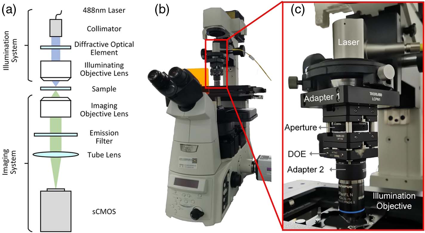
Figure 1.Mini SIM prototype. (a) Optical diagram of Mini SIM. (b) The whole Mini SIM system consists of an illumination system and an imaging system. (c) The miniaturized illumination system of the Mini SIM system, which is installed on the pillar of the microscope.
In the illumination system, the 488 nm laser beam coupled into a single-mode fiber is collimated and expanded with a reflective fiber collimator (RC12FC-P01, Thorlabs). After being modulated by the DOE, the laser beam passes through the illuminating objective lens and the diffraction field forms a two-dimensional sinusoidal pattern for illumination of the sample, owing to the Fourier transform realized by the illuminating objective lens. Thus, the DOE can be mounted on the illuminating objective lens, greatly reducing the size of the illumination system to . In contrast with that of conventional SIM where the modulated plane was generally conjugated with the sample plane, this illumination system of Mini SIM is substantially simplified and miniaturized, as the system consists of only a few components mounted closely.
The imaging system for raw data capturing in the Mini SIM prototype is a commercial microscope (Ti-E eclipse, Nikon). An imaging objective lens is used for emission light collection and an emission filter (ZET 488/561m, Chroma) is used for filtering out the 488 nm illumination (Sapphire 488, Coherent). To acquire higher spatial frequency of structured illumination, we used an illuminating objective lens (, Olympus) with a higher NA than that of an imaging objective lens (, Nikon).
The sample is scanned to nine () different positions using the motorized microscopic stage and controller, and then the raw images, i.e., the structured illuminated sample images, are captured with an sCMOS (Zyla 4.2 Plus, Andor) (see
3. DOE DESIGN
Of particular interest for this Mini SIM prototype is the design of the DOEs that delivers diffractive sinusoidal illumination. The resolution of Mini SIM is determined by the spatial frequency of the two-dimensional sinusoidal spot array and the maximum spatial frequency of the system. Here, we proposed a practical method to design the DOE that generates two-dimensional sinusoidal structured illumination. With that, the DOE was fabricated on a substrate with masks and an etching process to generate the required spot arrays, enabling the illumination quality for the miniaturized SIM prototype in practice.
A. Custom-Made Method for Designing DOEs
Calculating the phase distribution of the DOE that generated the desired diffraction field is essentially a phase retrieval problem. A popular solving method to this problem is the Gerchberg–Saxton (G-S) algorithm owing to its flexibility [33]. Here, we proposed a modified G-S algorithm to design the DOE in Mini SIM.
The procedure of this modified G-S algorithm is depicted in Fig. 2(a), consisting of the following main steps.
For insurances of accurate description of the target field, convergence speed enhancement, and obtaining high-quality iteration result, we made special modifications in the proposed algorithm, which are explained in detail below.
![]()
Figure 2.Process flow to produce a DOE illumination. (a) Flowchart of the modified G-S algorithm for calculating phase distribution of DOEs to realize two-dimensional sinusoidal illumination. The black arrows and the red dotted arrows indicate the iteration and the initial phase calculation, respectively.
The desired two-dimensional illumination pattern, i.e., the square of the target amplitude field of DOE, is
We further modified the G-S algorithm with a more suitable constraint by the desired field amplitude. The light field distribution in the focal plane can be expressed as
B. Verification for DOE Design
In Mini SIM, the FOV is determined by the number of spots generated by the DOE. With the FOV getting larger, the quality of the spot array will be increasingly affected. To obtain a large FOV with high performance, we generate a sinusoidal spot array ( as the illumination pattern in the numerical simulations, adopting 488 nm of the incident wavelength, 0.50 of the NA of the imaging objective lens, 500 of the iteration number, and . The phase distribution of the DOE is shown in Fig. 2(b2). Figures 3(a) and 3(b) are respectively the numerical simulation and experimental result of the spot array, with the inset showing a magnified view of the spot array. It can be seen from Fig. 3 that there are differences of intensity variation between simulation results and experimental results; however, the period of the spot array is not influenced. The period ( of the sinusoidal spot array is 990 nm. The efficiency of the spot array generated by the DOE can be achieved to 61%, which is higher than that of the DMD or projection because all orders generated by the DOE are adopted to generate the spot array rather than some certain orders. The generated spot array deviates from the standard sinusoidal distribution also because all orders generated by the DOE are adopted.
![]()
Figure 3.Verification for DOE design. (a) and (b) are the numerical simulation and experimental result of the
To establish the illumination system of Mini SIM, we fabricated an eight-step DOE by three masks and an etching process with the pixel size of 5 μm and the detailed fabrication is presented in Appendix B. The diameter of the DOE is corresponding to the entrance pupil of the illuminating objective 5 mm, and the optical micrograph of the fabricated DOE is shown in Fig. 2(b3), with the inset showing a magnified view of the center of the DOE. Notably, the diameter of the DOE should be matched with the entrance pupil to make full use of the NA of the illuminating objective lens. There is a distance between the DOE and the entrance pupil of the illuminating objective due to the fixation and assembly requirement, which is about 23 mm in Mini SIM. Although different distances will introduce different spherical phase factor, the analysis shows that the system has a large enough tolerance to the distance. When the distance is , the intensity distribution in the focal plane has no obvious variation, as shown in Fig. 4. Another significant factor for sinusoidal spot arrays is almost without spatial zeroth order, which was realized by the mature high-precision fabrication in the Institute of Semiconductors at the Chinese Academy of Sciences, as shown in Fig. 2(b4).
![]()
Figure 4.Influence of intensity distribution in the focal plane with different distances between the DOE and entrance pupil of the illuminating objective.
The designing and fabricating process of the DOE will possibly induce error between the ideal illumination pattern and the practical diffraction pattern, as shown in Fig. 3. This could result in potential artifact if using the conventional SIM reconstruction algorithm that separates the spectrum components with a phase-determined coefficient matrix. Thus, in Mini SIM, we used an iterative SIM reconstruction algorithm [32] that is more robust to illumination pattern errors. The detailed reconstruction algorithm is presented in Appendix A.
4. EXPERIMENTAL RESULTS
A. Superresolution Imaging of Fluorescence Beads
To quantitatively testify the superresolution capability of the Mini SIM prototype, we performed imaging of fluorescence beads. In this experiment, the theoretical diffraction-limited resolution was 632 nm, which was determined by the numerical aperture of the imaging objective lens (, Nikon) and the emission wavelength of the fluorescence label (Ex488/Em518, Lumisphere). Notably, the illumination path is switched between the widefield and Mini SIM. The widefield resolution is determined by the NA of the imaging objective while the Mini SIM is decided by the spatial frequency of the spot array and the NA of the imaging objective. As the 100 nm diameter of the fluorescence bead was negligible compared with the diffraction-limited resolution, the size of a single bead can be considered as the resolution of an image. Figure 5 demonstrates obvious resolution enhancement by comparing the widefield image of the beads with the Mini SIM image. According to statistic data of 10 different single beads, the average size of a single bead in Mini SIM image was reduced to while in the widefield image it was . The 633 nm size of the beads in the widefield image met the 632 nm theoretical diffraction-limited resolution well, and the much narrower 396 nm size in the Mini SIM image proved that superresolution imaging was achieved. The enlarged images of region of interest (ROI) indicated that two adjacent fluorescence beads with a central distance of 567 nm can be resolved in the Mini SIM image, while in the widefield image, they were blurred and unresolvable, also proving the superresolution capability of Mini SIM.
![]()
Figure 5.Imaging results of fluorescence beads. (a) Widefield image of fluorescence beads and enlarged ROI (lower right) in the boxed region. (b) Mini SIM image of fluorescence beads and enlarged ROI (lower right) in the boxed region. (c) Intensity profiles of fluorescence beads on the selected line in (a) and (b). Scale bar,
B. Superresolution Imaging of Fixed Cells
We also performed superresolution imaging of A549 cells using the Mini SIM prototype to demonstrate the capability of Mini SIM in biological imaging. In this experiment, the tubulins of the A549 cells were labeled with Alexa 488 (Ex505 nm/Em512 nm, Invitrogen) by the thickness of the cell side 1 mm and cover slide 0.17 mm on both sides, and the corresponding diffraction-limited resolution was 625 nm, determined by the 0.5 NA of the objective lens and 512 nm emission wavelength of the fluorescence label. According to the results, the Mini SIM image showed better resolution compared with the widefield image. Abundant proof of resolution enhancement can be found [see Figs. 6(a) and 6(b), lower right], where adjacent tubulins were resolved in the Mini SIM image and were mistaken for thick branches in the widefield image. The Fourier spectrum of the Mini SIM image was expanded compared with that of the widefield image [see Figs. 6(a) and 6(b), upper right], which also proved the enhancement of resolution. For quantitative analysis, intensity profiles of both the Mini SIM and widefield images along the selected line are plotted in Fig. 6(c). Gaussian fitting indicated that the Mini SIM prototype was capable of resolving adjacent tubulins with 419 nm distance between their centers, demonstrating resolving power beyond the 625 nm theoretical diffraction-limited resolution.
![]()
Figure 6.Imaging results of tubulins of A549 cells. (a) Widefield image of tubulins, enlarged ROI (lower right) in the boxed region, and Fourier spectrum (upper right) of the widefield image. (b) Mini SIM image of tubulins, enlarged ROI (lower right) in the boxed region, and Fourier spectrum (upper right) of the Mini SIM image. (c) Intensity profiles of tubulins on the selected line in (a) and (b). Scale bar,
5. DISCUSSION AND CONCLUSION
We developed a Mini SIM superresolution system that used a DOE for two-dimensional periodic illumination for the first time. This diffractive illumination strategy substantially minimized the size of SIM, getting SIM prepared for wider application fields and scenarios. We built up the Mini SIM prototype using a custom-made designed DOE that generated a two-dimensional sinusoidal spot array. Although the two-dimensional periodic spot array is not uniform, superresolution can be achieved through the modified reconstruction algorithm, and further proved the feasibility of Mini SIM by lateral superresolution imaging of fluorescence beads and A549 cell slide.
The Mini SIM prototype is used to verify the validity of the structured illumination realized by the DOE, and the smart phase shifting technique, e.g., the DMD [40] or galvanometer scanning mirror [41], will be used to replace the motorized stage to realize high imaging speed. Here it should be mentioned that the spatial frequency of the illumination pattern is smaller than the maximum spatial frequency of the imaging system, even though the NA of the illuminating objective lens is larger than that of the imaging objective lens. The optimization algorithm should be modified to further increase the spatial frequency and uniformity of the two-dimensional sinusoidal illumination to obtain better performance. It is possible to generate such a spot array with high spatial frequency and good uniformity by the DOE but perhaps sacrificing the FOV [42]. Furthermore, the FOV also can be extended by stitching techniques. The existing Mini SIM prototype focuses on the lateral superresolution imaging, and no axial resolution enhancement is achieved; the axial resolution enhancement may combine with other techniques [23,39] in the future.
The system requires two objectives to realize superresolution imaging at present. It is predictable to develop next-generation Mini SIM by the reflective optical path with a shared objective [43]. Another thing to be mentioned is that, in Mini SIM, the sample should be placed between two cover glasses to satisfy the working condition of the illuminating and imaging objective lenses on both sides. Future optimized design of the sample holder on the stage will provide better support and avoid the potential instable problem in future imaging using oil immersion objective lens.
In summary, the proposed Mini SIM may benefit the applications in wider fields and scenarios, especially for those applications sensitive to the mobility and the cost of equipment, and it has great prospects for developing ultra-high-resolution imaging suitable for biological or medical use.
Acknowledgment
Acknowledgment. We acknowledge Assistant Professor Lingfeng Pan of Institute of Semiconductors, Chinese Academy of Sciences, for fabricating the designed DOE. We acknowledge Dr. Mingjun Jiang at the Department of Biomedical Engineering, Peking University, China, for her kindness providing the A549 cells sample slide. We also thank Dr. Yinjun Jia at School of Life Sciences, Tsinghua University, China, for his helpful assistance during sample preparation. Our deepest gratitude goes to the editor and anonymous reviewers for their careful work and thoughtful suggestions that have helped us to improve this paper substantially.
APPENDIX A: MINI SIM RECONSTRUCTION
To reconstruct the superresolution image, we applied an iterative reconstruction algorithm originated from the Fourier-ptychographic (FP) SIM method [
![]()
Figure 7.Flow chart of Mini SIM reconstruction procedure.
During data acquisition, a widefield image was captured. We first used this widefield image for estimating the shifting vectors of samples in the Mini SIM raw images. Here, an intensity-based registration [
Then, the iteration started. The widefield image was used as the initial guess of the sample image and a uniform intensity was used as the initial guess of the illumination pattern. In each iteration, the sample image and unknown illumination were calculated similarly to that in FP SIM [
After the estimated sample image converged, we stopped the iteration and obtained a sample image with superresolution.
APPENDIX B: FABRICATION OF THE DOE
For the fabrication of the DOE, the silicon dioxide () with dimensions of was chosen as the substrate. A thin layer of photoresist (AZ6130) with a thickness of 2.3 μm was spun onto the substrate at the speed of 2000 r/min for 20 s, and the design phase distribution of the DOE was fabricated via the reactive ion etching method (STS AOE). Finally, the patterned photoresist was removed by mixing sulfuric acid and hydrogen peroxide in a ratio of 1:1 as a cleaning solution.
The binary structure () of the eight-step DOE was measured during fabrication using a step profiler (Taylor Hobson). As shown in Fig.
![]()
Figure 8.
References
[1] M. G. L. Gustafsson. Surpassing the lateral resolution limit by a factor of two using structured illumination microscopy. J. Microsc., 198, 82-87(2000).
[2] X. Huang, J. Fan, L. Li, H. Liu, R. Wu, Y. Wu, L. Wei, H. Mao, A. Lal, P. Xi, L. Tang, Y. Zhang, Y. Liu, S. Tan, L. Chen. Fast, long-term, super-resolution imaging with Hessian structured illumination microscopy. Nat. Biotechnol., 36, 451-459(2018).
[3] Y. Guo, D. Li, S. Zhang, Y. Yang, J. J. Liu, X. Wang, C. Liu, D. E. Milkie, R. P. Moore, U. S. Tulu, D. P. Kiehart, J. Hu, J. Lippincott-Schwartz, E. Betzig, D. Li. Visualizing intracellular organelle and cytoskeletal interactions at nanoscale resolution on millisecond timescales. Cell, 175, 1430-1442(2018).
[4] A. Markwirth, M. Lachetta, V. Mönkemöller, R. Heintzmann, W. Hübner, T. Huser, M. Müller. Video-rate multi-color structured illumination microscopy with simultaneous real-time reconstruction. Nat. Commun., 10, 4315(2019).
[6] L. Schermelleh, R. Heintzmann, H. Leonhardt. A guide to super-resolution fluorescence microscopy. J. Cell Biol., 190, 165-175(2010).
[7] D. Dan, M. Lei, B. Yao, W. Wang, M. Winterhalder, A. Zumbusch, Y. Qi, L. Xia, S. Yan, Y. Yang, P. Gao, T. Ye, W. Zhao. DMD-based LED-illumination super-resolution and optical sectioning microscopy. Sci. Rep., 3, 1116(2013).
[8] K. Isobe, K. Toda, Q. Song, F. Kannari, H. Kawano, A. Miyawaki, K. Midorikawa. Temporal focusing microscopy combined with three-dimensional structured illumination. J. Appl. Phys., 56, 052501(2017).
[9] Q. Song, K. Isobe, K. Midorikawa, F. Kannari. Resistance to optical distortions in three-dimensional interferometric temporal focusing microscopy. Opt. Commun., 430, 486-496(2019).
[10] K. Inazawa, K. Isobe, T. Ishikawa, K. Namiki, A. Miyawaki, F. Kannari, K. Midorikawa. Enhancement of optical sectioning capability of temporal focusing microscopy by using time multiplexed multi-line focusing. Appl. Phys. Express, 14, 082008(2021).
[11] H. Wang, R. Lachmann, B. Marsikova, R. Heintzmann, B. Diederich. UCsim2: 2D structured illumination microscopy using UC2(2021).
[12] A. Sandmeyer, M. Lachetta, H. Sandmeyer, W. Hübner, T. Huser, M. Müller. DMD-based super-resolution structured illumination microscopy visualizes live cell dynamics at high speed and low cost(2019).
[13] S. Abrahamsson, H. Blom, A. Agostinho, D. C. Jans, A. Jost, M. Müller, L. Nilsson, K. Bernhem, T. J. Lambert, R. Heintzmann, H. Brismar. Multifocus structured illumination microscopy for fast volumetric super-resolution imaging. Biomed. Opt. Express, 8, 4135-4140(2017).
[14] A. G. York, S. H. Parekh, D. Dalle Nogare, R. S. Fischer, K. Temprine, M. Mione, A. B. Chitnis, C. A. Combs, H. Shroff. Resolution doubling in live, multicellular organisms via multifocal structured illumination microscopy. Nat. Methods, 9, 749-754(2012).
[15] S. Abrahamsson, J. Chen, B. Hajj, S. Stallinga, A. Y. Katsov, J. Wisniewski, G. Mizuguchi, P. Soule, F. Mueller, C. Dugast Darzacq, X. Darzacq, C. Wu, C. I. Bargmann, D. A. Agard, M. Dahan, M. G. Gustafsson. Fast multicolor 3D imaging using aberration-corrected multifocus microscopy. Nat. Methods, 10, 60-63(2012).
[16] S. Abrahamsson, R. Ilic, J. Wisniewski, B. Mehl, L. Yu, L. Chen, M. Davanco, L. Oudjedi, J. B. Fiche, B. Hajj, X. Jin, J. Pulupa, C. Cho, M. Mir, M. El Beheiry, X. Darzacq, M. Nollmann, M. Dahan, C. Wu, T. Lionnet, J. A. Liddle, C. I. Bargmann. Multifocus microscopy with precise color multi-phase diffractive optics applied in functional neuronal imaging. Biomed. Opt. Express, 7, 855-869(2016).
[17] S. Abrahamsson, M. McQuilken, S. B. Mehta, A. Verma, J. Larsch, R. Ilic, R. Heintzmann, C. I. Bargmann, A. S. Gladfelter, R. Oldenbourg. Multifocus polarization microscope for 3D polarization imaging of up to 25 focal planes simultaneously. Opt. Express, 23, 7734-7754(2015).
[19] J. Wang. Electrochemical biosensors: towards point-of-care cancer diagnostics. Biosens. Bioelectron., 21, 1887-1892(2006).
[20] M. J. Price, S. Endemann, R. R. Gollapudi, R. Valencia, C. T. Stinis, J. P. Levisay, A. Ernst, N. S. Sawhney, R. A. Schatz, P. S. Teirstein. Prognostic significance of post-clopidogrel platelet reactivity assessed by a point-of-care assay on thrombotic events after drug-eluting stent implantation. Eur. Heart J., 29, 992-1000(2008).
[21] C. D. Chin, V. Linder, S. K. Sia. Commercialization of microfluidic point-of-care diagnostic devices. Lab Chip, 12, 2118-2134(2012).
[22] Ø. I. Helle, F. T. Dullo, M. Lahrberg, J.-C. Tinguely, O. G. Hellesø, B. S. Ahluwalia. Structured illumination microscopy using a photonic chip. Nat. Photonics, 14, 431-438(2020).
[23] K. Yanny, N. Antipa, W. Liberti, S. Dehaeck, K. Monakhova, F. L. Liu, K. Shen, R. Ng, L. Waller. Miniscope3D: optimized single-shot miniature 3D fluorescence microscopy. Light Sci. Appl., 9, 171(2020).
[24] G. T. di Francia. Super-gain antennas and optical resolving power. Nuovo Cimento, 9, 426-435(1952).
[25] P. J. Valle, M. P. Cagigal. Analytic design of multiple-axis, multifocal diffractive lenses. Opt. Lett., 37, 1121-1123(2012).
[26] F. Vega, M. Valentino, F. Rigato, M. S. Millán. Optical design and performance of a trifocal sinusoidal diffractive intraocular lens. Biomed. Opt. Express, 12, 3338-3351(2021).
[27] F. Wyrowski, O. Bryngdahl. Iterative Fourier-transform algorithm applied to computer holography. J. Opt. Soc. Am. A, 5, 1058-1065(1988).
[28] M. Martínez-Corral, L. Muñoz-Escrivá, M. Kowalczyk, T. Cichocki. One-dimensional iterative algorithm for three-dimensional point-spread function engineering. Opt. Lett., 26, 1861-1863(2001).
[29] N. Xu, Z. Kong, Q. Tan, Y. Fu. Multiring pure-phase binary optical elements to extend depth of focus. Appl. Opt., 57, 9643-9648(2018).
[30] L. Sacconi, E. Froner, R. Antolini, M. R. Taghizadeh, A. Choudhury, F. S. Pavone. Multiphoton multifocal microscopy exploiting a diffractive optical element. Opt. Lett., 28, 1918-1920(2003).
[31] Z. Li, M. Taphanel, T. Längle, J. Beyerer. Direct-imaging DOEs for high-NA multi-spot confocal microscopy. tm–Technisches Messen, 87, S40-S43(2020).
[32] S. Dong, P. Nanda, R. Shiradkar, K. Guo, G. Zheng. High-resolution fluorescence imaging via pattern-illuminated Fourier ptychography. Opt. Express, 22, 20856-20870(2014).
[33] R. W. Gerchberg, W. O. Saxton. A practical algorithm for the determination of phase from image and diffraction plane pictures. Optik, 35, 237-250(1971).
[34] J. R. Fienup. Phase retrieval algorithms: a comparison. Appl. Opt., 21, 2758-2769(1982).
[35] W. O. Saxton. Computer Techniques for Image Processing in Electron Microscopy(1987).
[36] Z. Kong, N. Xu, H. Xiao, Q. Tan. Effective Fresnel diffraction field extension of diffractive optical elements with plane wave incidence. Appl. Opt., 59, 3427-3431(2020).
[37] N. Xu, G. Liu, Z. Kong, Q. Tan. Creation of super-resolution hollow beams with long depth of focus using binary optics. Appl. Phys. Express, 13, 012003(2020).
[38] R. Brauer, F. Wyrowski, O. Bryngdahl. Diffusers in digital holography. J. Opt. Soc. Am. A, 8, 572-578(1991).
[39] N. Xu, G. Liu, Y. Zhao, Q. Tan. Ultrahigh-aspect-ratio beam generation with super-resolution spot. Appl. Phys. Lett., 119, 094101(2021).
[40] Q. Geng, C. Gu, J. Cheng, S. Chen. Digital micromirror device-based two-photon microscopy for three-dimensional and random-access imaging. Optica, 4, 674-677(2017).
[41] Y. Choi, C. Yoon, M. Kim, T. D. Yang, C. Fang-Yen, R. R. Dasari, K. J. Lee, W. Choi. Scanner-free and wide-field endoscopic imaging by using a single multimode optical fiber. Phys. Rev. Lett., 109, 203901(2012).
[42] N. Xu, G. Liu, Q. Tan. Adjustable super-resolution microscopy with diffractive spot array illumination. Appl. Phys. Lett., 116, 254103(2020).
[43] Z. Li, M. Taphanel, T. Längle, J. Beyerer. Confocal fluorescence microscopy with high-NA diffractive lens arrays. Appl. Opt., 61, A37-A42(2022).

Set citation alerts for the article
Please enter your email address
© Copyright 2018-2021 | Chinese Laser Press. All Rights Reserved 沪ICP备15018463号-20