A history and a glimpse into the future of spaser (acronym for “surface plasmon amplification by stimulated emission of radiation”) is provided. The spaser (also called a plasmonic nanolaser) is an active nanosystem including a gain medium and a nanoplasmonic metal core. It generates coherent intense nanolocalized fields. Theoretically predicted in 2003 by Bergman and Stockman, the spaser grew into a large fundamental research and application field with thousands of publications. We review a few of them to illustrate the most important and general fundamental properties of the spaser. We also review some selected applications of spasers, in particular, to ultrasensing and biomedical problems, concentrating on cancer-cell theranostics (therapeutics and diagnostics). In conclusion, we attempt to glimpse into the future by predicting that the next big development of the spasers will be topological nano-optics, and its “killer” application will be ultrafast, high-density on-chip communications for future information processing.
This article is devoted to a review of experimental and theoretical studies of optical phenomena in active (i.e., with gain) systems. These systems are spasers and nanolasers,1–77 quantum generators, and amplifiers of local electromagnetic fields on the nanoscale.
The invention of the laser78–80 radically changed science and technology and related fields such as biomedicine and defense. The lasers allow one to concentrate optical energy in space and time or frequency. This allows for coherent beams with a minimum angular divergence or spatial concentration down to a half wavelength. The lasers also allow one to generate the shortest optical pulses with duration on the order of a single optical cycle opening an access to subcycle phenomena.81,82
However, the spatial concentration of the laser-radiation energy is still limited to a half wavelength, due to the wave nature of light. At the same time, there are many important objects and phenomena on the nanoscale that represent a significant fundamental and applied interest, as argued by Feynman.83 Among them are subcellular structures and biological macromolecules that have sizes on the order of 10 nm and such technological marvels as transistors. Therefore, the generation of optical oscillations on the nanoscale has a great significance.
Sign up for Advanced Photonics TOC. Get the latest issue of Advanced Photonics delivered right to you!Sign up now
Obviously, the photons cannot be compressed to sizes much less than the wavelength, , where is the speed of light in vacuum, is the optical frequency, and is the permittivity of the medium. This size is on the order of or greater than a hundred nanometers, which is much greater than our size of interest . Use of plasmonic nanoparticles and tapers to concentrate optical energy due to plasmonic resonance and geometric concentration is a proven approach to nanoscopy, nanospectroscopy, and nanoscale detection and sensing.84–87
2 Fundamentals of Spaser as a Quantum Generator and Amplifier of Nanoscale Optical Fields
2.1 Fundamental Idea of Spaser
The idea of the spaser as a nanosource of optical energy is that the quanta in the laser and photons are not exceptional. General properties of the quanta to satisfy the suitability for a coherent quantum generation are (i) Bose statistics that are necessary to accumulate a significant number of the quanta in a single mode; (ii) high linearity or harmonicity, which provides a possibility to accumulate such quanta and achieve a high field amplitude without a significant nonlinear (anharmonic) frequency shift (chirp) and deterioration of the quality factor of the resonance; (iii) electroneutrality; otherwise, the accumulation of many quanta would cause their Coulomb repulsion and an energy increase , which is unrealistic for .
These properties are inherent in surface plasmons (SPs)—including the localized surface plasmons (LSPs) and the propagating surface plasmon polaritons (SPPs).86 The LSPs can fundamentally possess the strongest localization of any optical quanta88 (see the explanation below).
The modal field potential of an LSP, , satisfies a quasistatic equation,
Here, we assume that the system consists of metal and dielectric; is the characteristic function, in the metal and in the dielectric;88 is an eigenvalue, and is the corresponding eigenfunction. As is appropriate for such an eigenproblem, we assume homogeneous Dirichlet–Neumann boundary conditions. One can readily show that . Equation (1) per se does not possess any spatial scale except for the size of the nanosystem, which is determined by the characteristic function . This implies that the LSPs localize at the nanometric minimum scale of the system.
The LSPs [Eq. (1)] obviously satisfy the above-formulated three requirements: (i) their modal field is a vector, ; consequently, they are spin 1 bosons by the Pauli theorem.89 (ii) The LSPs are electroneutral, as follows from Eq. (1). (iii) The LSPs are found to be highly harmonic due to their nature as collective excitations of many electrons. Similar properties are true for SPP; however, they are propagating waves and, consequently, less localized compared to the LSPs. Also, the SPs interact with electrons via their modal electric fields , similarly to the photons. As a result, the SPs can also be used for quantum amplification/generation. A fundamental advantage of using the SPs instead of photons is their nanoscopic localization size. The SP amplification by stimulated emission of radiation (spaser) has been introduced in Ref. 1, see also Refs. 4, 9, 10, 47, and 90.
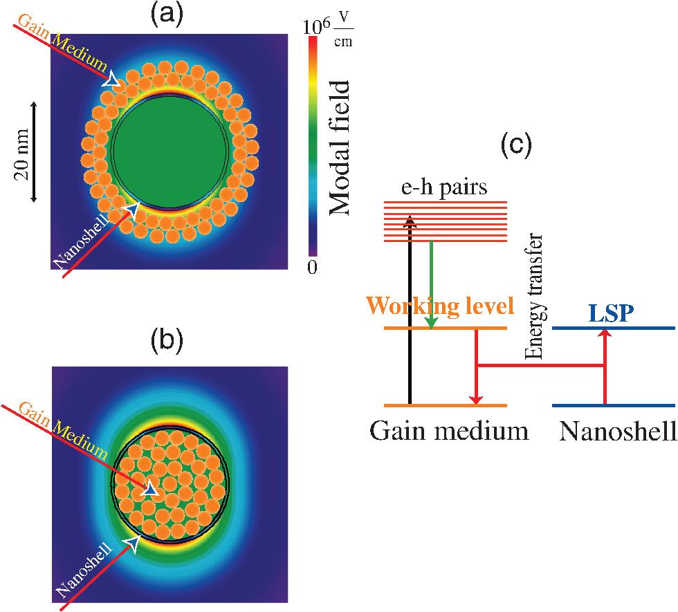
A possible spaser geometry and fundamentals of its functioning are schematically shown in Fig. 1. The gain medium shown in Fig. 1 can be either a nanostructure of a bulk semiconductor, semiconductor quantum dots (QDs), or dye molecules. We will describe them as a semiconductor nanoshell; the cases of QDs and dye molecules are analogous.
Figure 1.Conceptual schematic of a realistic nanospaser geometry, composition, and its action principle. (a) Schematic of geometry and composition of a nanoshell spaser with gain medium outside. The local fields (per one plasmon in a dipolar spasing mode) are shown by color coding by the bar to the right. Plasmonic nanoshell and gain medium (orange dots) are indicated. (b) The same as (a) but for the gain medium inside the shell. (c) Schematic of the spaser functioning. Energy levels of the gain medium are depicted to the left and of the plasmonic core (the nanoshell in this case) are shown to the right. External source (optical or electrical, indicated by a vertical black arrow) injects electrons into the CB creating nonequilibrium (hot) electron–hole plasma. The hot carriers relax to the bandgap (vertical green arrow), possibly forming excitons. These excitations decay without radiation by transferring their energy to LSPs of the nanoshell (shown by coupled red arrows). These SPs stimulate emission of more SPs causing an avalanche of generation eventually stabilized by the saturation of the gain medium. Adapted from Refs. 4 and 57.
A pumping source excited electrons into the conduction band (CB) and holes into the valence band (VB) of the gain medium, causing a population inversion. These relax, forming the inversion at the bandgap (due to the high required free carrier density, excitons would likely be over-screened and dissociate). The transitions in the gain medium are coupled to the LSP-excitation/annihilation [Fig. 1(c), red arrows] by a near-field radiationless coupling term in the Hamiltonian , where is an electronic transition dipole in the gain medium.
A semiquantum theory, which treats the gain medium by quantum-mechanical density matrix equations and the SPs as a classical field, has been given in Ref. 10. A nanospaser has many general unique properties, which are due to its subwavelength size. In such a case, no electromagnetic length (wavelength, skin depth, evanescent decay length, etc.) is important. The theory of the spaser contains only a single important size: a characteristic scale of the metal nanosystem to be denoted as .
2.2 Fundamental Properties Uniquely Inherent in Nanospasers
As presented in the previous section, the spaser has a number of general properties, which make it quite different from those of lasers whose sizes are comparable or exceed the optical wavelength. We discuss these properties below.
2.2.1 Size independence of spasing condition
The spasing condition does not depend on the size of the spaser, as defined by an inequality91where is the bulk density of gain active electrons, and the quality factor of the metal is defined as , where is the metal permittivity at the spasing frequency, is the spectral width of the working transition, and is the dielectric constant of the embedding dielectric. This can be rewritten91 in terms of the bulk linear gain, , of the spaser gain medium; it becomes , where the threshold gain is , and is the light wave vector in the embedding dielectric. For a typical plasmonic metal, ; consequently, the spasing condition is completely realistic to satisfy with semiconductors or dyes as gain media. Since the condition [Eq. (2)] is independent from size , the spaser can be made fully nanoscopic. Also, this condition contradicts a common misconception that the spasing is related to the so-called Purcell effect (enhancement of radiation into a small-cavity mode).92 In actuality, there is no size in Eq. (2) whatsoever. In fact, there have been fully nanoscopic spasers demonstrated,7,29,40 that have very small thresholds—cf. Figs. 3(a) and 3(b).
Shell-geometry spasers are demonstrated, as in Fig. 1(a), with sizes .7,40,58 Such spasers are suitable for unique applications due to their nanometric scales, including the biomedical applications as intracellular labels and theranostic agents, including cancer theranostics (diagnostics and therapeutics)40 and super-resolution imaging by stimulated emission depletion (STED).58
2.2.2 Spasing frequency and the walk-off effect
The spasing frequency, , is an average of the gain transition frequency, , and the LSP frequency, : where is the SP relaxation rate (resonant width). This spasing frequency does not depend on the size or the pumping rate of the spaser. In general, it differs from either the gain-medium transition frequency, , or the SP frequency, . This effect is familiar from the laser physics, where it is called the cavity-pull or frequency-walk-off effect. It is inherent in spasers as well as lasers. Importantly, for the spasers, it can be very large due to large spectral widths involved. In particular, this fact allows one to tune the spasing frequency in a wide spectral range (across the entire visible spectrum) by changing the transition frequency, , of the semiconductor gain medium with the fixed geometry and composition of the metal core,29 see also Fig. 2(e) and its discussion. The peculiarity for the nanospaser frequency, of Eq. (3), depending only on the spaser’s shape and material composition but not on its size, allows for the nanospaser to function as an outstanding frequency-based sensor of the dielectric environment composition. It is also able to detect an extremely small amount of analyte due to its own nanoscopic volume.
2.2.3 Spontaneous decay rate and linear light–light line
The spontaneous decay rate, , of the gain-medium excitation into the LSP spasing mode is plasmonically enhanced. For a nanoshell spaser, it can be expressed as10where and , and is the nanoshell’s external radius. An estimate for silver in the red spectral region and for realistic parameters, , and , results in .10 This rate greatly exceeds those of the competing decay channels in the gain medium. This implies that an excitation of an electron into the gain medium CB causes a spontaneous emission of an SP into the plasmonic core. As a consequence of this, we have a proportionality , where is the plasmon population of the spasing mode, and is the pumping rate. Consequently, the spaser radiation rate, , as a function of the pumping [the so-called L–L (light–light) or L–P (light–pump) curve] is linear even for small , below the spaser threshold. Above this threshold, the emission becomes stimulated, and its rate is increased by a factor of ; however, the L–L curve, , is always a straight line. In such a case, the spasing threshold is invisible in the L–L curve. Because, in Eq. (2), , these “ultralow threshold” or “thresholdless” dynamics are always present for small enough nanospasers with a good spectral overlap between the gain line and the SP mode, such a behavior was demonstrated in many experiments; see, in particular, Ref. 29 and Figs. 3(a) and 3(b).
2.2.4 Relaxation rate and the fundamental limit on direct modulation rate of spaser
Above the spasing threshold, the SP emission becomes stimulated, and its emission rate is expected to increase with pumping intensity as . Note that is also the relaxation rate of a generating spaser. Because the scaling is and [Eq. (4)], the generating spaser relaxation rate, , does not depend on size and is proportional to the pumping rate, . In such a way, the nanospaser can be used for the direct modulation with the frequency of , which is proportional to the pumping rate; it can also be used to generate ultrafast pulses with duration —see theory in Ref. 10. There was experimental evidence that the spaser could be modulated with the rate in excess of , where the pulses generated were shorter than 0.8 ps.32
2.2.5 Shawlow-Townes fundamental limit on linewidth of spaser generation
The spectral width of the spasing line is . The fact that the generating frequency of the spaser is uniquely defined by the spectral parameters [see Eq. (3)] does not indeed imply that the spasing spectral width, , is zero. In fact, analogous to the laser, the width for the spaser is determined by the quantum fluctuations of the field of the generating plasmon mode. According to the Schawlow–Townes theory,79 this width is defined by a spontaneous radiation of incoherent plasmons into the generating coherent mode. These plasmons have random phases, causing the phase diffusion of the coherent plasmon field. In the spectral domain, this implies a broadening of the spectral line.
Figure 2.All-color InGaN@GaN nanorod spasers (plasmonic nanolasers). (a) Schematic diagram of the nanospaser structure: single core–shell nanorods were dispersed on the -covered epitaxial Ag film. The scanning electron microscopy (SEM) image on the upper right indicates that one can measure the laser emissions from individual single nanorods with a collection area of about in diameter using a focused excitation laser beam. (b) All-color, single-mode lasing images observed from single nanorods with an emission line width . (c) The simulated energy density distribution of a blue (474 nm) nanospaser. The resonant field is tightly confined in the 5 nm, low-index () gap layer grown by ALD, and the plasmonic cavity mode is formed between the nanorod and the epitaxial Ag film. (d) Concurrent RGB lasing from three nanorods placed close to each other. The optical pumping source is a 405-nm, CW semiconductor laser diode with an excitation power density of . The scale bar represents . (e) An ultrasmall plasmonic nanolaser (spaser) emitting at 627 nm (red) that is pumped below () and above () the spasing threshold. Both the OM images and the emission spectra show that a strong frequency pulling effect occurs during transition from spontaneous emission (642 nm) to lasing (627 nm). Adapted from Ref. 29.
Figure 3.Spectral and temperature dependence of spasing threshold and line width. (a) Characteristic L–L plots measured from individual RGB nanolasers. The pumping laser polarization direction was chosen to be perpendicular to the rod axis. Here, plots of the emission peak intensity versus the CW pumping intensity (L–L plots) for blue (474 nm), green (554 nm), and red (627 nm) spasers (plasmonic nanolasers) are shown for comparison. The different onsets of kinks in the L–L plots indicate that the lasing thresholds are 140 and , and undetectably small () for red, green, and blue nanolasers, respectively. The fitted spontaneous emission coupling factors () of RGB nanolasers are found to be (red), (green), and (blue) using a rate equation model. (b) Temperature-dependent L–L plots showing lasing thresholds at temperatures varied from 7 to 120 K for the blue (474 nm) nanolaser shown in (a), which exhibits an undetectable lasing threshold at 7 K. The inset shows the measured temperature dependence of the lasing threshold. (c) Temperature evolution of the spectral line width for two blue-emitting nanorods measured with and without the plasmonic cavity at varied temperatures from 7 to 300 K. These measurements were performed at a fixed pump intensity of , as shown in (b). The cyan dots represent measurement results for a single InGaN @GaN core–shell nanorod placed directly on a silicon substrate and emitting at 475 nm (RT). The fitted curve exhibits a typical PL line width narrowing behavior. In contrast, the blue dots show the measurement results for the blue (474 nm) nanolaser case with the plasmonic core (cavity), where we discover a characteristic staircase line width narrowing behavior. Three line width regions can be identified that include the lasing region (I; for ), the SP-coupled PL region (II; for temperature ), and the gain-medium PL region (III; ), respectively. (d) To confirm the lasing behavior in the time domain, second-order photon correlation functions were measured under the same pump intensity () at 80 and 7 K, respectively. As shown in (b), the pump intensity is right below the lasing threshold at 80 K. Indeed, is measured to be greater than one, as expected for the case of thermal emission. In comparison, when the pump intensity is above the lasing threshold at 7 K, we confirm that and remains at unity for all , which is an unambiguous signature of nanolasing (spasing), which is due to a rapid recovery of plasmon population after the emission of a quantum. Adapted from Ref. 29.
The Schawlow–Townes formula for the radiation line width, , of a single mode laser is given by Eq. (17) of Ref. 79 as , where is the laser frequency, is the cavity power, for which a laser is the radiated power, and is the spectral width of the gain-medium working (lasing) transition. To adapt it to the case of the spaser, we note that the spaser does not emit an appreciable fraction of the generated energy as light, and, consequently, the power is determined by the losses in the metal, which implies that , where is the number of plasmons in the generating mode. Other quantities translate as , , and . Substituting this, we obtain
Typically, and . Therefore, the spasing spectral width, , is very small: much less than both the spontaneous emission width of the gain medium, , and of the spontaneous plasmon radiation, . Such a narrow spectral line of the spaser, which becomes narrower as the pumping rate increases, , is one of the most important features of the spaser. Note that in accord with theory of Ref. 93, the actual generation spectral width should be two times less than that of Eq. (5), which is not fundamentally important for the purposes of this article.
2.2.6 Spasing threshold and second order autocorrelation function
No visible threshold in the L–L line, or , does not imply that there actually is no threshold for the coherent spasing. A spasing threshold still exists, and it can be found from the second-order autocorrelation function: where is the detection probability for a photon from the spaser at a time , and is the time delay between the detection of two consecutive photons. The normalization is such that for . This and higher-order correlators are often employed to determine the statistics of photons.94
Below the threshold, the local and emitted fields of the spaser possess random statistics. In the extreme Gaussian limit, for (Hanbury Brown–Twiss correlation95). In general, below the threshold, . Immediately above the threshold, the spaser generation statistics change, and, for pumping above the threshold, one expects for all . Such a peculiarity is characteristic for a single-mode laser.94 For a nanospaser, such a behavior has been decisively shown experimentally,18,29 see also Fig. 3(d) and its discussion. Note that this behavior can be viewed as a nonequilibrium phase transition, where the local fields around the spaser become coherent and large, in sharp contrast to the spontaneous SP emission.
3 Experimental Observations of Spasers
3.1 Fundamental Properties of Spasers Using a Nanorod Spaser as an Example
The historically first spaser observed was a nanoshell LSP spaser7 that contained a metal nanosphere as the plasmonic core surrounded by a dielectric shell containing gain material, specifically, dye molecules. Since then, other nanoshell LSP spasers were observed.40,58 Such spasers are the smallest coherent generators produced so far, with sizes on the order of several to tens of nanometers.
Almost simultaneously with the original observation, another type of spasers (nanolasers) was demonstrated8 that were built from a semiconductor gain nanorod placed at a surface of a plasmonic metal. It has a micrometer-scale size along the nanorod and nanometric diameter, and its modes are SPPs with nanometer-scale transverse size. Given that the spasers of this type are relatively efficient sources of far-field light, they are traditionally called nanolasers though an appropriate name would be SPP spasers. A term “nanolaser” has become traditional but it obviously is indeed a misnomer: light cannot be confined and amplified on the nanoscale, in contrast to the SPs. The emission of light by the spasers is a leak of the mode into the surrounding free space, and it plays no role in the functioning of the spasers except that it introduces some extra losses. Later, this nanorod type of nanolasers (SPP spasers) was widely developed and perfected.14,19,30,33,43,51
There are also LSP nanospasers that are similar in design to the SPP nanolasers but are true nanospasers whose dimensions are all on the nanoscale. Such a spaser consists of a monocrystal nanorod of a semiconductor gain material deposited atop a monocrystal nanofilm of a plasmonic metal,18,29 see Figs. 2(a) and 2(e). These spasers may possess very low thresholds or even imperceptible thresholds as Fig. 3(a) demonstrates and are tunable in all visible spectra by changing the gain semiconductor composition while the geometry remains fixed,29,35,66 see Figs. 2(b) and 2(d). Such a tunability is due to the frequency walk-off (cavity-pull) effect [see above Eq. (3) and its discussion], which is strongly pronounced in spasers due to the wide spectral width of the SP resonances and strong feedback related to high modal fields. Note that this effect is pronounced in Fig. 2(e), where spontaneous radiation has a maximum at 642 nm, while the spasing line sharply peaks at 627 nm.
The threshold behavior of this type of spasers is shown in Fig. 3. As one can see from Fig. 3(a), the L–L curves (note the double logarithmic scale) all contain a linear part at low pump intensity, which is due to spontaneous emission into the mode. Then, at higher pumping rates, the green and red spasers’ L–L curve bends up due to the onset of stimulated emission. Finally, above the spasing threshold, the L–L dependence becomes linear again, which is characteristic of the spasing.
Note that the blue spaser does not show any appreciable bending or threshold behavior [Fig. 3(a)]. These peculiarities can be understood if one assumes that the eigenfrequency of the generating SP mode is in the blue spectral range. Then, it is well matched to the transition frequency in the gain medium. In such a case, the dominating mechanism of the gain medium decay is the resonant energy transfer to the SP mode that, consequently, gets all of the energy from the gain medium, which is proportional to the pump intensity.
For the green and red spaser, when the gain-medium transition frequency decreases, the SP modal frequency does not change. This causes the correspondingly increased frequency walk-off (gain-medium pull) and the increased threshold. In this case, only a part of the pump energy is transferred to the SP mode because the active transition rate is diminished and does not dominate over other relaxation processes. When spasing starts, then the transitions become stimulated, and their rate dramatically increases to dominate over spontaneous relaxation. In such a case, all energy is transferred from the gain medium to the spasing SP mode, the intensity of the mode radiation increases, and the L–L curve becomes linear again. Indeed, with an increase of the gain-mode detuning, the increase of the spasing threshold and increase of spasing intensity above the threshold become progressively larger. This is in full qualitative agreement with the green and red curves in Fig. 3(a).
This specific spaser turns out to be temperature sensitive, as the L–L curves in Fig. 3(b) demonstrate. The thresholds appear at temperatures 40 K and above, showing themselves as bends in the L–L curves. For instance, at 40 K, the threshold is at the pumping intensity of . The threshold disappears completely at 120 K, implying that at this temperature and above there is no spasing in this system.
Not only the intensity and frequency of the spasing radiation is of interest but also its the spectral width, which is shown in Fig. 3(c) (blue dots) along with a control—radiation of a similar nanoshell rod but in the absence of the metal (green dots) as a function of temperature at a pumping intensity of , where the spasing takes place for temperatures below 40 K. There is a sharp decrease of the spaser line width in the area denoted as I at a temperature below 40 K, which is characteristic for the onset of spasing, as described in Ref. 10 (such a narrowing of the laser line is known in the physics of lasers as the Schawlow–Townes effect79).
As we have already discussed above in this section, the blue spaser L–L line at 7 K in Figs. 3(a) and 3(b) does not exhibit any threshold. However, this does not imply that the threshold does not exist. It can be revealed by measuring the two-photon correlation function, , as a function of the time delay, , between the two photons, see Eq. (6) and the discussion that follows it. The correspondent measurement for the “thresholdless” blue spaser at a pumping intensity of is shown in Fig. 3(d). Note that at this pumping, the temperature threshold is between 40 and 50 K, see Fig. 3(b). The upper curve is measured at a temperature of 80 K, which is below the threshold (no spasing and coherent SP population is expected). In fact, does exhibit a pronounced maximum at , which implies the random phases of different SP quanta populating the mode. In stark contrast, a similar correlator measured at 7 K, i.e., above the spasing threshold, shows a straight line with absolutely no maximum at . This is a characteristic sign of spasing: after an emission of a photon, the spaser regenerates the stationary SP population within less than 100 fs,10 where time is shorter than the temporal resolution of the photodetector. Consequently, the photodetector sees the same photon flux as before the emission of the first photon, and, consequently, .
3.2 Multitude of Observed Spasers and Their Type Classification
There are also other types of demonstrated spasers. Among them, we mention semiconductor-metal nanolasers,55 SPP spasers with plasmonic waveguide resonators and quantum-dot gain media,70 and QDs on flat metal LSP spacers.61 The observed spasers range in sizes from 20 nm diameter to several micrometers; most of them operate under ambient conditions, though a few require cryogenic conditions. Currently, the multitude of the observed spasers of all types covers a very wide spectral range from infrared13,17,27,46,62–67 to visible7,8,14,19,29–31,38,40,43,44,48,49,51,56,58,68–74 to ultraviolet.32–34,75–77
A fundamentally different type of quantum generators is the lasing spaser introduced in Refs. 5 and 23. Such a spaser is a periodic lattice (plasmonic crystal) of individual spasers that interact in the near field and form a coherent collective mode. Such a lasing spaser is a plasmonic crystal that incorporates a gain medium. One type of lasing spasers is a periodic lattice of holes in a plasmonic metal film deposited on a semiconductor gain medium.27 Another type is a periodic lattice of metal nanoparticles surrounded by a dye molecules solution.64 We have recently proposed a topological lattice spaser that is built of a honeycomb plasmonic crystal of silver nanoshells containing a gain medium inside.60 The generating modes of such a spaser are LSPs with chiral topological charges of . This difference of charges topologically protects them against mixing: only one of the topologically charged modes can be generated at a time selected by a spontaneous breaking of the time-reversal () symmetry.
A distinct type of topological spaser recently proposed is a plasmonic metal nanodisk positioned over a shape-matching nanopatch of a two-dimensional semiconductor (transition metal dichalcogenide).59 Pumped with circularly polarized radiation, this spaser generates a chiral mode whose local fields corotate in time and space around the metal nanodisk.
A majority of the proposed and observed nanospasers1–77 can be classified into three classes according to the dimensionality of the nanoconfinement of the local optical fields.
3.3 Demonstrated and Potential Application of Spasers
There is a large number of potential applications on spasers based on their properties as sources of intense coherent nanolocalized optical fields. Among those realistically demonstrated, we mention applications to sensing and detection,30,43,44 which are fundamentally based on the above-mentioned fact that the spasing frequency depends on geometry and composition of the spaser [see Eq. (3)] and rather weakly, if at all, depends on the pumping and the ambient temperature. A shift of the spaser indicates change of the close nano-environment of the spaser, which is caused by the presence of the analyte.
One type of such detectors30 is a nanoslab (600 nm length and 50 nm thickness) of CdS deposited on a silver surface and separated from it by a nanofilm (8 nm thick), see Figs. 4(a) and 4(b). This system is an SPP nanospaser with a one-dimensional confinement pump optically. The assumed mechanism of its functioning as a microsensor is shown in Fig. 4(a), where the gain crystal of is also a chemical sensor: the analyte molecules bind to its surface passivating the defects, which causes an increase of the spaser radiation intensity without changing its frequency. An advantage of such a microsensor is small detection volume and a high sensitivity to the analyte binding. The functioning of this sensor is shown in Fig. 4(c), where the introduction of vapors of an explosive chemical analog, 2,4-dinitrotoluene (DNT), in the concentration of 8 parts per billion (ppb) causes an increase of the output intensity by without shifting its spectral maximum. The stability, reproducibility, and sensitivity of this sensor down to 1 ppb are shown in Fig. 4(d).
Figure 4.(a) Sensing is based on the intensity change in stimulated emission from an SPP nanolaser with subwavelength electromagnetic field confinement, where the semiconductor slab provides optical gain as well as acts as a sensing material. (b) SEM image of the device, which consists of a CdS nanoslab (thickness, , 50 nm; length, 600 nm) on top of an Ag film, separated by an 8-nm low-permittivity layer. (c) Measured spectra of the emission from the SPP nanolaser under N2 and 8 ppb 2,4-dinitrotoluene (DNT). (d) Red diamonds: continuous trace of emission intensities of the active plasmon nanosensor when delivering DNT vapor at concentrations of 1, 2, 4, and 8 ppb. Black line: guide to the eye. Green circles: the tracked lasing peak wavelength obtained by Gaussian fitting of the spectra. There is no appreciable change in the peak wavelength at various DNT concentrations, which indicates that directly monitoring the lasing intensity has superior performance than monitoring the index-change-induced peak wavelength shift in active plasmon sensors. Adapted from Ref. 30.
It was shown43,44 that nanolasers built of a micro-patch-over-metal are very sensitive to the minute concentrations of the analytes, allowing for an unprecedented sensitivity of their detection. In this case, the mechanism of sensing is different from the chemical mechanism of Ref. 30: it is a quasi-electrostatic mechanism; a change in the dielectric permittivity of the nano-environment of the spaser shifts the SP resonant frequency, and that causes the corresponding shift of the spaser generation [this is the cavity-pull or frequency-walk-off effect described by Eq. (3)]. This approach was investigated in Refs. 43 and 44 using nanoslab spasers (nanolasers).
The spaser sensor employed and the results obtained are shown in Fig. 5. The active region of the device has a few micron-scale size in the plane and size in the normal direction [Figs. 5(a) and 5(b)]. The spectrum of the generating spaser is shown in Fig. 5(c) for different durations of its operation in water. As one can see, there is no appreciable degradation, which is achieved by protecting the device by a nanofilm of alumina. This nanofilm also ensures direct contact of the analyte with the active region of the device guaranteeing its purely quasi-electrostatic mechanism of detection, which relies on the mode shift due to a change of the dielectric permittivity of the environment combined with the mode-pulling mechanism [see Eq. (3) and its discussion]. The sensing sensitivity is illustrated in Fig. 5(d), where the line shifts by its half-width when the ambient medium index changes by .
Figure 5.Sensing with a nanoslab SPP spaser. (a) Device schematics in side view. A nanoslab of the gain medium crystal is deposited upon a nanofilm of covering a surface of gold. The device is protected by a nanometric film of insulator. (b) A SEM image of the fabricated device consisting of a CdSe nanoslab atop of Au substrate separated by a few nanometers . The band edge emission of CdSe is around 700 nm located in the preferred sensing region. The Au is chosen because it is much more stable compared to silver. The scale bar is . (c) Emission spectra with the working mode at . The overlapped spectra indicate no observable lasing intensity decrease with the operation duration. (d) Full emission spectra of the device in the five solutions with varied refractive indexes. A red frequency shift is manifest when the ambient index increases by just . Adapted from Refs. 43 and 44.
The sensing described above in this section was done with SPP spasers with a active region. There is also understandable interest in sensors and actuators with truly nanoscopic sizes in all directions. As we have already pointed out above in this article, such devices are on the same scale as subcellular structures in biology and elements of processors (transistors, interconnects, etc.) in microelectronics. True nanospasers are nanoscopic on this scale of dimensions.7,40
This attribute opens up unique and important application avenues. One of them is the demonstrated applications of nanoshell spasers to cancer therapeutics and diagnostics (theranostics).40 Among them are two spherical shell spasers and three nanorod shell spasers covering a wavelength (in vacuum) range from 525 to 660 nm, see the spectra and geometry of the fabricated nanospasers in Figs. 6(a) and 6(b).
Figure 6.Structure and spectra of spasers. (a) Schematic of nanoshell spaser (left) and its functioning inside a living cell. The spaser consists of a gold nanosphere core surrounded by a porous silica shell impregnated with a dye (uranine). Schematic of a cell (right) and processes accompanying pulsed spasing. A pump laser pulse causes spaser generation where stimulated optical emission occurs, a vapor bubble is formed due to the heat production and shock wave, and acoustic waves are launched. (b) Spectra of spasers investigated: nanoshell with uranine dye, nanoshell with fluorescein dye, and three gold nanorods surrounded by shells with the DCM dye. For comparison, the spectrum of QD radiation is shown magnified . Electron micrographs of a 20-nm spherical spaser and a 50-nm nanorod spaser are shown at the top. (c) Red line: radiation intensity of spaser as a function of the pump fluence (L–P line). Blue line: linewidth of the spaser radiation as a function of the pump fluence. Insets: optical micrograph of the operating spaser. Adapted from Ref. 40.
As is characteristic of spasing, the spaser emission spectra are extremely narrow, in width, and stable. This is a feature that follows from fundamental properties of the spaser discussed in Secs. 2.2.2 and 2.2.5. The spasing frequency fundamentally depends only on the dielectric permittivities of its constituents and its shape, which are practically insensitive to temperature, but not on its size. Thus, it is very stable. This is in sharp contrast to ordinary lasers, where the lasing frequency is determined by the size of the cavity and is, therefore, highly sensitive to temperature, mechanical vibration, misalignment, etc. As pumping intensity increases, the spasing spectral width reduces in an agreement with the Schawlow–Townes formula of Eq. (5), which describes the fundamental quantum mechanical limit. In contrast, such a behavior does not necessarily manifest in macroscopic lasers, because there are a number of processes that cause the laser linewidth enhancement, e.g., gradients of the population inversion and temperature in the cavity due to the nonuniformity of the modal fields.
The spaser used in the cancer theranostics experiments40 was the 20-nm gold-core nanoshell spaser spasing at 525 nm. Its surface was functionalized with folate to make it stick to the surface of the cancer cells that exhibit a large concentration of the folate receptors absent in normal cells. The narrow spectrum and very high spectral intensity of the spaser emission [exceeding that of a standard label (colloidal QD) by many orders of magnitude] allowed for unprecedented confidence of the detection of cancer cells.
The theranostic use of the spaser is shown in Fig. 7. Living cancer cells were incubated with spasers whose surface was functionalized to bind with these cells. In this process, the cancer cells were absorbing the spasers, which would be generated inside the cells when pumped. Different numbers of spasers per cell can be internalized in such a way depending on their concentration and the incubation time: from a single spaser, as in Fig. 7(a), to a multitude of spasers in Fig. 7(b). The spasers inside a cell visualized by electron microscopy are shown in Fig. 7(c): one can see an isolated spaser, a dimer of spasers, and an aggregate of many spasers. Note that the spaser makes an excellent fluorescent label because it is literally spectrally brighter than a million QDs. A spaser also makes an excellent agent for photothermal imaging [Fig. 7(d)] because of its very high and unsaturable absorption cross section.
Figure 7.Spasers inside a cancer cell. (a) Optical micrograph of a single spaser radiating inside a cell. (b) Optical micrograph of multiple spasers generated inside cancer cells. (c) Electron micrograph (positive contrast) of multiple spasers inside a cell. Single spaser, dimer of the spasers, and cluster of multiple spasers are clearly seen. (d) Photothermal image of a cell labeled with multiple spasers. (e) Optical micrograph showing a single spaser (marked by a white arrow) producing a vapor bubble around it. (f) Optical micrograph illustrating mechanism of cancer therapeutics using spasers. A single spaser surrounded by a vapor bubble is indicated by a white arrow. Red arrows indicate fragments of the cell membrane damage due to shock waves produced by the cavitation around the spaser. The cancer cell dyes after one or a few laser pulses. Adapted from Ref. 40.
The therapeutic effect of spasers is shown in Fig. 7(e), where, with an increase of pumping, a vapor bubble around the spaser produced by the heat released into the surrounding liquid is clearly seen. The damage produced by the spasers pumped at such levels on the cancer cells is shown in Fig. 7(f), where the cell membrane is ruptured at several sites, and the membrane fragments are clearly seen. This leads to the death of the cancer cells after one or several laser pulses. The mechanism of this damage is certainly not thermal: the volume of the spaser is , while the volume of the cell is , i.e., by a factor of larger, which suggests that the increase of the cell mean temperature during a pulse is practically negligible.
Speculating, the most likely mechanism of this damage is a formation of a shock wave due to the instantaneous increase of temperature in the spaser and its nanovicinity produced by a pumping pulse. This generates a shock wave that propagates inside the cytoplasm toward the cell membrane and ruptures it, as is clearly seen in Fig. 7(f). This mechanism is quite analogous to the armor-penetrating action of the so-called explosively formed projectiles.96
The exceptional efficiency of the spasers is not incidental: it is based on their fundamental photophysics as unsaturable absorbers and emitters. In spasers at a high enough pumping, the SP emission is of a predominantly stimulated nature; therefore, the SP population is proportional to the pumping intensity. Therefore, the saturation is absent, and the deviations from the straight L–L line are only due to changes in the constituent materials. In a very wide range of pumping intensities, the spasers exhibit a linear L–L line and unsaturable behavior, yielding their unprecedented brightness as fluorescent labels, extremely narrow spectral emission lines, and high efficiency as photothermal and photoacoustic agents.40
A proof-of-principle demonstration of the spaser as an efficient agent for STED super-resolution microscopy has been published recently58 (see Fig. 8). The STED super-resolution microscopy97,98 is applicable to objects labeled by fluorescent dyes. Two optical pulses applied: (i) a pumping pulse that causes population inversion focused as close to the diffraction limit as possible; (ii) the depletion pulse is applied at a fluorescence frequency that causes stimulated emission and depletes the population inversion. This depleting pulse carries optical angular momentum and, consequently, has a donut shape in the focus. Due to the nonlinear nature of its interaction with the dye, the undepleted area at the center of the “donut” is significantly smaller than the wavelength, allowing for the super-resolution.
Figure 8.Use of spasers for STED super-resolution imaging. (a) Emission spectrum of the gain-medium dye (a fluorescein derivative) (red dashed line) and the spasing spectral line (solid black peak). An electron micrograph of the spasers is shown in the inset. (b) Optical image of generating spaser aggregates in a confocal microscope. (c) The same as in (b) but using STED super-resolution microscopy. (d) Confocal optical image of separated single spasers. (e) The same as in (d) but using STED super-resolution microscopy. Adapted from Ref. 58.
This idea of STED is fully applicable not only to spontaneously emitting dye molecules, but also to the spaser, where the second pulse depletes the population inversion and stops the spasing.58 The spaser used74 exhibits an extremely narrow spectral line of generation, as shown in Fig. 8(a). The STED super-resolution obtained using these spasers is remarkable. It is evident by comparing confocal images of spaser-nanoparticle aggregates [Fig. 8(b)] with those obtained for the same aggregates using STED [Fig. 8(c)]. The super-resolution obtained is even more evident from the comparison of the confocal images of isolated single spasers [Fig. 8(b)] with the corresponding STED images of the same spasers. This shows high promise of the spaser-based STED far-field nanoscopy for biomedical and other applications.
3.4 A Glimpse into the Future of Spasers
With respect to the future, as attributed, Niels Bohr once famously said: “Det er vanskeligt at spaa, især naar det gælder Fremtiden” (English translation from Danish: “It is difficult to make predictions, especially about the future”).99,100 This is fully applicable to the present case. The following is only the author’s informed guess that may or may not become true.
It appears likely that in the future spasers will progress in several directions: (i) electrical pumping of a nanospaser will be achieved, (ii) ultrafast direct modulation of the spaser will become possible, and (iii) topological spasers, which we mentioned in Sec. 3.2, will be implemented; the topological charges, which such spasers generate, will be used for ultrafast and stable (topologically protected) information processing instead of the present day electrical charges.
One of the most promising future applications of the spaser is its use for on-chip optical interconnects.47 The existing electronic processing technology is based on pairs of complementary metal-oxide-semiconductor (C-MOS) transistors connected by a metal (copper) nanowire, see schematic in Fig. 9(a). The main drawbacks of this scheme are relatively low processor clock speed () compared to the clock rate of a typical C-MOS transistor () and a high rate of heat production in the copper interconnects, which ultimately limits the processor speed. These drawbacks originate from the same fundamental physics: the coupling between transistors on a processor chip is electrostatic. When a transistor flops its state, the interconnect should be recharged by the current of a single transistor, which requires a relatively long time and releases the electrostatic energy accumulated by the interconnect capacitance as heat.
Figure 9.Concept of C-MOS processor with a low energy cost per flop. (a) Schematic of existing C-MOS technology. A pair of complementary MOS transistors is connected with a copper nanowire interconnect (right and left panels). Middle panel shows a cross section of a processor chip where interconnects dominate the entire volume and consume 99% of the energy. (b) A concept of the spaser-powered interconnect processing. The same pair of C-MOS transistors is not connected electrically. Instead, a controlling NMOS transistor directly powers a spaser that sends an SPP pulse along a copper interconnect wire without charging it. The SPP pulse is transformed back to an electrical pulse by a Ge phototransistor and then fed to the gate of the receiving PMOS transistor. Adapted from Ref. 47.
A fundamentally different principle is formulated in Ref. 47; see Fig. 9(b). It is based on the use of SPPs to bring a signal from one transistor to another. A transmitting transistor electrically pumps a spaser that has the same size as the transistor. The spaser is loaded by an SPP waveguide (the same copper interconnect can be used as for the current electrical interconnect). On the other side, the SPP pulse is converted to a charge by a germanium nanocrystal and fed to the gate of the receiving transistor.
It has been shown24 that a single nanoscale transistor produces enough drive current to electrically pump a spaser. Thus, this principle of spaser-mediated SPP interconnects is fundamentally completely realistic and, indeed, very promising. It allows one to fully realize the intrinsically high clock rate of an MOS transistor, or even higher. However, to realize this scheme, the electrical pumping of a nanospaser is needed, which has yet to be experimentally demonstrated.
References
Notes: This list of references is not intended to be exhaustive. In fact, it only contains certain selected publications chosen as an illustration of some milestones in spaser science and technology development. A full list is next to impossible to give here because it would contain thousands of publications.
[78] L. Garwin, C. H. Townes, T. Lincoln. The First Laser. A Century of Nature: Twenty-One Discoveries that Changed Science and the World, 107-112(2003).