
Fangchen Hu, Shouqing Chen, Guoqiang Li, Peng Zou, Junwen Zhang, Jian Hu, Jianli Zhang, Zhixue He, Shaohua Yu, Fengyi Jiang, Nan Chi. Si-substrate LEDs with multiple superlattice interlayers for beyond 24 Gbps visible light communication[J]. Photonics Research, 2021, 9(8): 1581
- Photonics Research
- Vol. 9, Issue 8, 1581 (2021)
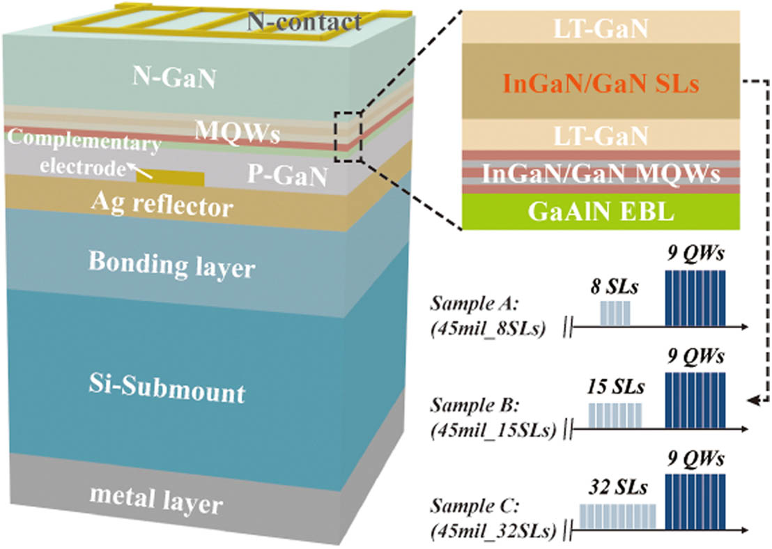
Fig. 1. Schematic of Si-substrate LED vertical structure of the three samples with SL period numbers of 8, 15, and 32.
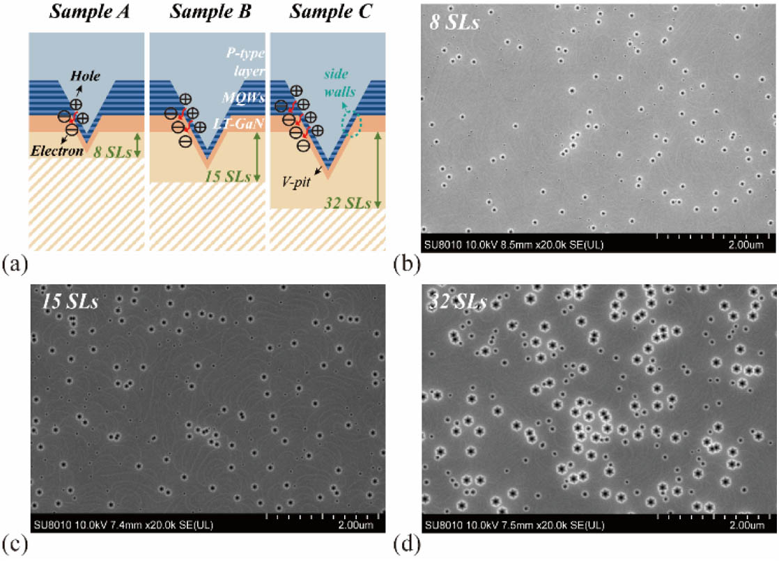
Fig. 2. (a) Schematic of the V-pits and carrier transportation situation for Samples A–C. SEM images of the MQW layer for three LED samples with SL period numbers of (b) 8, (c) 15, and (d) 32.
Fig. 3. Optoelectronic characteristics of LED Samples A, B, and C. (a) Light output power–current–voltage (L-I-V ) characteristics under a CW injection current. (b) EQE under different currents. (c) Luminous efficacy under different currents.
Fig. 4. Electroluminescence (EL) spectra of Samples A, B, and C under various currents.
Fig. 5. Schematic of (a) the bracket and internal circuit structure and (b) layout for the WDM-LED array chip. (c) Graph of the packaged 4 × 4
Fig. 6. (a) CIE diagram of 16 LED pixels under the current of 100 mA. (b) L-I-V characteristics and relative optical power for 16 LED pixels in the WDM-LED array chip.
Fig. 7. (a) Upper: flow block diagram of the digital signal processing (DSP) in our VLC system. Lower: experimental setup of the VLC system. (b) Block diagram of the principle of the MLC algorithm. (AWG, arbitrary waveform generator; OSC, oscilloscope; DMT Mod., DMT modulation; DMT Demod., DMT demodulation; ZF Equ., zero-forcing equalization.)
Fig. 8. VLC performance of LED Samples A, B, and C. (a) − 10
Fig. 9. Schematic of intensity modulation of LEDs with different resistance (R ) and EQE (E ) to explain the data rate gain from LED’s relatively more SL periodicity. (V 0 L c I , current; V , voltage; L , light output power.)
Fig. 10. SNR, allocated bit number, and power ratio versus subcarrier for eight LED channels when BPL-DMT modulation is utilized.
Fig. 11. (a) Data rates versus bandwidth; (b) maximum data rates and BER for eight LED channels. (λ 1 : 456 nm λ 2 : 480 nm λ 3 : 500 nm λ 4 : 526 nm λ 5 : 556 nm λ 6 : 583 nm λ 7 : 631 nm λ 8 : 660 nm
Fig. 12. Data rates versus bandwidths in a 20-m VLC link. Inset: the received QAM signal diagrams at the data rate of 2.02 Gbps.
|
Table 1. Recent Achievements Applying WDM-LEDs

Set citation alerts for the article
Please enter your email address
© Copyright 2018-2021 | Chinese Laser Press. All Rights Reserved 沪ICP备15018463号-20