
Fangchen Hu, Shouqing Chen, Guoqiang Li, Peng Zou, Junwen Zhang, Jian Hu, Jianli Zhang, Zhixue He, Shaohua Yu, Fengyi Jiang, Nan Chi. Si-substrate LEDs with multiple superlattice interlayers for beyond 24 Gbps visible light communication[J]. Photonics Research, 2021, 9(8): 1581
- Photonics Research
- Vol. 9, Issue 8, 1581 (2021)
Abstract
1. INTRODUCTION
Driven by the congestion of available radio frequency spectrum resources and the ever-increasing demand for wireless network capacity in the upcoming sixth-generation (6G) networks [1,2], visible light communication (VLC) using mass-market illumination light-emitting diodes (LEDs) has attracted considerable attention due to the sufficient visible light spectrum resource (400–800 THz) and high data rate (theoretically up to terabytes per second [3]). Additionally, VLC has the potential to be integrated into existing solid-state lighting systems, which enables the combination of illumination and wireless communication [4]. Therefore, many efforts have been made to optimize VLC systems to achieve higher data rates and longer transmission distances for more practical applications [5–9].
Commercially available LEDs usually have a limited modulation bandwidth (MB) of only several megahertz (MHz) [10], which has become one of the biggest challenges for the development of high-speed VLC systems. Various studies have been undertaken to optimize the design of III-nitride LEDs and expand the MB [11,12]. Among them, micro-LEDs are typical candidates of which the MB has been successfully expanded to over hundreds of MHz by manipulatively reducing active areas. Recent studies have shown a record data rate of 5 Gbps with a single micro-LED [13] and over 10 Gbps with an array [14], and the bandwidth has reached 1.06 GHz with a quantum dot micro-LED [15] in a high-speed VLC system. In addition, other reported LEDs, including resonant-cavity LEDs, semi/nonpolar GaN LEDs and GaN nanowire LEDs, also present better bandwidth performance than traditional LEDs [16]. However, most of the reported LEDs are grown on a sapphire substrate with a lateral structure so are always subject to issues of current crowding, poor heat conductivity, and current droop under a high injection current density. In addition, the achieved output optical power of micro-LEDs is only at a magnitude of several milliwatts owing to the small active area, which hardly supports long-distance VLC. Consequently, a different type of novel LED, namely, InGaN/GaN LED fabricated on Si (1 1 1) (Si-substrate LED), has become a promising alternative to overcome the abovementioned problems. Si-substrate LEDs are capable of achieving both high optical output power (almost 100 times that of the micro-LED in Ref. [14]) and high-speed VLC transmission. An aggregate net data rate of 15.17 Gbps has been demonstrated for a 1.2-m underwater VLC link using a Si-substrate LED chip [5]. Si photonics is also deemed as a promising path to realize future optical interconnections and optoelectronic monolithic-integrated circuits [17].
Previous high-speed VLC transmissions based on Si-substrate LEDs are mainly realized by communication algorithm optimization such as advanced modulation formats with novel equalization schemes, rather than a targeted optimization on LED design and fabrication. For example, in these high-speed VLC demonstrations of Refs. [18,19], the utilized Si-substrate LED is just designed for illumination instead of communication, and the data rate improvement attributes to the discrete multitone (DMT) modulation with bit-loading technology or the deep neural network equalizer, which in fact brings limited gain compared to that of the innovation on devices because the upper bound of the communication capacity in a VLC system is essentially determined by the signal-to-noise ratio (SNR) and MB of the utilized optoelectrical devices, particularly of the LED transmitter. To achieve a higher VLC data rate than before, it is important to break through the upper bound by the optimization of the LED structure for communication. Previous Si-substrate LED optimization has always focused on the improvement of luminescence properties, such as internal/external quantum efficiency (IQE/EQE), luminous efficiency, and power consumption [20,21]. Few efforts have been made to improve the communication performance through direct Si-substrate LED design. Therefore, it is meaningful to investigate the impact of different Si-substrate LED parameters on the VLC performance and accordingly design a modified LED transmitter for high-speed VLC systems.
Sign up for Photonics Research TOC. Get the latest issue of Photonics Research delivered right to you!Sign up now
Among Si-substrate LED epitaxial layers, the superlattice interlayer (SL) serves as a significant strain relaxation layer between n-type GaN and InGaN/GaN multiple quantum wells (MQWs) layers to enhance the light emission efficiency and reduce the quantum-confined Stark effect [22]. Since the SL period number has been demonstrated to greatly influence the EQE and forward voltage of Si-substrate LEDs [23], its distinct impact on optoelectrical characteristics may also affect the communication performance during the signal modulation process. As a result, we for the first time studied the effect of SL period number on the VLC performance by systematically measuring and analyzing the optoelectrical characteristics and VLC performance of three LED samples with different SL period numbers. The measured optoelectrical characteristics consist of light output power–current–voltage (L-I-V) relation, EQE, luminous efficacy, and spectrum of the LED sample. The measured VLC performance includes bandwidth, SNR, and maximum achievable data rate of the VLC system with the LED sample. It is found that relatively more SLs could enhance both the luminescence and communication properties of Si-substrate LEDs via the decrease of resistance, improvement of EQE, and extension of bandwidth. A preliminary interpretation for the positive effect on communication is also given for discussion that the decrease of resistance and improvement of EQE could improve the modulation efficiency of LED by amplifying the amplitude of the output optical signal.
Next, we designed and fabricated a single integrated ultrahigh-capacity wavelength-division-multiplexing (WDM)-LED array chip with 16 different wavelengths as future potential VLC channels. Unlike our previous work of Ref. [5] that the utilized five-color Si-substrate LED is originally designed for white-light illumination without any modification in the LED inner-structure for VLC, in this work, every LED pixel in our LED array chip is specially optimized with the optimal SL period number of 32 which helps the data rate exceed the previous one. With eight of these different wavelengths, up to 24.25 Gbps ultrahigh data rate is experimentally demonstrated by a modified bit and power loading (MBPL)-DMT modulation. As far as we are aware of, this is the highest VLC capacity achieved by an InGaN/GaN LED. To highlight the long-distance VLC ability of Si-substrate LEDs, we also demonstrated a long-distance high-speed VLC link using a single Si-substrate blue LED pixel with a record-breaking data rate of 2.02 Gbps as far as a 20-m distance. To the best of our knowledge, this is the highest data rate for 20-m free-space LED-based VLC. These two applications demonstrate the flexibility and superiority of the Si-substrate LED for both high-speed and long-distance VLC communication while validating the effectiveness of optimizing the SL period number for VLC-use Si-substrate LED design.
2. FABRICATION AND CHARACTERIZATION
A. Si-Substrate InGaN/GaN LED with Multiple Superlattice Layers
We prepared three Si-substrate LED samples with SL period numbers of 8, 15, and 32, respectively, for comparison experiments. The edge length of all samples is 45 mil. The LED samples are grown on a patterned silicon (111) substrate fabricated by close-coupled showerhead metal-organic chemical vapor deposition from the Thomas Swan company. According to the standard epitaxial growth process of Si-substrate LEDs in Ref. [24], the epitaxial structure starts with a 110-nm high-temperature AlN (HT-AlN) buffer layer, followed by a Si-doped N-type GaN layer and a 10-nm low-temperature GaN (LT-GaN) layer. Subsequently, an SL with a certain period number was deposited, followed by a 10-nm LT-GaN layer, nine periods of InGaN/GaN MQWs (the refractive index is 2.45), a 10-nm p- electron blocking layer, and 100-nm Mg-doped P-GaN. The SL period number could be accurately manipulated during the epitaxial growth.
Once epitaxial growth is finished, the standard vertical Si-substrate LED fabrication process is followed. The schematic of the Si-substrate LED vertical structure is depicted in Fig. 1. First, the epitaxial wafer is cleared and processed with the P-type annealing in the superalloy furnace. The annealing temperature is controlled and adjusted by the temperature of the metal layer alloy. To increase single-side luminescence, we use an electron beam evaporator to deposit a layer of Ag on the clean epitaxial wafer. The Ag has good ohmic contact with the P-GaN. Additionally, a high resistance complementary electrode is deposited between the Ag reflection layer and P-GaN to alleviate current crowding and increase single-side luminescence. Then, the film is transferred to the top of a new Si-submount (P-type doping, resistance ) with a width of 200 μm. The Si-submount has good conductive and thermal conductivity and is bounded with the film by the Au–Au bonding or Au–Sn bonding method. One side of the Si-submount is a bonding layer. Another side of the Si-submount is a vapor-deposited CrAu metal layer. Next, the original Si-substrate connected to the N-GaN layer is etched by the mixed solution of HF, , and . The exposed N-GaN is immersed in 85°C and 20% mass concentration KOH solution for surface coarsening to improve light extraction efficiency. Finally, the N-contact is processed on the pre-roughened N-GaN, and the vertical structure LED film is completed with the advantages of single-side light emission, better luminescent uniformity, and better luminescent unidirectivity. The optical reflectance is monitored by an ultraviolet spectrophotometer.
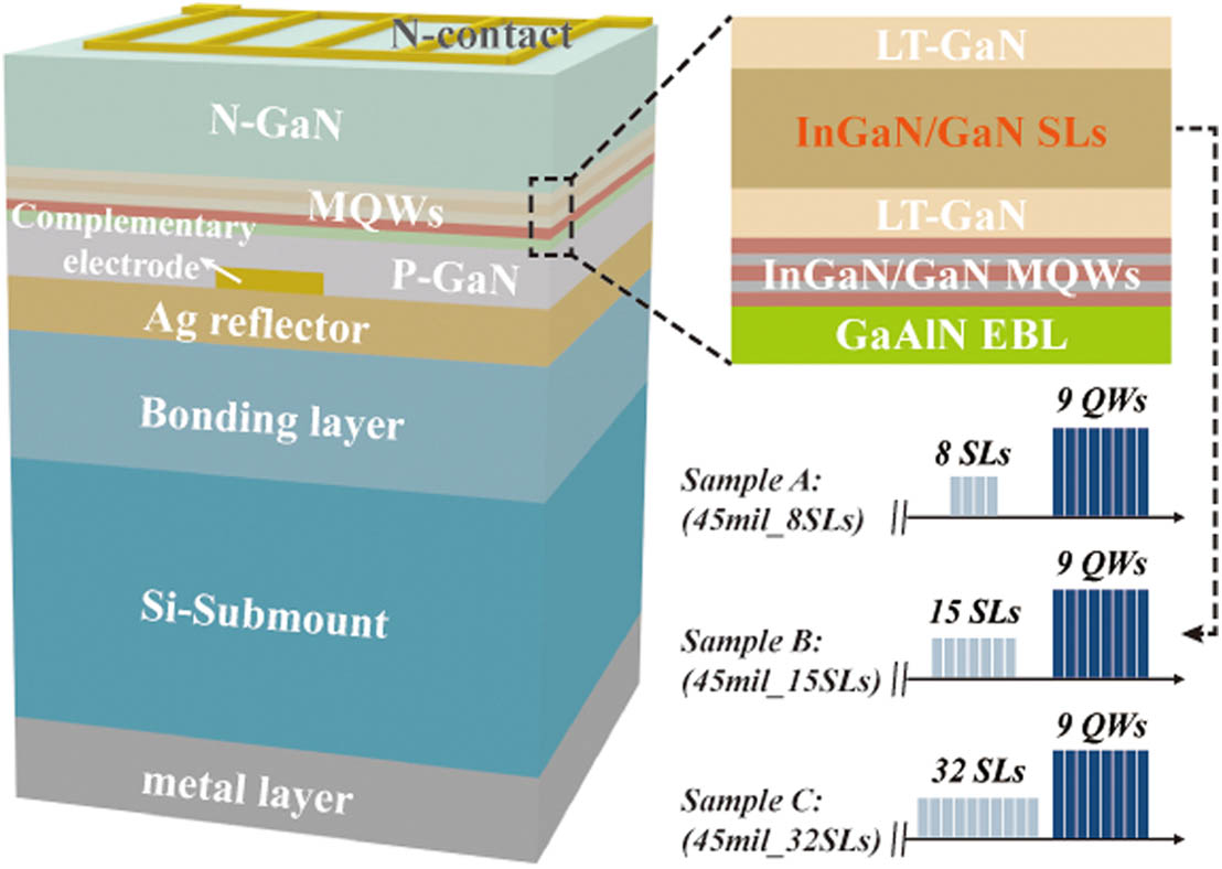
Figure 1.Schematic of Si-substrate LED vertical structure of the three samples with SL period numbers of 8, 15, and 32.
The last step is to complete the LED chip packaging and light concentration. The LED is directly attached to the heat sink of the LED bracket using a highly-heat-conductive and high-adhesion paste (CT285). Subsequently, the golden wires are utilized to realize the electrical connection between the LED chip and bracket by a golden wire ball ultrasonic welding machine. The diameter of the golden wire is 20 μm. To confine the output light from the LED, a lens with the standard Lumileds packaging is assembled on the top of the LED chip. It could suppress the emission angle within 120°. The gap between the lens and bracket is filled up with the high-transmittance and high-refraction epoxy silicone (Dow Corning OE-6662, refractive index 1.53, transmittance 90%). Finally, the LED chip is heated in an oven at 150°C and the silicone is kept curing for one hour.
The scanning electron microscopy (SEM) images of the MQWs layer for the three LED samples are shown in Figs. 2(b)–2(d), which helps us intuitively observe the LED morphology difference when the SL period number is changed. Inverted V-shaped hexagonal pits (V-pits) are randomly distributed on the surface of the MQWs layers. With an increase in the SL period number, the size of the V-pits is gradually enlarged. Figure 2(a) is used to explain why the size of V-pits will enlarge with the increase of SL period number and theoretically analyze the potential effect on LED characteristics induced by the growth of V-pits. The SL beneath the LT-GaN provides space for the formation of V-pits embedded within the MQWs. Since the intersection angle of the V-pit is fixed at 56°, determined by the (10_11)-oriented sidewall, an increase in the SL period number must lead to an increase in the size of the V-pits. The sidewall of the V-pits has a lower effective height for hole injection than for the flat region of the MQWs; therefore, the larger the pit size, the easier the hole is injected into the MQWs, i.e., the lower the overall resistance of LED samples with more SLs. In addition, larger V-pits enhance threading dislocation screening, which will improve the light extraction efficiency and mitigate the droop effect. The carrier lifetime also decreases due to the improved carrier recombination through a larger-area sidewall of V-pits.
![]()
Figure 2.(a) Schematic of the V-pits and carrier transportation situation for Samples A–C. SEM images of the MQW layer for three LED samples with SL period numbers of (b) 8, (c) 15, and (d) 32.
The optoelectronic characteristics of three LED samples, including L-I-V relation, EQE, luminous efficacy, and spectrum of the LED sample, were measured by a Keithley Instruments 2635A source meter and an Instrument Systems CAS 140CT spectrometer. Figure 3(a) shows the L-I-V characteristics under a continuous wave (CW) injection current. The I-V curve shows that Sample C with the most SL period number has the lowest forward voltage and Sample A with the least SL period number has the highest forward voltage. An LED with a low forward voltage means it has a low overall resistance according to the Ohm’s law. Hence, the increase of SL period number could reduce the overall resistance, which is consistent with the analysis on V-pits before. The I-L curve indicates that the increase of SL period number from Sample A to Sample C greatly improves the LED’s output optical power. At the current of 750 mA, the output power of Samples B and C even reaches the watt level, which means the Si-substrate LED with 15 or 32 SLs could support a long-distance VLC link. In addition, the measured I-L curve of Sample C shows a better linearity than that of Sample A from 0 to 750 mA, which creates an opportunity for ultrahigh-speed modulation using Sample C. The nonlinear effect would be minor if a high-amplitude signal is modulated to Sample C. In optical communication, it is well known that nonlinear effect dramatically limits the amplitude of transmitted signal, but a high signal amplitude is necessary for a high data rate requiring high SNR. From this perspective, the Si-substrate LED with 32 SLs that has a great modulation linearity is more suitable for high-speed VLC. Figure 3(b) is the EQE of three LED samples when injected with different currents. The EQEs of Samples B and C reach a maximum of 68% near the injection current of 50 mA. The LED with a higher EQE can emit more light instead of the undesired heat when given a certain amount of electrical power. With the continuous increase of the injection current, Samples B and C begin to suffer from the droop effect, but their EQEs remain above 52% below the current of 750 mA. The EQE of Sample A is the lowest only around 35%. The EQE difference between the three samples reveals that an increase in the SL period number provides a significant EQE gain from eight SL periods to 15 SL periods through the strain relief of the MQWs, while a period number greater than 15 is close to the EQE gain limit, with little gain obtained by further increasing the SL period number to 32. The luminous efficacy of the three samples [Fig. 3(c)] ranges from 25 to 35 lm/W, which has satisfied the regular illumination requirement. Within the current of 100 mA, the luminous efficacy of Sample C is higher than that of Sample B, which is higher than that of Sample A. Figures 4(a)–4(c) present the optical spectrum and electroluminescence (EL) intensity of Samples A–C. The results show that the difference in SL period number does not shift the peak wavelength horizontally, but more SLs improve the EL intensity.
![]()
Figure 3.Optoelectronic characteristics of LED Samples A, B, and C. (a) Light output power–current–voltage (
![]()
Figure 4.Electroluminescence (EL) spectra of Samples A, B, and C under various currents.
From the criteria of efficient solid-state lighting [25], an efficient LED tends to have a low forward voltage, high EQE, and luminous efficacy to achieve the highest output optical power using the lowest amount of electrical power. Therefore, the Si-substrate LED with 32 SLs (Sample C) is the most efficient LED sample for illumination compared to the other samples according to the measured optoelectrical characteristics. Additionally, the great linearity of the I-L curve and high output optical power of Sample C are beneficial for high-speed and long-distance VLC transmission. That is to say, relatively larger SL period numbers could enhance the luminescence properties and the nonlinear effect resistance of the Si-substrate LED. Interestingly, besides the nonlinear effect resistance, relatively more SL periods also significantly improve the communication properties by increasing the SNR, which will be specifically analyzed and explained in Section 4.
Considering the positive effect of 32 SLs for both luminescence and communication properties of Si-substrate LEDs, we designed and fabricated an integrated Si-substrate WDM-LED array chip, in which the SL period number of every LED pixel is fixed to 32. A higher VLC data rate than before is expected using this modified LED chip with WDM technology and advanced modulation technologies. Since GaN is more efficient in short wavelength material, the body material of blue, green, and yellow LED pixels is GaN, but that of red LED pixel is AlGaInP, which is more efficient for long-wavelength material. The specific epitaxial growth and fabrication process of blue, green, yellow, and red LED pixels in the WDM-LED array chip can be studied in Refs. [20,21,24,26].
Figure 5(a) shows the internal circuit design and bracket structure of the proposed WDM-LED array chip. There is a heat sink array in the middle. Every part of the array serves as a P-pad [also seen in Fig. 5(d)] for every LED pixel and connects together as a common anode which is then connected to four ground pins in the corner. This special common anode design aims to reduce the low-frequency response of a VLC system, and thereby alleviates the saturation effect in low-frequency components. Next to every P-pad, there are 16 smaller Au contacts connected to 16 individual cathode pins and their adjacent LED pixels, known as N-pads shown in Fig. 5(d). Using golden wires as a bridge, these N-pads inject signal from the cathode pins into the LED pixels. Figure 5(b) is the schematic of the WDM-LED array chip layout. There are 16 vertical-structure Si-substrate LED pixels with 16 different visible-light wavelengths, including 456, 460, 467, 480, 491, 500, 509, 518, 526, 534, 543, 556, 569, 583, 631, and 660 nm, packaged into one single LED lamp. The lens uses the Lumileds packaging. Light is emitted from the top of the LED pixels. Figures 5(c) and 5(d) are the magnified micrographs of the packaged WDM-LED array chip and every LED pixel. Due to the slight fabrication difference for different color LEDs, the sizes of the blue and green LEDs are 27 mil, yellow LEDs are 45 mil, and red LEDs are 42 mil.
![]()
Figure 5.Schematic of (a) the bracket and internal circuit structure and (b) layout for the WDM-LED array chip. (c) Graph of the packaged
Figure 6(a) shows the Commission Internationale de l’Eclairage (CIE) diagrams for 16 LED pixels under the current of 100 mA. The accurate chromaticity coordinates could be read from this figure. The L-I-V characteristics and relative optical power of the WDM-LED array chip are also measured. The results of eight wavelengths are shown in Fig. 6(b). These wavelengths are also the selected channels for subsequent VLC tests considering their relatively wide wavelength interval (wider than 20 nm). Too narrow wavelength interval will introduce serious cross talk for each channel. Results reveal blue and green LEDs have a higher forward voltage and higher optical power than red and yellow LEDs under the same current. Yellow LEDs have the lowest optical power which is restricted by limited quantum efficiency. There is good linearity for the L-I curves of all colors in our designed Si-substrate LED chips.
![]()
Figure 6.(a) CIE diagram of 16 LED pixels under the current of 100 mA. (b)
3. PRINCIPLE AND EXPERIMENTAL SETUP
To evaluate the VLC performance when using LED Samples A–C and the Si-substrate WDM-LED array chip as VLC transmitters, we tested their maximum achievable data rate based on the BPL-DMT modulation and the experimental setup in Fig. 7. Notedly, a 20-m high-speed VLC experiment also uses a similar experimental setup in Fig. 7. Only the transmitter and transmission distance are changed to a single blue Si-substrate LED and 20-m link, respectively. It is well known that the floor bit-loading (FBL) technology has been widely used in high-speed VLC systems [5,27] to obtain a high spectral efficiency (SE). The optimal bit number allocated to each subcarrier of the DMT signal is set to the integer, of which the value is rounded down from the ideal transmitted entropy referred to the relationship among SNR, bit error ratio (BER), and bit number [28]. Therefore, such a bit assignment is imperfect, and there exists an inevitable SNR gap between the estimated SNR at the th subcarrier (SNR) and the required SNR [] at a target BER for the current allocated bit number at the th subcarrier (). This SNR gap is known as the current margin (CM) [29], which indicates part of the preset power is wasted if the power ratio at every subcarrier keeps identical. Hence, the allocated power ratio at every subcarrier should also be optimized along with bit optimization. The Levin–Campello (LC) algorithm is such a good bit and power joint optimization method for the bit rate maximization problem under a fixed amount of energy [30,31]. In addition, the channel of VLC is uneven, suffering from severe frequency fading issue, which causes the peak bit number to only assemble on several subcarriers, sometimes only two to three subcarriers. Despite the high bit number being desired for a higher data rate, there is a high bit error possibility at these peaks of which the adjacent subcarriers have different bit numbers. A uniform and step-shaped bit distribution is optimal for a better BER performance according to the experience. In addition, more power budget is needed for the high-order quadrature-amplitude-modulation (QAM) signal to increase 1 order compared to the low-order QAM signal. For example, there is a 2.96 dB gap between and , but only 2.83 dB for the power difference between and . Therefore, if the subcarriers with the peak bit number are sparsely distributed and the amount is small, they can be manually subtracted one bit, and the extra power is transferred to other subcarriers. A better BER performance of the modified LC (MLC) algorithm has been demonstrated by experiments.
![]()
Figure 7.(a) Upper: flow block diagram of the digital signal processing (DSP) in our VLC system. Lower: experimental setup of the VLC system. (b) Block diagram of the principle of the MLC algorithm. (AWG, arbitrary waveform generator; OSC, oscilloscope; DMT Mod., DMT modulation; DMT Demod., DMT demodulation; ZF Equ., zero-forcing equalization.)
The flow block diagram of MBPL-DMT modulation is shown in the upper part of Fig. 7(a). At the transmitter side, the transmitted binary signal sequences at every subcarrier are first mapped to different QAM signal sequences with the aid of MBPL technology, which consists of two key steps: SNR estimation and MLC algorithm. For SNR estimation, a quadratic phase-shift keying (QPSK) signal sequence with identical power distribution at each subcarrier serves as the training sequence to estimate the SNR at every subcarrier. According to Ref. [28], the SNR at the th subcarrier (, in dB) can be estimated based on the error vector magnitude at the th subcarrier () of the training sequence, which is given by
Here is always set to 1 for every step of CM assignment. Once the allocation satisfies efficient [31], the optimal power and bit allocation are finished. For instance, in Fig. 7(b), the power margin is assigned to the first and second subcarriers which have lowest compared to other subcarriers. The third subcarrier will not receive any extra power because the current allocation has satisfied efficient. The ultimately averaged SE () is given as
After the modified bit and power loading, standard DMT modulation [33] and normalization are followed to generate the transmitted MBPL-DMT signal which is then fed into an arbitrary waveform generator (AWG). In the schematic of our VLC experimental setup [Fig. 7(a)], the analog signal generated from the AWG is initially pre-equalized by a hardware equalization circuit to extend the bandwidth [34]. Next, the signal is amplified by an electrical amplifier (Mini-Circuits ZHL-6A-S+) and coupled with direct current using a bias tee (Mini-Circuits ZFBT-4R2GW-FT+). For the WDM-LED array chip, 16 channels of the transmitted signal can be independently modulated into every LED pixel. Two plano–convex lenses at the transmitter side and a plano–convex lens at the receiver side were used to guide the incoming light onto an adjustable neutral density (ND) filter (Daheng Optics, GCO-0702M) followed by optical filters and PIN photodetectors (Hamamatsu S10784). The ND filter is coated with a broadband NiCrFe light reduction film allowed for the spectrum from 400 to 700 nm. All wavelengths of eight channels are included in the working spectrum of the ND filter. The used optical filter is a two-cavity optical filter proposed in Ref. [35], and it includes multilayer films deposited alternatively by Ta2O5 and SiO2. The peak wavelength and bandwidth of the optical filter can be continuously tuned by adjusting the thickness of every film. Here, the transmission wavelength of the passband of each optical filter is just the peak wavelength of eight channels and the bandwidth of the passband is 20 nm, which is the minimum wavelength interval between two channels. The narrow bandwidth could guarantee minimum cross talk between two channels. Moreover, the transmission of the ND filter has been proved to be higher than 90% to minimize the power of the peak wavelength. Despite that part of the optical power in every channel is inevitably lost, the power loss will not distinctly decrease the data rate because the Si-substrate LED originally has a watt-level output optical power. The power loss can be mitigated by increasing the bias current to increase the emitted optical power. Every PIN was connected to a trans-impedance amplifier (Maxim Integrated, MAX3665) and two electrical amplifiers (Mini-Circuits ZHL-6A-S+). Finally, 16 paths are sent to an oscilloscope (Agilent, MSO9254A) for further signal processing. The differential receiver configuration is beneficial to common-mode noise reduction.
At the receiver’s digital signal processing part, the received signal is resampled and demodulated to the QAM signal according to the standard DMT demodulation process followed by a one-tap zero-forcing (ZF) equalization. To enhance the effectiveness of phase recovery and SNR estimation, intra-symbol frequency-domain averaging (ISFA) is applied to flatten the response. In addition, the sampling frequency offset (SFO) always happens due to the clock asynchronization of the digital-to-analog converter in the transmitter and analog-to-digital converter. It will lead to amplitude reduction, phase rotation, and intercarrier interference, which will dramatically deteriorate the SNR [36]. To alleviate the SFO, two DMT symbols at the head and tail of the entire DMT signal sequence serve as the pilots to estimate SFO. Applying the linear polynomial fitting method, the SFO at the rest of the DMT symbols is accurately estimated. After the ZF equalization, ISFA, and phase recovery, the SNR at every subcarrier can be accurately estimated through the received and transmitted QPSK training sequence. Finally, the recovered QAM signal is demapped to decimal symbols and binary bits for BER calculation.
4. VLC RESULTS AND DISCUSSION
Based on the setup in Fig. 7, the communication performances of Samples A–C with different SL period numbers are measured over a 1.2-m VLC link, including the -10-dB bandwidth, SNR, and achievable data rate. Results are shown in Fig. 8. Sample A has the lowest bandwidth in the current range of 0–250 mA, while Samples B and C have similar bandwidth levels, but their bandwidths are both higher than that of Sample A because a higher SL period number helps reduce the carrier lifetime. When the injection current increases, the bandwidth of all samples converges to the same value because the resistor–capacitor (RC) time constant now is the dominant limitation on the bandwidth instead of carrier lifetime. The RC constants of the three samples are similar due to their identical LED sizes of 45 mil. Figure 8(b) is the SNR curves of three LED samples when they are injected with their optimal injection current and peak-to-peak voltage which could achieve the highest SNR. The average SNR increases as the SL period number increases. An approximately 4-dB gain from Sample A to Sample B and an approximately 2-dB gain from Sample B to Sample C are found at the frequency point of 200 MHz. Subsequently, the maximum data rates of three samples are measured using MBPL-DMT modulation. By iteratively changing the bandwidth of the signal, the maximum data rates of Samples A, B, and C are 2.48 Gbps, 2.97 Gbps, and 3.37 Gbps, respectively [Fig. 8(c)]. All BERs of the data reach the 7% forward error code threshold, so the data rate is real and represents the maximum achievable data rate of the measured LED. The 3.37-Gbps data rate is the highest data rate for single blue Si-substrate LED-based VLC systems, which greatly benefits from the optimization of the SL period number.
![]()
Figure 8.VLC performance of LED Samples A, B, and C. (a)
As a result, the LED sample with 32 SLs not only has the best luminescence properties, such as high EQE and low forward voltage, but also has the highest SNR and data rate. This finding reveals that some optimization on LED parameters also brings the improvement of communication performance, such as the SLs period number in this paper. Here we give a preliminary explanation of why the increase of SL period number would offer a remarkable gain of data rate by the schematic of modulation process of LED illustrated in Fig. 9. First, the -dB bandwidth of the LED is extended by more SL period numbers due to the improved LED crystal quality. Second, the increase of SLs reduces the overall resistance which amplifies the amplitude of the current signal. In Fig. 9, the slope of the V-I curve indicates the resistance of an LED. The lower the slope, the lower the resistance. The with the lowest resistance produces the highest amplitude of the responding current signal . Third, the increase of SLs significantly improves the EQE, which causes the increase of the amplitude of the optical signal. In Fig. 9, the slope of the L-I curve represents the EQE. A higher EQE helps the LED output an optical signal with a higher amplitude. This can also be explained by the deviation of LED output power based on the classical carrier recombination rate equalization below [37]:
![]()
Figure 9.Schematic of intensity modulation of LEDs with different resistance (
Overall, the reduction of carrier lifetime, overall resistance, and the improvement of the EQE from the relative increase of the SL period number synergistically improve the SNR by enhancing the modulation efficiency of a Si-substrate LED. A good Si-substrate LED for high-speed VLC should have the characteristics of short carrier lifetime, low resistance, and high EQE. Relatively increasing SL period number is one of the optimization methods. However, it is noted that the SL period number cannot be increased infinitely because excess serial resistance induced by the rise of LED thickness will inverse the overall resistance variation trend with SL periodicity. When the SL period number increases to a maximum value so that the LED’s thickness becomes the dominant factor of overall resistance instead of the hole injection enhancement, the modulation efficiency of an LED will be optimal and starts to fall if the SL period number keeps increasing according to our analysis. Therefore, the selection of an optimal SL period number, or more broadly, of an optimal Si-substrate LED for VLC, could be obtained by monitoring the overall resistance and EQE of the LED. Apparently, a lot of LED samples with different SL period numbers are required to find the best parameter. Here, this paper only provides the analysis of the effect of the SL, unable to find the best period number limited by the number of different LED samples.
Next, the VLC results of Si-substrate WDM-LED array chips are analyzed below. Initially, the recent VLC achievements using WDM LEDs are summarized in Table 1. Most of the high-speed VLC systems are realized by Si-substrate LEDs or uLEDs. The highest transmission speed of 20.08 Gbps is achieved by a similar WDM-LED array chip, but the channel is an underwater channel, and the modulation format is probabilistic-shaped bit-loading DMT modulation. The source entropy allocated by probabilistic shaping technology is set to the value of Shannon limit in this demonstration, which is not the optimal way. The optimally allocated entropy should be higher than the Shannon limit to take advantage of the forward error code. This suitable entropy is hardly determined and needs massive calculation simulation based on Gaussian channel [44]. On the other hand, the MBPL algorithm is more convenient in the optimal entropy determination than probabilistic-shaped (PS) bit-loading technology, because the MLC algorithm is mature and automatical for SE allocation. In addition, the gain of data rate from MBPL is also at a similar level as PS technology. Hence, we tested the Si-substrate WDM-LED array chip based on the MBPL-DMT modulation. Figure 10 shows the SNR, bit allocation, and power ratio for every utilized LED channel after MBPL technology at their highest data rate case. To alleviate the pressure on the optical filter on the receiver side, only eight LED channels (456, 480, 500, 526, 556, 583, 631, and 660 nm) have a minimum wavelength interval of more than 20 nm. Though the bit number in some subcarriers could reach 8 bit/Hz after estimation, the number of these peak subcarriers is few. Therefore, these peak subcarriers are pruned according to the MLC algorithm; thus it is observed that the maximum bit number is 7 bit/Hz in Fig. 10. Power ratios also flustrate along with the SNR and allocated bit, ranging from 0.4 to 1.6. Figure 11(a) shows the relation between the final data rate and the signal bandwidth for eight channels. As the sample rate of the AWG increases, the signal bandwidth varies from 475 to 600 MHz, the data rates of eight channels rise at first thanks to the modulation bandwidth expansion, and then decline due to the bandwidth limitation of the LED itself. From the wavelength of 456–660 nm, the maximal data rates [Fig. 10(b)] are 3.32 Gbps, 3.19 Gbps, 3.26 Gbps, 2.80 Gbps, 2.54 Gbps, 2.27 Gbps, 3.41 Gbps, and 3.46 Gbps, respectively. The aggregated data rate is 24.25 Gbps under the 7% forward error correction (FEC) threshold (3.8 × 10⁻³). Since green/yellow LEDs have a worse crystal quality than blue/red LEDs, thus the maximum data rate of the green/yellow LEDs is also lower than that of the blue/red LEDs. This application validates the ultrahigh communication capacity potential of beyond 20 Gbps using Si-substrate LEDs and WDM technology. If optical filter technology could support the division of more than eight wavelengths in the future, then more visible light channels can be utilized, and a higher communication data rate will be possible using Si-substrate LEDs. Recent Achievements Applying WDM-LEDsLED Type Modulation Format Data Rate (Gbps) Distance Data Source Si-LED (8 colors) PS-bit-loading-DMT 20.08 1.2 m underwater OFC 2020 [ uLED (RGBY) Bit-loading OFDM 15.73 1.6 m free space JLT 2019 [ Si-LED (RGBYC) Bit-loading DMT 15.17 1.2 m underwater PR 2019 [ Si-LED (RGBYC) DFTS-OFDM 14.6 1.2 m underwater OFC 2019 [ Si-LED (RGBYC) DMT 10.72 1.2 m underwater OFC 2018 [ uLED (RGBY) Bit-loading OFDM 10.2 Free space ECOC 2018 [ uLED (RGBY) + RC-LED (R) Bit-loading OFDM 10.04 1.5 m free space JLT 2016 [ LED (RGB) CAP 8 1 m free space PJ 2015 [
![]()
Figure 10.SNR, allocated bit number, and power ratio versus subcarrier for eight LED channels when BPL-DMT modulation is utilized.
![]()
Figure 11.(a) Data rates versus bandwidth; (b) maximum data rates and BER for eight LED channels. (
To highlight the advantage of watt-level optical output power when using Si-substrate LEDs, a 20-m/2.02-Gbps free-space VLC demonstration is carried out using Sample C. At the receiver side, a Fresnel lens is added, which is used to enlarge the receiver area and increase the SNR. Figure 12 shows the data rate under different bandwidths. At the signal bandwidth of 375 MHz, a recorded data rate of 2.02 Gbps over a 20-m distance is successfully realized using a single blue Si-substrate pixel with 32 SLs (Sample C). The diagrams of the allocated QAM signal are plotted in the insets of Fig. 12. Notably, only a 1.71-Gbps/20-m rate has previously been achieved for micro-LEDs, even using an LED array with nine pixels [14].
![]()
Figure 12.Data rates versus bandwidths in a 20-m VLC link. Inset: the received QAM signal diagrams at the data rate of 2.02 Gbps.
5. CONCLUSION
In this paper, we for the first time investigated the impact of different SL period numbers on the Si-substrate LED-based VLC performance. Through a comparison experiment using LEDs with SL period numbers of 8, 15, and 32, we found that a moderate increase of SL period number could not only achieve efficient luminescence by reducing forward voltage and increasing EQE, but also increase the achievable VLC data rate by extending the bandwidth and enhancing the modulation efficiency of the LED. It is preliminarily explained that the enhancement on modulation efficiency results from the amplification of the amplitude of output optical signal by resistance reduction and EQE improvement. Hence, the optimal optoelectrical characteristics of the Si-substrate LED for high-speed VLC can consist of three points: short carrier life, low overall resistance (i.e., low overall resistance), and high EQE. Increasing the SL period number is one of the practical methods to realize these optimal optoelectrical characteristics. However, it is noted that the SL period number cannot be increased infinitely because resistance of the LED will rise again if the SL is too thick. There must exist an optimal SL period number to achieve the highest VLC data rate, which can be found by parameter iteration work in the future. Based on the currently optimal SL period number of 32, we for the first time fabricated a single integrated ultrahigh capacity WDM-LED array chip with 16 different wavelengths as future potential VLC channels. The Si-substrate LED with vertical structure has the advantages of super-linear I-L response, high optical output power, and EQE, and thus is suitable for both high-speed and long-distance VLC transmission. Hence, two proof-of-concept experiments with record-breaking transmission speed for both short- and long-distance VLC links are successfully achieved by BPL-DMT modulation. First, we achieved a data rate of 24.25 Gbps over a 1.2-m VLC link using the Si-substrate WDM-LED array chip. Second, we realized a data rate of 2.02 Gbps over a 20-m VLC link by a blue Si-substrate LED with 32 SL period number. To the best of our knowledge, 24.25 Gbps is the highest capacity for an InGaN/GaN LED-based VLC system, and 2.02 Gbps is the highest data rate for 20-m free-space LED-based VLC. More LED parameters should be investigated especially for VLC to pave the way for ultrahigh-capacity VLC in the future.
References
[1] N. Chi, Y. Zhou, Y. Wei, F. Hu. Visible light communication in 6G: advances, challenges, and prospects. IEEE Veh. Technol. Mag., 15, 93-102(2020).
[2] E. C. Strinati, S. Barbarossa, J. L. Gonzalez-Jimenez, D. Ktenas, N. Cassiau, L. Maret, C. Dehos. 6G: the next frontier: from holographic messaging to artificial intelligence using subterahertz and visible light communication. IEEE Veh. Technol. Mag., 14, 42-50(2019).
[3] L. E. M. Matheus, A. B. Vieira, L. F. M. Vieira, M. A. M. Vieira, O. Gnawali. Visible light communication: concepts, applications and challenges. IEEE Commun. Surveys Tuts., 21, 3204-3237(2019).
[4] G. Corbellini, K. Aksit, S. Schmid, S. Mangold, T. R. Gross. Connecting networks of toys and smartphones with visible light communication. IEEE Commun. Mag., 52, 72-78(2014).
[5] Y. Zhou, X. Zhu, F. Hu, J. Shi, F. Wang, P. Zou, J. Liu, F. Jiang, N. Chi. Common-anode LED on a Si substrate for beyond 15 Gbit/s underwater visible light communication. Photon. Res., 7, 1019-1029(2019).
[6] N. Chi, Y. Zhou, S. Liang, F. Wang, J. Li, Y. Wang. Enabling technologies for high-speed visible light communication employing CAP modulation. J. Lightwave Technol., 36, 510-518(2018).
[7] M. S. Islim, R. X. Ferreira, X. He, E. Xie, S. Videv, S. Viola, S. Watson, N. Bamiedakis, R. V. Penty, I. H. White, A. E. Kelly, E. Gu, H. Haas, M. D. Dawson. Towards 10 Gb/s orthogonal frequency division multiplexing-based visible light communication using a GaN violet micro-LED. Photon. Res., 5, A35-A43(2017).
[8] Y. Wang, X. Huang, J. Shi, Y.-Q. Wang, N. Chi. Long-range high-speed visible light communication system over 100-m outdoor transmission utilizing receiver diversity technology. Opt. Eng., 55, 056104(2016).
[9] F. Hu, J. A. Holguin-Lerma, Y. Mao, P. Zou, C. Shen, T. K. Ng, B. S. Ooi, N. Chi. Demonstration of a low-complexity memory-polynomial-aided neural network equalizer for CAP visible-light communication with superluminescent diode. Opto-Electron. Adv., 3, 200009(2020).
[10] X. Huang, Z. Wang, J. Shi, Y. Wang, N. Chi. 1.6 Gbit/s phosphorescent white LED based VLC transmission using a cascaded pre-equalization circuit and a differential outputs PIN receiver. Opt. Express, 23, 22034-22042(2015).
[11] E. Xie, X. He, M. S. Islim, A. A. Purwita, J. J. D. McKendry, E. Gu, H. Haas, M. D. Dawson. High-speed visible light communication based on a III-nitride series-biased micro-LED array. J. Lightwave Technol., 37, 1180-1186(2019).
[12] X. Xiao, H. Tang, T. Zhang, W. Chen, W. Chen, D. Wu, R. Wang, K. Wang. Improving the modulation bandwidth of LED by CdSe/ZnS quantum dots for visible light communication. Opt. Express, 24, 21577-21586(2016).
[13] R. X. G. Ferreira, E. Xie, J. J. D. McKendry, S. Rajbhandari, H. Chun, G. Faulkner, S. Watson, A. E. Kelly, E. Gu, R. V. Penty, I. H. White, D. C. O’Brien, M. D. Dawson. High bandwidth GaN-based micro-LEDs for multi-Gb/s visible light communications. IEEE Photonics Technol. Lett., 28, 2023-2026(2016).
[14] E. Xie, R. Bian, X. He, M. S. Islim, C. Chen, J. J. D. McKendry, E. Gu, H. Haas, M. D. Dawson. Over 10 Gbps VLC for long-distance applications using a GaN-based series-biased micro-LED array. IEEE Photonics Technol. Lett., 32, 499-502(2020).
[15] Z. Wei, L. Zhang, L. Wang, C.-J. Chen, A. Pepe, X. Liu, K.-C. Chen, Y. Dong, M.-C. Wu, L. Wang. High-speed visible light communication system based on a packaged single layer quantum dot blue micro-LED with 4-Gbps QAM-OFDM. Optical Fiber Communications Conference and Exhibition (OFC), 1-3(2020).
[16] S. Rajbhandari, J. J. D. McKendry, J. Herrnsdorf, H. Chun, G. Faulkner, H. Haas, I. M. Watson, D. O’Brien, M. D. Dawson. A review of gallium nitride LEDs for multigigabit-per-second visible light data communications. Semicond. Sci. Technol., 32, 023001(2017).
[17] Y. Sun, K. Zhou, Q. Sun, J. Liu, M. Feng, Z. Li, Y. Zhou, L. Zhang, D. Li, S. Zhang, M. Ikeda, S. Liu, H. Yang. Room-temperature continuous-wave electrically injected InGaN-based laser directly grown on Si. Nat. Photonics, 10, 595-599(2016).
[18] Y. Zhou, Y. Wei, F. Hu, J. Hu, Y. Zhao, J. Zhang, F. Jiang, N. Chi. Comparison of nonlinear equalizers for high-speed visible light communication utilizing silicon substrate phosphorescent white LED. Opt. Express, 28, 2302-2316(2020).
[19] N. Chi, Y. Zhao, M. Shi, P. Zou, X. Lu. Gaussian kernel-aided deep neural network equalizer utilized in underwater PAM8 visible light communication system. Opt. Express, 26, 26700-26712(2018).
[20] Q. Lv, J. Liu, C. Mo, J. Zhang, X. Wu, Q. Wu, F. Jiang. Realization of highly efficient InGaN green LEDs with sandwich-like multiple quantum well structure: role of enhanced interwell carrier transport. ACS Photonics, 6, 130-138(2019).
[21] F. Jiang, J. Zhang, L. Xu, J. Ding, G. Wang, X. Wu, X. Wang, C. Mo, Z. Quan, X. Guo, C. Zheng, S. Pan, J. Liu. Efficient InGaN-based yellow-light-emitting diodes. Photon. Res., 7, 144-148(2019).
[22] W. Qi, J. Zhang, C. Mo, X. Wang, X. Wu, Z. Quan, G. Wang, S. Pan, F. Fang, J. Liu, F. Jiang. Effects of thickness ratio of InGaN to GaN in superlattice strain relief layer on the optoelectrical properties of InGaN-based green LEDs grown on Si substrates. J. Appl. Phys., 122, 084504(2017).
[23] X. Tao, J. Liu, J. Zhang, C. Mo, L. Xu, J. Ding, G. Wang, X. Wang, X. Wu, Z. Quan, S. Pan, F. Fang, F. Jiang. Performance enhancement of yellow InGaN-based multiple-quantum-well light-emitting diodes grown on Si substrates by optimizing the InGaN/GaN superlattice interlayer. Opt. Mater. Express, 8, 1221-1230(2018).
[24] C. Mo, W. Fang, Y. Pu, H. Liu, F. Jiang. Growth and characterization of InGaN blue LED structure on Si(111) by MOCVD. J. Cryst. Growth, 285, 312-317(2005).
[25] J. Y. Tsao, M. H. Crawford, M. E. Coltrin, A. J. Fischer, D. D. Koleske, G. S. Subramania, G. T. Wang, J. J. Wierer, R. F. Karlicek. Toward smart and ultra‐efficient solid‐state lighting. Adv. Opt. Mater., 2, 809-836(2014).
[26] S. J. Wang, S. Q. Li, X. M. Wu, F. Chen, F. Y. Jiang. Study on the effect of thermal annealing process on ohmic contact performance of AuGeNi/n-AlGaInP. Acta Phys. Sinica, 69, 048103(2020).
[27] X. Huang, S. Chen, Z. Wang, J. Shi, Y. Wang, J. Xiao, N. Chi. 2.0-Gb/s visible light link based on adaptive bit allocation OFDM of a single phosphorescent white LED. IEEE Photonics J., 7, 7904008(2015).
[28] R. A. Shafik, M. S. Rahman, A. R. Islam. On the extended relationships among EVM, BER and SNR as performance metrics. International Conference on Electrical and Computer Engineering, 408-411(2006).
[29] H. E. Levin. A complete and optimal data allocation method for practical discrete multitone systems. GLOBECOM’01. IEEE Global Telecommunications Conference, 369-374(2001).
[30] J. Campello. Optimal discrete bit loading for multicarrier modulation systems. IEEE International Symposium on Information Theory, 193(1998).
[31] J. Campello. Practical bit loading for DMT. IEEE International Conference on Communications, 801-805(1999).
[32] P. Zou, Y. Zhao, F. Hu, N. Chi. Underwater visible light communication at 3.24 Gb/s using novel two-dimensional bit allocation. Opt. Express, 28, 11319-11338(2020).
[33] B. Inan, S. C. J. Lee, S. Randel, I. Neokosmidis, A. M. J. Koonen, J. W. Walewski. Impact of LED nonlinearity on discrete multitone modulation. J. Opt. Commun. Netw., 1, 439-451(2009).
[34] X. Huang, J. Shi, J. Li, Y. Wang, N. Chi. A Gb/s VLC transmission using hardware preequalization circuit. IEEE Photonics Technol. Lett., 27, 1915-1918(2015).
[35] F. Hu, G. Li, P. Zou, J. Hu, S. Chen, Q. Liu, J. Zhang, F. Jiang, S. Wang, N. Chi. 20.09-Gbit/s underwater WDM-VLC transmission based on a single Si/GaAs-substrate multichromatic LED array chip. Optical Fiber Communications Conference and Exhibition (OFC), 1-3(2020).
[36] M. Chen, J. He, J. Tang, L. Chen. Pilot-aided sampling frequency offset estimation and compensation using DSP technique in DD-OOFDM systems. Opt. Fiber Technol., 20, 268-273(2014).
[37] X. Deng, S. Mardanikorani, Y. Wu, K. Arulandu, B. Chen, A. M. Khalid, J.-P. M. G. Linnartz. Mitigating LED nonlinearity to enhance visible light communications. IEEE Trans. Commun., 66, 5593-5607(2018).
[38] R. Bian, I. Tavakkolnia, H. Haas. 15.73 Gb/s visible light communication with off-the-shelf LEDs. J. Lightwave Technol., 37, 2418-2424(2019).
[39] J. Shi, X. Zhu, F. Wang, P. Zou, Y. Zhou, J. Liu, F. Jiang, N. Chi. Net data rate of 14.6 Gbit/s underwater VLC utilizing silicon substrate common-anode five primary colors LED. Optical Fiber Communications Conference and Exhibition (OFC), 1-3(2019).
[40] X. Zhu, F. Wang, M. Shi, N. Chi, J. Liu, F. Jiang. 10.72 Gb/s visible light communication system based on single packaged RGBYC LED utilizing QAM-DMT modulation with hardware pre-equalization. Optical Fiber Communication Conference, M3K.3(2018).
[41] R. Bian, I. Tavakkolnia, H. Haas. 10.2 Gb/s visible light communication with off-the-shelf LEDs. European Conference on Optical Communication (ECOC), 1-3(2018).
[42] H. Chun, S. Rajbhandari, G. Faulkner, D. Tsonev, E. Xie, J. J. D. McKendry, E. Gu, M. D. Dawson, D. C. O’Brien, H. Haas. LED based wavelength division multiplexed 10 Gb/s visible light communications. J. Lightwave Technol., 34, 3047-3052(2016).
[43] Y. Wang, L. Tao, X. Huang, J. Shi, N. Chi. 8-Gb/s RGBY LED-based WDM VLC system employing high-order CAP modulation and hybrid post equalizer. IEEE Photonics J., 7, 7904507(2015).
[44] P. Zou, F. Hu, Y. Zhao, N. Chi. On the achievable information rate of probabilistic shaping QAM order and source entropy in visible light communication systems. Appl. Sci., 10, 4299(2020).

Set citation alerts for the article
Please enter your email address
© Copyright 2018-2021 | Chinese Laser Press. All Rights Reserved 沪ICP备15018463号-20