• Journal of Semiconductors
  • Vol. 40, Issue 8, 081510 (2019)
Na Chen1, Kaixuan Fang1, Hongxia Zhang1, Yingqi Zhang1, Wenjian Liu1, Kefu Yao1, and Zhengjun Zhang2
Author Affiliations
  • 1Key Laboratory for Advanced Materials Processing Technology (MOE), School of Materials Science and Engineering, Tsinghua University, Beijing 100084, China
  • 2Key Laboratory for Advanced Materials (MOE), School of Materials Science and Engineering, Tsinghua University, Beijing 100084, China
  • show less
    DOI: 10.1088/1674-4926/40/8/081510 Cite this Article
    Na Chen, Kaixuan Fang, Hongxia Zhang, Yingqi Zhang, Wenjian Liu, Kefu Yao, Zhengjun Zhang. Amorphous magnetic semiconductors with Curie temperatures above room temperature[J]. Journal of Semiconductors, 2019, 40(8): 081510 Copy Citation Text show less
    (Color online) Schematic diagram for including oxygen in crystalline and amorphous metals. FM denotes ferromagnetic metals.
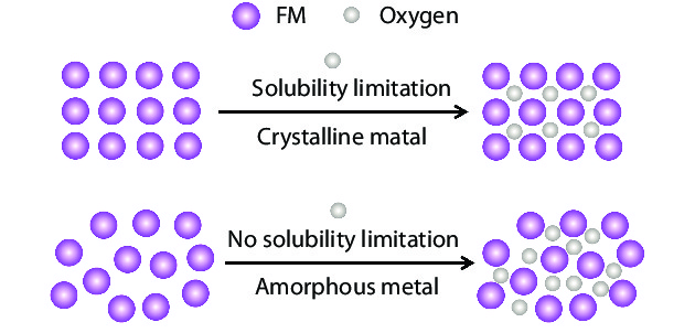
    Fig. 1. (Color online) Schematic diagram for including oxygen in crystalline and amorphous metals. FM denotes ferromagnetic metals.
    (Color online) (a) Schematic diagram for depositing Co–Fe–Ta–B–O thin films. (b)–(j) oxidation process.
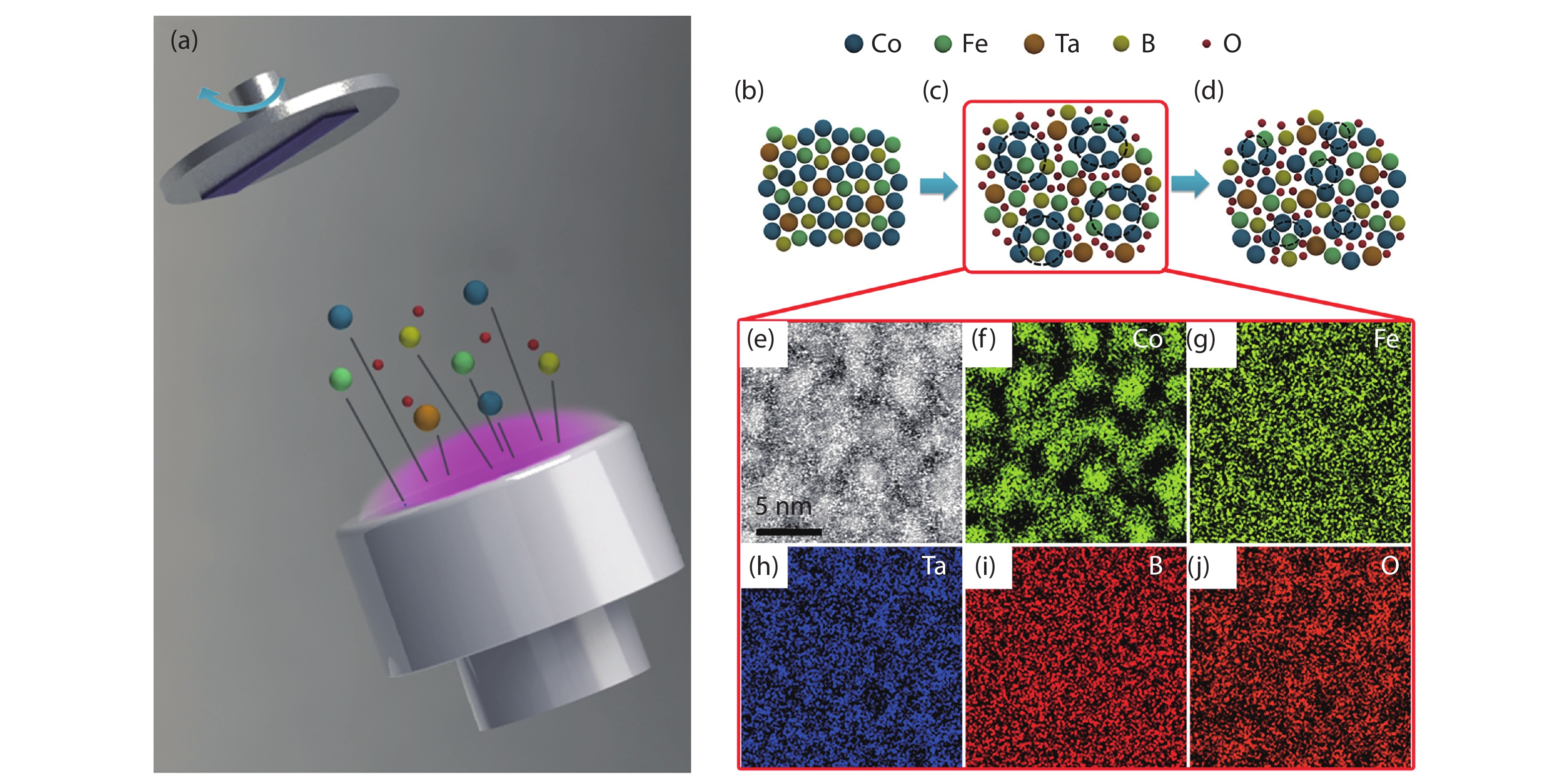
    Fig. 2. (Color online) (a) Schematic diagram for depositing Co–Fe–Ta–B–O thin films. (b)–(j) oxidation process.
    (Color online) High-resolution transmission electron microscopy (HRTEM) images of the CFTBOxsystem (a) CFTB, (b) CFTBO44, and (c) CFTBO46.
    Fig. 3. (Color online) High-resolution transmission electron microscopy (HRTEM) images of the CFTBOxsystem (a) CFTB, (b) CFTBO44, and (c) CFTBO46.
    (Color online) (a) Optical transmittance of the CFTBOx system. (b) Optical bandgap and (c) photoluminescence spectrum of the CFTBO46 thin film.
    Fig. 4. (Color online) (a) Optical transmittance of the CFTBOx system. (b) Optical bandgap and (c) photoluminescence spectrum of the CFTBO46 thin film.
    (Color online) The normalized resistivity ρ/ρ0 as a function of temperature (ρ0 is the room temperature resistivity) for the CFTBOx (16≤ x ≤ 46 at%) thin films. Inset is the plot of ln(ρ/ρ0) versus 1/T1/2 based on the experimental data of the CFTBO46 thin film.
    Fig. 5. (Color online) The normalized resistivity ρ/ρ0 as a function of temperature (ρ0 is the room temperature resistivity) for the CFTBOx (16≤ x ≤ 46 at%) thin films. Inset is the plot of ln(ρ/ρ0) versus 1/T1/2 based on the experimental data of the CFTBO46 thin film.
    (Color online) Magnetic behavior of the CFTBOx (16 ≤ x ≤ 46 at%): (a) Magnetic field dependence of the magnetization (M–H) curves measured at room temperature. (b) Saturation magnetization (Ms) variation with the oxygen contents. (c) Zero-field-cooling (ZFC) and field-cooling (FC) curves measured at an external field of 100 Oe. (d) High-temperature magnetization–temperature (M–T) curve measured for the CFTBO46 thin film at an external field of 100 Oe.
    Fig. 6. (Color online) Magnetic behavior of the CFTBOx (16 ≤ x ≤ 46 at%): (a) Magnetic field dependence of the magnetization (MH) curves measured at room temperature. (b) Saturation magnetization (Ms) variation with the oxygen contents. (c) Zero-field-cooling (ZFC) and field-cooling (FC) curves measured at an external field of 100 Oe. (d) High-temperature magnetization–temperature (MT) curve measured for the CFTBO46 thin film at an external field of 100 Oe.
    (Color online) Schematic diagrams for fabricating p–n (b) and p–n–p heterojunctions based on the CFTBO46 thin film and n-type Si. The Si is heavily doped with phosphorous and has resistivity of order of 10–3 Ω·cm. (c) The I–V curves for the heterojunctions of (a) and (b). The figure was adopted from Ref. [26].
    Fig. 7. (Color online) Schematic diagrams for fabricating p–n (b) and p–n–p heterojunctions based on the CFTBO46 thin film and n-type Si. The Si is heavily doped with phosphorous and has resistivity of order of 10–3 Ω·cm. (c) The IV curves for the heterojunctions of (a) and (b). The figure was adopted from Ref. [26].
    The threshold voltage (Vth) of the p–n heterojunctions increasing with decreasing the resistivity (ρ) of the n-type Si.
    Fig. 8. The threshold voltage (Vth) of the p–n heterojunctions increasing with decreasing the resistivity (ρ) of the n-type Si.
    (Color online) Electric-field control of the ferromagnetism in the CFTBO46 AMS. (a) Schematic diagram of the experimental set-up for applying gate voltages (VG) on the thin films through a drop of ionic liquid. The thickness of an insulating HfO2 layer is about 2 nm. (b) Variation of M–H curves with different VG measured at 300 K.
    Fig. 9. (Color online) Electric-field control of the ferromagnetism in the CFTBO46 AMS. (a) Schematic diagram of the experimental set-up for applying gate voltages (VG) on the thin films through a drop of ionic liquid. The thickness of an insulating HfO2 layer is about 2 nm. (b) Variation of MH curves with different VG measured at 300 K.
    (Color online) (a) HRTEM image of the newly developed CFTBO AMS. (b) Schematic diagrams for the electric-field control of carrier concentrations at different VG. (c) Ms increaisng with both positive and negative VG.
    Fig. 10. (Color online) (a) HRTEM image of the newly developed CFTBO AMS. (b) Schematic diagrams for the electric-field control of carrier concentrations at different VG. (c) Ms increaisng with both positive and negative VG.
    Na Chen, Kaixuan Fang, Hongxia Zhang, Yingqi Zhang, Wenjian Liu, Kefu Yao, Zhengjun Zhang. Amorphous magnetic semiconductors with Curie temperatures above room temperature[J]. Journal of Semiconductors, 2019, 40(8): 081510
    Download Citation