
Na Chen, Kaixuan Fang, Hongxia Zhang, Yingqi Zhang, Wenjian Liu, Kefu Yao, Zhengjun Zhang. Amorphous magnetic semiconductors with Curie temperatures above room temperature[J]. Journal of Semiconductors, 2019, 40(8): 081510
- Journal of Semiconductors
- Vol. 40, Issue 8, 081510 (2019)
Abstract
1. Introduction
The core functions of current-generation computers are to process, communicate and store information. These operations are mainly realized by two fundamental components of microprocessors and hard disks in computers, respectively. Si-based semiconductors are the key materials in microprocessors to enable the control of charges for transmitting and processing data, while ferromagnets provide the spin of electrons to be utilized for storing data on the hard disk. Generally, semiconductivity and ferromagnetism do not coexist in a material. However, it was found that europium chalcogenides showed anomalous optical, magnetic and transport phenomena[
To maintain the most attractive semiconducting properties used in electronic devices, an approach was proposed to introduce magnetic elements into non-magnetic semiconductors for creating new type of magnetic semiconductors (MSs) called diluted magnetic semiconductors (DMSs)[
In contrast to the approach for developing the DMSs, we found a different way to create a new kind of MSs. First, we selected a high Curie-temperature ferromagnetic amorphous alloy (AA) as a host. Second, we introduced oxygen into this AA in a well-controlled manner. AAs are mainly characterized by non-directional and non-saturated metallic bonds. Their disordered atomic structures and unique electronic structures enable them to be nice hosts to include a large quantity of foreign elements[
2. Amorphous magnetic semiconductors
2.1. Metal–semiconductor transition in amorphous alloys
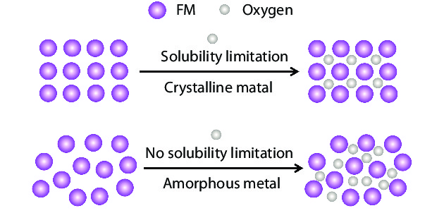
Crystalline metals and AAs behave quite differently as oxygen is introduced into them, respectively (Fig. 1). The solubility of oxygen in a crystalline metal limits the maximal amount of oxygen that enters its lattice structure, whereas no similar limitation exists for oxygen to be included in an AA. Moreover, amorphous materials could access to lower energy states through structural relaxation[
![]()
Figure 1.(Color online) Schematic diagram for including oxygen in crystalline and amorphous metals. FM denotes ferromagnetic metals.
Following the idea of transferring AAs to semiconductors, an alloy system is selected owing to the following three reasons. First, ferromagnetic alloys are preferred in order to obtain MSs with a combination of desirable functionalities. Moreover, the Curie temperatures of the selected alloy systems should be higher than 500 K, which is required for a ferromagnet to work in practical applications[
The Co–Fe–Ta–B–O thin films were deposited by radio frequency (RF) magnetron sputtering with an alloy target under a gas mixture of argon and oxygen[
![]()
Figure 2.(Color online) (a) Schematic diagram for depositing Co–Fe–Ta–B–O thin films. (b)–(j) oxidation process.
The structure of the (Co0.53Fe0.23Ta0.08B0.16)100–xOx (0 ≤ x ≤ 50 at%, abbreviated as CFTBOx hereafter) samples evolved gradually with increasing the oxygen content. High resolution transmission electron microscopy (HRTEM) images and selected area electron diffraction (SAED) patterns were taken for the CFTBOx system, respectively (Fig. 3). The Co53Fe23Ta8B16 AA shows maze-like atomic arrangements typical for amorphous structure (Fig. 3(a)). Its SAED pattern further verifies the formation of a single amorphous phase in the AA (Fig. 3(b)). With increasing the oxygen content above 15 at.%, an amorphous oxide (AO) phase emerges in the CFTBOx thin films. Fig. 3(c) shows the formation of a dual phase nanocomposite in the CFTBO44 thin film, comprising the nanometer-sized AA particles embedded in the AO matrix. Its SAED pattern exhibits two sets of halos (Fig. 3(d)). One arises from the AA nanoparticles (Figs. 3(b) and 3(d)), while the other originates from the AO matrix (Figs. 3(d) and 3(f)). Further increasing the oxygen content to 46 at.% enables the formation of a single AO phase (Fig. 3(e)). The SAED pattern only shows the broad diffraction halo resulting from the single AO phase, which is semiconducting and ferromagnetic[
![]()
Figure 3.(Color online) High-resolution transmission electron microscopy (HRTEM) images of the CFTBOxsystem (a) CFTB, (b) CFTBO44, and (c) CFTBO46.
2.2. Optical, electrical and magnetic properties
Fig. 4(a) shows optical transmittance of the CFTBOx samples at thickness of ~100 nm. With increasing the oxygen content, their optical transmittance increases as well. The optical bandgap of the CFTBO46 thin film is estimated to be about 2.4 eV based on the Tauc plot (Fig. 4(b)). In addition, the thin film exhibits 488 nm-peaked photoluminescence specturm, correpsonding to a photon energy of about 2.5 eV for blue light. This value is in consistent with its optical bandgap energy.
![]()
Figure 4.(Color online) (a) Optical transmittance of the CFTBO
As the charge carrier concentration decreases with the oxygen content, the bandgap of the CFTBOx samples is gradually opened. That is, metal-semiconductor-insulator transitions are induced through this simple oxidization of the ferromagnetic AA. As a result, the resistivity of the CFTBOx samples increases with increasing the oxygen content (Fig. 5). The CFTBO46 thin film exhibits a negative temperature dependence of ln(ρ/ρ0)–1/T1/2 (inset of Fig. 5), characteristic of a semiconductor behavior. Further increasing the oxygen content above 60 at.% makes the CFTBOx samples become insulating.
![]()
Figure 5.(Color online) The normalized resistivity
The magnetic properties of the CFTBOx thin films are shown in Fig. 6. All the thin films are ferromagnetic at the oxygen contents ranging from 16 to 46 at.%. Noted that the saturation magnetization (Ms) of these thin films measured at room temperature increases from 728 to 867 emu/cm3 as the oxygen content increases from 16 to 25 at.%. With further increasing in the oxygen content up to 46 at.%, Ms decreases from 867 to 433 emu/cm3 (Figs. 6(a) and 6(b)). Furthermore, the zero-field cooling (ZFC) curve of the thin film with a low oxygen content of 16 at.% coincides with its field cooling (FC) curve, which is similar to that of the Co–Fe–Ta–B AA without containing oxygen[
![]()
Figure 6.(Color online) Magnetic behavior of the CFTBO
The high-temperature magnetization–temperature (M–T) curve of the CFTBO46 sample shows that its glass transition occurs at about 600 K. The thin film is still ferromagnetic before the glass transition sets in. Therefore, the thin film should have a Curiecurie temperature above 600 K. At about 700 K, the magnetization increases owing to the apparent crystallization, similar to that found in Co16Fe68Hf9B7 alloy[
3. Prototype devices based on the amorphous magnetic semiconductors
3.1. Fabrication of p–n heterojunctions
Based on the above results, it is suggested that the single-phase CFTBO46 thin film is an AMS with a Curie temperature above 600 K. Integrated with a heavily doped n-type Si, p–n and p–n–p heterojunctions were fabricated (Figs. 7(a) and 7(b)). Their current–voltage (I–V) curves are shown in Fig. 7(c). The threshold voltage (Vth) is about 1.6 eV for the p–n heterojunction, whereas no current flows in the p–n–p heterojunctions.
![]()
Figure 7.(Color online) Schematic diagrams for fabricating p–n (b) and p–n–p heterojunctions based on the CFTBO46 thin film and n-type Si. The Si is heavily doped with phosphorous and has resistivity of order of 10–3 Ω·cm. (c) The
The voltage difference (VD) built inside the p–n heterojunction can be described by the following equation:
In the equation, q denotes the electron charge, Ei2 and Ei1 denote the Fermi energy levels of the intrinsic states of Si and CFTBOx thin films, respectively, k denotes the Boltzmann constant, T denotes the temperature, NA and ND denote the carrier concentrations of the CFTBO46 thin film and n-type Si, respectively, ni1 and ni2 denote the intrinsic carrier concentrations of the CFTBOx and Si, respectively. Assuming that Ei2, Ei1, NA, ni1 and ni2 are constants, VD increases with ND. A higher ND indicates a lower ρ for n-type Si. Meanwhile, Vth of the p–n heterojunction is required to be larger than VD for the forward conduction current to flow. As a consequence, Vth decreases with increasing ρ of the n-type Si as shown in Fig. 8.
![]()
Figure 8.The threshold voltage (
3.2. Electric-field control of the ferromagnetism
Magnetic properties of ferromagnets are thought to be their inherent characteristics of the response to external magnetic fields. These magnetic properties are difficult to be changed once they are prepared[
Fig. 9(a) shows a schematic diagram of a field effecttransistor (FET) with HfO2 (2 nm)/ CFTBO46 (25 nm)/Au/Cr/Si heterostructure. Through an ionic liquid (DEME-TFSI) dropped on the surface of the CFTBO46 thin film, the gate voltage (VG) is applied by forming an electric double layer (EDL) to achieve a large variation in its carrier density. Such a method has proven to be effective for realizing the stable modulation of carrier densities even when the gate voltage is removed[
![]()
Figure 9.(Color online) Electric-field control of the ferromagnetism in the CFTBO46 AMS. (a) Schematic diagram of the experimental set-up for applying gate voltages (
3.3. Development of an intrinsic magnetic semiconductor
The present CFTBO46 MS is a p-type semiconductor. It is found that most of the existing AOs are n-type and are notoriously doped in p-type. Moreover, the control of their electrical conduction type remains a challenge. The conduction type of the AOs is determined by their local atomic configuration and the valence states of the involved metal cations[
To alter the conduction type of the present Co–Fe–Ta–B–O system, we modified the relative atomic ratios of Co and Fe in the system. As shown in Fig. 10(a), a new single-phase AO is developed. Its HRTEM image presents a maze-like pattern characterizing single-phase amorphous structure formed in the Co–Fe–Ta–B–O thin film. The electric-field control of its ferromagnetism is different from that of the p-type CFTBO46 MS. No matter whether VG is positive or negative, its Ms increases. It is suggested that the newly developed Co–Fe–Ta–B-O sample could be an intrinsic MS. Based on this intrinsic MS, we may use VG to control its electrical conduction type of the different parts within the material, which would form a p–n junction at the interface between the different parts. To the best of our knowledge, this should be the first demonstration of an intrinsic MS. Meanwhile, the conduction type of this intrinsic MS can be tuned to be n-type or p-type by using an external electric field.
![]()
Figure 10.(Color online) (a) HRTEM image of the newly developed CFTBO AMS. (b) Schematic diagrams for the electric-field control of carrier concentrations at different
4. Conclusions and future perspectives
A new type of AMSs was developed by oxidizing originally ferromagnetic AAs. These AMSs showed high Curie temperatures well above room temperature. Based on them, prototype p–n heterojunctions were fabricated. Owing to the interplay between the holes and local magnetic moments, the electric-field control of ferromagnetism was realized at room temperature in these AMSs. The realization of high-Curie-temperature AMSs offers an opportunity to create next generation spintronic devices such as spin-diodes and spin-field effect transistors. The carrier mobility of amorphous materials is known to be very low. Therefore, these AMSs could not be good channel materials to be used in semiconductor-based devices. However, new phenomena may emerge at the interface between two AMSs if they are integrated together to form a field effect transistor. Therefore, furthering our understanding of the possible unprecedented interface effects may help to design and develop high performance spintronic devices based on these AMSs.
Future research subjects related to this new type of AMSs will be focused on the following three aspects:
(1) Both p-type and n-type AMSs are important for fabricating magnetic p-n diodes or spintronic transistors. The control of electrical conduction type in these AMSs should be possible through the compositional tuning based on the Co–Fe–Ta–B–O system. In this way, n-type AMSs could be developed to show high Curie temperature well above room temperature.
(2) New kinds of high performance MSs could be developed based on various ferromagnetic AAs. For example, the Co–Fe–Nb–B system is similar to the Co–Fe–Ta–B system. Oxidizing the Co–Fe–Nb–B AAs may lead to the formation of new AMSs with different properties. In addition to oxygen, nitrogen or sulfur can be used as elemental additions to transfer a ferromagnetic AA to AMSs. On the other hand, the precise characterization of the amorphous structure remains elusive from both theoretical and experimental aspects. A spectrum of behavior from ferromagnetic metal to insulator is realized in one Co–Fe–Ta–B–O system via continuously compositional adjustability. Hence, the amorphous structure can be manipulated in a well controllable manner, leading to tunable optical, electrical and magnetic properties over a wide range. This will help to build a reliable relationship between the amorphous structure and properties of these amorphous materials.
(3) New design concepts and device structures should be proposed for this new type of AMSs, aiming to combine logic functionalities and information storage capabilities in a single device through manipulating the spin and charge simultaneously. This will facilitate the development of next-generation spintronic devices with low power, rapid response and high storage density.
Acknowledgments
We thank Prof. Cheng Song, Prof. Xiangrong Wang and Prof. Xiaozhong Zhang for profound discussions and comments. This work is sponsored by the National Key R&D Program of China (Grant No. 2017YFB0405704) and the National Natural Science Foundation of China (Grant No. 51471091).
References
[1] F Holtzberg, T R McGuire, S Methfessel et al. Effect of electron concentration on magnetic exchange interactions in rare earth chalcogenides. Phys Rev Lett, 13, 18(1964).
[2] T Kasuya, A Yanase. Anomalous transport phenomena in Eu-chalcogenide alloys. Rev Mod Phys, 40, 684(1968).
[3] S Methfessel. Potential applications of magnetic rare earth compounds. IEEE Trans Mag, 1, 144(1965).
[4]
[5] T Dietl, H Ohno. Dilute ferromagnetic semiconductors: physics and spintronic structures. Rev Mod Phys, 86, 187(2014).
[6] H Ohno. Making nonmagnetic semiconductors ferromagnetic. Science, 281, 951(1998).
[7] H Ohno, A Shen, F Matsukura et al. (Ga,Mn)As: A new diluted magnetic semiconductor based on GaAs. Appl Phys Lett, 69, 363(1996).
[8] H Munekata, H Ohno, Molnár S von et al. Diluted magnetic III–V semiconductors. Phys Rev Lett, 63, 1849(1989).
[9] L Chen, X Yang, F H Yang et al. Enhancing the Curie temperature of ferromagnetic semiconductor (Ga,Mn)As to 200 K via nanostructure engineering. Nano Lett, 11, 2584(2011).
[10] Y Matsumoto, M Murakami, T Shono et al. Room-temperature ferromagnetism in transparent transition metal-doped titanium dioxide. Science, 291, 854(2001).
[11] F Pulizzi, S Chambers. Is it really intrinsic ferromagnetism. Nat Mater, 9, 956(2010).
[12] L Chen, S Yan, P F Xu et al. Low-temperature magnetotransport behaviors of heavily Mn-doped (Ga,Mn)As films with high ferromagnetic transition temperature. Appl Phys Lett, 95, 182505(2009).
[13] F Pulizzi, N Samarth. A model ferromagnetic semiconductor. Nat Mater, 9, 955(2010).
[14] H Ohno. A window on the future of spintronics. Nat Mater, 9, 952(2010).
[15] X L Wang, H L Wang, D Pan et al. Robust manipulation of magnetism in dilute magnetic semiconductor (Ga,Mn)As by organic molecules. Adv Mater, 27, 8043(2015).
[16] . More than just room temperature. Nat Mater, 9, 951(2010).
[17] S H Nie, Y Y Chin, W Q Liu et al. Ferromagnetic interfacial interaction and the proximity effect in a Co2FeAl/(Ga,Mn)As bilayer. Phys Rev Lett, 111, 027203(2013).
[18] T Dietl. A ten-year perspective on dilute magnetic semiconductors and oxides. Nat Mater, 9, 965(2010).
[19] X Z Yu, H L Wang, D Pan et al. All zinc-blende GaAs/(Ga,Mn)As core-shell nanowires with ferromagnetic ordering. Nano Lett, 13, 1572(2013).
[20] J H Zhao. Is it possible to create magnetic semiconductors that work at room temperature. Chin Sci Bull, 61, 1401(2016).
[21]
[22] L M Hoistad, S Lee. The Hume-Rothery electron concentration rules and second moment scaling. J Am Chem Soc, 113, 8216(1991).
[23]
[24] N Chen, Y Q Zhang, K F Yao. Transparent magnetic semiconductors from ferromagnetic amorphous alloys. Acta Phys Sin, 66, 176113(2017).
[25] N Chen, H P Li, A Hirata et al. Transparent magnetic semiconductor with embedded metallic glass nano-granules. Mater Design, 132, 208(2017).
[26] W J Liu, H X Zhang, J A Shi et al. A room-temperature magnetic semiconductor from a ferromagnetic metallic glass. Nat Commun, 7, 13497(2016).
[27] A Inoue. Stabilization of metallic supercooled liquid and bulk amorphous alloys. Acta Mater, 48, 279(2000).
[28] W L Johnson. Bulk glass-forming metallic alloys: science and technology. MRS Bull, 24, 42(1999).
[29] A L Greer. Metallic glasses. Science, 267, 1947(1995).
[30] W H Wang, C Dong, C H Shek. Bulk metallic glasses. Mater Sci Eng R, 44, 45(2004).
[31] M W Chen. A brief overview of bulk metallic glasses. NPG Asia Mater, 3, 82(2011).
[32] J M D Coey, M Venkatesan, C B Fitzgerald. Donor impurity band exchange in dilute ferromagnetic oxides. Nat Mater, 4, 173(2005).
[33] A Inoue, B L Shen, H Koshiba et al. Ultra-high strength above 5000 MPa and soft magnetic properties of Co–Fe–Ta–B bulk glassy alloys. Acta Mater, 52, 1631(2004).
[34] A Inoue, B L Shen, H Koshiba et al. Cobalt-based bulk glassy alloy with ultrahigh strength and soft magnetic properties. Nat Mater, 2, 661(2003).
[35] P Sharma, H Kimura, A Inoue. Observation of unusual magnetic behavior: spin reorientation transition in thick Co–Fe–Ta–B glassy films. J Appl Phys, 100, 083902(2006).
[36] P Sharma, H Kimura, A Inoue et al. Temperature and thickness driven spin-reorientation transition in amorphous Co–Fe–Ta–B thin films. Phys Rev B, 73, 052401(2006).
[37] M S Lucas, W C Bourne, A O Sheets et al. Nanocrystalline Hf and Ta containing FeCo based alloys for high frequency applications. Mater Sci Eng B, 176, 1079(2011).
[38] J P Pellegren, V M Sokalski. Thickness and interface-dependent crystallization of CoFeB alloy thin films. IEEE Trans Magn, 51, 3400903(2015).
[39] S D Bader, S S P Parkin. Spintronics. Ann Rev Condens Matter Phys, 1, 71(2010).
[40] H Ohno, D Chiba, F Matsukura et al. Electric-field control of ferromagnetism. Nature, 408, 944(2000).
[41] C Song, B Cui, F Li et al. Recent progress in voltage control of magnetism: materials, mechanisms, and performance. Prog Mater Sci, 87, 33(2017).
[42] I Žutić, J Fabian, Sarma S Das. Spintronics: fundamentals and applications. Rev Mod Phys, 76, 323(2004).
[43] F Hellman, A Hoffmann, Y Tserkovnyak et al. Interface-induced phenomena in magnetism. Rev Mod Phys, 89, 025006(2017).
[44] D D Awschalom, M E Flatté. Challenges for semiconductor spintronics. Nat Phys, 3, 153(2007).
[45] M Weisheit, S Fähler, A Marty et al. Electric field-induced modification of magnetism in thin-film ferromagnets. Science, 315, 349(2007).
[46] B Cui, C Song, H J Mao et al. Manipulation of electric field effect by orbital switch. Adv Funct Mater, 26, 753(2016).
[47] B Cui, C Song, G Y Wang et al. Reversible ferromagnetic phase transition in electrode-gated manganites. Adv Funct Mater, 24, 7233(2014).
[48] Y Yamada, K Ueno, T Fukumura et al. Electrically induced ferromagnetism at room temperature in cobalt-doped titanium dioxide. Science, 332, 1065(2011).
[49] Y Q Zhang, S F Zhao, C Song et al. Electric-field control of ferromagnetism in a Co–Fe–Ta–B amorphous alloy. Mater Design, 143, 65(2018).
[50] S Zhang, Y G Zhao, X Xiao et al. Giant electrical modulation of magnetization in Co40Fe40B20/ Pb(Mg1/3Nb2/3)0.7Ti0.3O3(011) heterostructure. Sci Rep, 4, 3727(2014).
[51] Y T Liu, G Agnus, S Ono et al. Ionic-liquid gating of perpendicularly magnetised CoFeB/MgO thin films. J Appl Phys, 120, 023901(2016).
[52] M Nakano, K Shibuya, D Okuyama et al. Collective bulk carrier delocalization driven by electrostatic surface charge accumulation. Nature, 487, 459(2012).
[53] S Narushima, H Mizoguchi, K Shimizu et al. A p-type amorphous oxide semiconductor and room temperature fabrication of amorphous oxide p–n heterojunction diodes. Adv Mater, 15, 1409(2003).

Set citation alerts for the article
Please enter your email address
© Copyright 2018-2021 | Chinese Laser Press. All Rights Reserved 沪ICP备15018463号-20