• Chinese Optics Letters
  • Vol. 18, Issue 9, 092501 (2020)
Jingzhan Shi, Fangzheng Zhang*, De Ben, and Shilong Pan
Author Affiliations
  • Key Laboratory of Radar Imaging and Microwave Photonics, Ministry of Education, Nanjing University of Aeronautics and Astronautics, Nanjing 210016, China
  • show less
    DOI: 10.3788/COL202018.092501 Cite this Article Set citation alerts
    Jingzhan Shi, Fangzheng Zhang, De Ben, Shilong Pan. Photonic-assisted single system for microwave frequency and phase noise measurement[J]. Chinese Optics Letters, 2020, 18(9): 092501 Copy Citation Text show less

    Abstract

    We propose a photonic-assisted single system for measuring the frequency and phase noise of microwave signals in a large spectral range. Both the frequency and phase noise to be measured are extracted from the phase difference between the signal under testing and its replica delayed by a span of fiber and a variable optical delay line (VODL). The system calibration, frequency measurement, and phase noise measurement are performed by adjusting the VODL at different working modes. Accurate frequency and phase noise measurement for microwave signals in a large frequency range from 5 to 50 GHz is experimentally demonstrated.

    Frequency and phase noise are important parameters of microwave signals. Both frequency measurement and phase noise measurement have been applied to recognize RF signals in electronic warfare (EW) applications[1,2]. In view of the fact that microwave photonic technology has a great potential for use in overcoming the bandwidth limitation and enhancing the performance of electronic systems[35], many photonic-assisted approaches have been proposed to characterize RF signals in a wide spectral range and having an ultra-low phase noise[68]. The basic principle of photonic-assisted microwave frequency measurement is to map the frequency of the signal under test (SUT) to a parameter that is easily observed, such as power, time, space, and phase slope[912]. For example, microwave frequency measurement with an error less than 200 MHz was done by frequency-to-power mapping in Ref. [9], and a frequency measurement range from 5 to 67 GHz was achieved by frequency-to-phase-slope mapping with a microwave photonic in-phase and quadrature (I/Q) mixer[12]. On the other hand, high-sensitivity phase noise measurement of microwave signals can be implemented by the photonic-assisted frequency-detection method[1320], in which the phase noise is derived from the phase difference between the SUT and its delayed replica. The low-loss optical fiber is naturally an ideal delay line[13,14], providing a large amount of time delay to enhance the measurement sensitivity. Previously, a 2 km length single mode fiber (SMF) enabled a phase noise measurement sensitivity as high as 134dBc/Hz at 10 kHz[15]. In addition to the use of an optical fiber delay line, photonic-assisted phase controlling and frequency mixing were also applied in such systems to overcome the bandwidth limitation of electrical devices and hence to broaden the spectral range that can be measured[1621]. In Ref. [21], we have proposed a phase noise measurement system with a large measurement range from 5 to 50 GHz by applying an all-optical microwave I/Q mixer that is implemented by a cascaded Mach–Zehnder modulator (MZM) and a polarization modulator (PolM). To deal with the direct-current (dc) interference and I/Q mismatch of the mixer, a simple calibration method using a variable optical delay line (VODL) is also proposed.

    The previous photonic-assisted microwave frequency measurement and phase noise measurement are physically isolated from each other, i.e., the system can only to execute one function. In EW applications, to improve the probability of detection, it is desirable to jointly estimate the frequency and the phase noise of the received RF signals. In this Letter, based on our previous work in Ref. [21], a photonic-assisted system is proposed to measure both the frequency and phase noise of single-tone microwave signals in a large spectral range. To the best of our knowledge, this is the first time that photonic-assisted microwave frequency measurement and phase noise measurement are implemented in a single system, which is highly desirable for fabricating compact and multi-functional EW devices.

    Figure 1 shows the schematic diagram of the proposed system in which several illustrative spectra of the optical signals at different positions are also provided. The SUT s(t)=Vscos[2πfst+φs(t)] is divided into two parts, where Vs, fs, and φs(t) are the amplitude, frequency, and phase fluctuation of the SUT, respectively. At a phase modulator (PM), one part of the SUT modulates the phase of a continuous-wave (CW) light emitted from a laser diode (LD) that has an amplitude Ec, a frequency fc, and a phase fluctuation φc(t). The optical field at the output of the PM is where β is the modulation index of the phase modulation.

    Schematic diagram of the microwave photonic system for wideband microwave frequency and phase noise measurement. LD: laser diode; PM: phase modulator; SMF: single-mode fiber; VODL: variable optical delay line; PolM: polarization modulator; SUT: signal under test; OBPF: optical bandpass filter; OC: optical coupler; Pol: polarizer; PD: photodiode; ADC: analog-to-digital converter; DSP: digital signal processing.

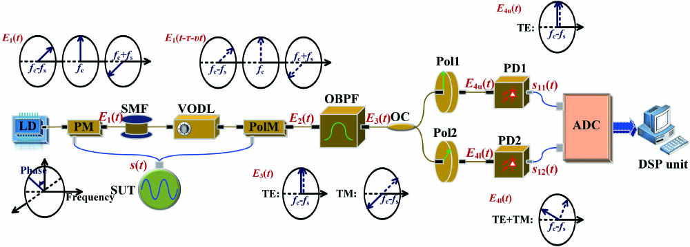
    Figure 1.Schematic diagram of the microwave photonic system for wideband microwave frequency and phase noise measurement. LD: laser diode; PM: phase modulator; SMF: single-mode fiber; VODL: variable optical delay line; PolM: polarization modulator; SUT: signal under test; OBPF: optical bandpass filter; OC: optical coupler; Pol: polarizer; PD: photodiode; ADC: analog-to-digital converter; DSP: digital signal processing.

    The phase-modulated optical signal is delayed by a span of SMF followed by a VODL. Assuming the time delay provided by the SMF is τ and the varying speed of the VODL is ν, the optical signal after delay would be E1(tτνt). The delayed optical signal is modulated by the other part of the SUT at a PolM, which supports transverse electric (TE) and transverse magnetic (TM) fields with opposite phase modulation indices, i.e., γ and γ, respectively. The optical field at the output of the PolM can be expressed as where ϕ is set to be π/2 by adjusting the bias of the PolM.

    Then, the polarization-modulated optical signal is sent to an optical bandpass filter (OBPF) to select the frequency components at fcfs. The optical signal at the output of the OBPF is split into two branches by an optical coupler (OC). In the upper branch of the OC, a polarizer (Pol1) is applied to select the TE field as expressed by

    In the lower branch, another polarizer (Pol2), of which the polarization direction has an angle of π/4 to that of the TE or TM field, is used to perform vector addition of the TE and TM fields. The obtained optical signal is

    Following the two polarizers, a pair of low-speed photodiodes (PD1 and PD2) are used for optical-to-electrical conversion. The electrical voltages at the outputs of PD1 and PD2 are where R1 and R2 are the responsivities of PD1 and PD2, respectively, ZL is the input impedance of the PDs, the phase term ψ(t,ν)=2πfs(τ+νt)+φs(t)φs(tτνt) contains the frequency and phase fluctuation of the SUT, s10 and s20 are defined as dc interferences, and A1/A2 is the amplitude imbalance of the I/Q mixer. Both the dc interferences and the amplitude imbalance are hard to calculate because the related parameters (Ec, β, γ, R1, and R2) are difficult to be measured accurately. Here, we use a simple calibration method to solve this problem. If we tune the time delay of the VODL with a constant speed (ν is a non-zero constant), both s11(t) and s12(t) are two sinusoidal functions versus time. The dc biases of the two sinusoidal functions are equal to s10 and s20, respectively, and the amplitudes of them are equal to A1 and A2, respectively. Thus, si0 and Ai(i=1,2) can be acquired by where M[s1i(t)] and N[s1i(t)] represent the maximum and the minimum of s1i(t) within a time duration longer than 1/fsν. Then, the phase term ψ(t,ν) can be derived from the following equation:

    Once the phase term ψ(t,ν) is obtained, the frequency of the SUT can be estimated based on the phase slope, i.e., where slope[ψ(t,ν)] represents the slope of ψ(t,ν) with respect to time, which is calculated through linear least-square fitting, i.e., where ψ1,ψ1,,ψN are the phase values corresponding to the time at t1,t2,,tN, respectively. According to Eq. (7), the phase fluctuation under a specific time delay provided by the VODL (ν=0) can be obtained, based on which the phase noise of the SUT can be calculated by where Sφs(fm) and Sψ(fm) are the power spectral density (PSD) of the phase fluctuation φs(t) and the PSD of the phase term ψ(t,0), respectively. Considering that ψ(t,0)=2πfsτ+φs(t)φs(tτ) and the time delay τ is a constant, the PSD of ψ(t,0) is equal to the PSD of φs(t)φs(tτ) at a non-zero frequency, i.e., Sψ(fm)=[φs(t)φs(tτ)]PSD for fm0.

    The principle of the proposed system indicates that, without reconfiguring the system structure, calibration of the parameters and frequency measurement are achieved by operating the VODL in a scanning mode, and phase noise measurement is implemented with the VODL providing a specific time delay. This property makes a significant improvement over the single-function system in Ref. [21]. In addition, the system in Ref. [21] uses an MZM that is biased at the quadrature point to construct the I/Q mixer. In this work, the MZM is replaced by a PM, which is free from adjustment of the dc bias.

    To test the performance of the proposed system, a proof-of-concept experiment is conducted. The SUT is generated by a microwave signal generator (Agilent E8257D). The SUT is split into two equal parts by a 50:50 power divider (3 dB bandwidth: 50 GHz). The optical carrier emitted from an LD (TeraXion Inc., wavelength: 1550.12 nm) is modulated by one part of the SUT at a PM (Eospace Inc., 3 dB bandwidth: 40 GHz). A span of SMF (length: 2 km) followed by a VODL (General Photonics, time delay range: 0–660 ps) provides the variable time delay. The delayed optical signal is modulated by the other part of the SUT at a PolM (Versawave Inc., bandwidth: 40 GHz, extinction ratio: >20dB). The polarization-modulated signal is filtered by an OBPF (Yenista Inc., edge roll-off: 500 dB/nm) and then is split into two channels by an OC. In each channel, a polarizer (extinction ratio: >20dB) and a low-speed PD (bandwidth: 150 MHz) are used for polarization adjustment and optical-to-electrical conversion. The obtained electrical signals are sampled by a two-channel ADC (National Instruments Inc., sampling rate: 204.8 kSa/s).

    First, the frequency of the SUT is tuned to 26.5 GHz. The spectrum of the optical signal at the output of the PolM, the response of the OBPF, and the spectrum of the optical signal at the output of the OBPF are plotted in Fig. 2. It can be seen that the power of the desired frequency component is 27 dB higher than that of the residual undesired component after the OBPF. When the time delay of the VODL is tuned with a constant speed of 128 ps/s, the waveforms of the signals at the output of the PDs are shown in Fig. 3(a). According to Eq. (6), the dc interferences in the upper and lower channels are 16.1 mV and 28.3 mV, respectively, and the amplitude imbalance is 0.766. Based on Eq. (7), the phase term ψ(t,128ps/s) is derived, as shown in Fig. 3(b). The slope of ψ(t,128ps/s) with respect to time is calculated according to Eq. (9). Figure 3(c) shows the estimated phase slope when the value of N in Eq. (9) is 10. It can be seen that the estimated phase slope is 21.37 rad/s, corresponding to an estimated frequency of 26.571 GHz. Compared with the real value, the frequency measurement has an error of 71 MHz.

    Optical spectrum at the output of the PolM, the response of the OBPF, and the spectrum at the output of the OBPF.

    Figure 2.Optical spectrum at the output of the PolM, the response of the OBPF, and the spectrum at the output of the OBPF.

    Frequency measurement of a 26.5 GHz signal. (a) Waveforms of the voltages at the output of the PDs; (b) phase term ψ(t,128 ps/s); (c) estimated phase slope.

    Figure 3.Frequency measurement of a 26.5 GHz signal. (a) Waveforms of the voltages at the output of the PDs; (b) phase term ψ(t,128ps/s); (c) estimated phase slope.

    Then, the time delay of the VODL is fixed. Based on the obtained phase term ψ(t,0), the phase noise of the 26.5 GHz signal is calculated according to Eq. (10). The result is shown in Fig. 4. As a comparison, the measurement result by a commercial phase noise analyzer (R&S, FSWP50, number of correlations: 100) and the phase noise floor of the phase noise analyzer[22] are also plotted in Fig. 4. It can be seen that the phase noise at offset frequencies larger than 1 kHz measured by the proposed system agrees well with that measured by the commercial phase noise analyzer. Meanwhile, the obvious deviation at offset frequencies less than 1 kHz is caused by the limited sensitivity at low offset frequencies of the proposed system, which is a common problem suffered by the frequency-detection-based phase noise analyzers[23]. In order to evaluate the phase noise measurement sensitivity, the noise floor of the proposed system is measured by replacing the 2 km SMF with an optical attenuator having the same insertion loss[1517,20,21,24,25]. The measured noise floor is also plotted in Fig. 4. As can be seen, the phase noise measurement sensitivity of the established system is 102dBc/Hz at 1 kHz and 133dBc/Hz at 10 kHz, respectively. To further improve the phase noise measurement sensitivity, the cross-correction method as demonstrated in Refs. [24] and [25] can be applied, based on which the phase noise floor can be reduced to as low as 156.2dBc/Hz at 10 kHz[24].

    Phase noise measurement results of the 26.5 GHz signal by the proposed system and a commercial phase noise analyzer, and noise floor of the proposed system and R&S FSWP50.

    Figure 4.Phase noise measurement results of the 26.5 GHz signal by the proposed system and a commercial phase noise analyzer, and noise floor of the proposed system and R&S FSWP50.

    Compared with current electrical systems, one advantage of the photonic-assisted measurement is a large operation bandwidth. To test this property, the frequency and phase noise of RF signals tuned from 5 to 50 GHz are measured. For frequency measurement, Fig. 5(a) shows the averaged error of 100 repeated measurements of a single frequency, which is tuned with a step of 1 GHz. It can be seen that the errors are kept within ±150MHz in the whole range. The phase noises of the RF signals tuned from 5 to 50 GHz with a step of 5 GHz are measured by the proposed system. Figure 5(b) shows the measured phase noise at 1 kHz and 10 kHz offset frequencies obtained by averaging 10 repeated measurement results, and the corresponding error bars. As a comparison, the phase noise measured by the commercial phase noise analyzer is also plotted in Fig. 5(b). As can be seen, the deviations between the measured phase noises at a 10 kHz offset frequency for each carrier frequency are less than 5 dB in the whole frequency range. Meanwhile, the deviations between the measured results at a 1 kHz offset frequency are relatively larger because of the limited sensitivity at low offset frequencies, especially for the 5 GHz and the 10 GHz signals that have low phase noises. In Fig. 5(b), the error bars are kept within ±3dB, which confirms that the phase noise measurement has a good stability. It should also be mentioned that the lower limit of the frequency measurement range is related to the edge roll-off of the OBPF. In our experiment, when the measurement frequency is lower than 5 GHz, the undesired modulation sidebands cannot be totally removed by the OBPF, making the measurement unreliable. A possible solution to this problem is to implement frequency upconversion[18] before measuring the phase noise with the proposed system.

    (a) Frequency measurement and (b) phase noise measurement results of RF signals tuned from 5 to 50 GHz.

    Figure 5.(a) Frequency measurement and (b) phase noise measurement results of RF signals tuned from 5 to 50 GHz.

    In conclusion, we have proposed and demonstrated a photonic-assisted system to measure both the frequency and the phase noise of single-tone microwave signals in a wide spectral range. Experimental results show that the proposed system can accurately measure the frequency and the phase noise of microwave signals in a large frequency range from 5 to 50 GHz. In the whole range, the frequency measurement errors are demonstrated to be less than 150 MHz, and the phase noise measurement errors at a 10 kHz offset frequency are within ±3dB. The proposed system can find applications in EW systems for broadband RF signal recognition and classification.

    References

    [1] P. W. East. IET Radar Sonar Navigat., 6, 112(2012).

    [2] M. Nouri, M. Mivehchy, M. F. Sabahi. Electron. Lett., 53, 808(2017).

    [3] G. Yang, W. Zou, Y. Yuan, J. Chen. Chin. Opt. Lett., 16, 030601(2018).

    [4] J. Yang, S. Li, X. Xiao, D. Wu, X. Xue, X. Zheng. Chin. Opt. Lett., 16, 060605(2018).

    [5] F. Zhang, Q. Guo, Y. Zhang, Y. Yao, P. Zhou, D. Zhu, S. Pan. Chin. Opt. Lett., 15, 112801(2017).

    [6] J. Yao. J. Lightwave Technol., 27, 314(2009).

    [7] S. Pan, J. Yao. J. Lightwave Technol., 35, 3498(2016).

    [8] X. Zou, B. Lu, W. Pan, L. Yan, A. Stöhr, J. Yao. Laser Photon. Rev., 10, 711(2016).

    [9] H. Chi, X. H. Zou, J. P. Yao. IEEE Photon. Technol. Lett, 20, 1249(2008).

    [10] J. Shi, F. Zhang, D. Ben, S. Pan. J. Lightwave Technol., 38, 2171(2020).

    [11] X. Zou, W. Li, W. Pan, L. Yan, J. Yao. IEEE Trans. Microwave Theory Technol., 61, 3470(2013).

    [12] J. Shi, F. Zhang, D. Ben, S. Pan. IEEE Trans. Microwave Theory Technol., 67, 544(2018).

    [13] P. Salzenstein, J. Cussey, H. Tavernier, P. Salzenstein, G. Sauvage, L. Larger, E. Rubiola. Acta Phys. Pol. A, 112, 1107(2007).

    [14] E. Rubiola, E. Salik, S. Huang, N. Yu, L. Maleki. J. Opt. Soc. Am. B, 22, 987(2005).

    [15] J. Shi, F. Zhang, S. Pan. IEEE Trans. Microwave Theory Technol., 66, 4306(2018).

    [16] D. Zhu, F. Zhang, P. Zhou, S. Pan. Opt. Lett., 40, 1326(2015).

    [17] F. Zhang, D. Zhu, S. Pan. Electron. Lett., 51, 1272(2015).

    [18] W. Wang, J. Liu, H. Mei, W. Sun, N. Zhu. J. Lightwave Technol., 34, 3425(2016).

    [19] N. Kuse, M. E. Fermann. Sci. Rep., 7, 2847(2017).

    [20] F. Zhang, J. Shi, S. Pan. Opt. Express, 25, 22760(2017).

    [21] J. Shi, F. Zhang, D. Ben, S. Pan. J. Lightwave Technol., 36, 4319(2018).

    [22]

    [23] Y. Sakuta, H. Mino, Y. Sekine. Electron. Comm. Jpn. Pt. II, 84, 64(2001).

    [24] Z. Fan, Q. Qiu, J. Su, T. Zhang, N. Yang. IEEE Photon. J., 10, 5500509(2018).

    [25] Z. Fan, Q. Qiu, J. Su, T. Zhang, Y. Lin. Opt. Lett., 44, 1992(2019).

    Jingzhan Shi, Fangzheng Zhang, De Ben, Shilong Pan. Photonic-assisted single system for microwave frequency and phase noise measurement[J]. Chinese Optics Letters, 2020, 18(9): 092501
    Download Citation