
Zhiyi Xuan, Qingquan Liu, Zhuangzhuang Cui, Songlei Huang, Bo Yang, Chenlu Li, Shaowei Wang, Wei Lu. On-chip short-wave infrared multispectral detector based on integrated Fabry–Perot microcavities array[J]. Chinese Optics Letters, 2022, 20(6): 061302
- Chinese Optics Letters
- Vol. 20, Issue 6, 061302 (2022)
Abstract
1. Introduction
Spectroscopy information is widely used to identify different matter and has a lot of applications, such as sensors[
In this work, we propose a new SWIR multispectral detector chip by monolithically integrating a Fabry–Perot (FP) microcavities array on an InGaAs FPA, which can acquire multiple narrowband spectral signals itself with an ultra-compact footprint. Meanwhile, it has no moving parts and is portable and stable.
2. Experiment
We proposed and developed a new type of wavelength division device based on the integrated narrow bandpass filters[
Sign up for Chinese Optics Letters TOC. Get the latest issue of Chinese Optics Letters delivered right to you!Sign up now
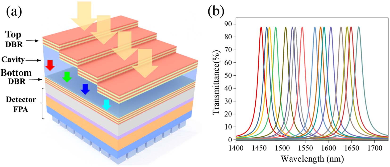
Figure 1(a) shows the schematic diagram of a monolithic integrated multispectral InGaAs detector. The detector chip comprises two parts: one is the pixels InGaAs FPA, whose origin spectral response range is from 900 to 1700 nm; the other is the monolithic integrated FP microcavities array, which is directly fabricated on the backside of the InGaAs FPA. The film stacks of the FP microcavity can be described as , which can be designed in detail according to our previous work[
![]()
Figure 1.(a) Schematic diagram of the FP microcavities array directly integrated on an InGaAs detector. (b) Simulated spectra of 16 FP microcavities array directly integrated on the InGaAs FPA.
The fabrication process is illustrated in Fig. 2. The Si and layers are deposited on the backside of the InGaAs detector by using an electron beam evaporation system (Leybold ARES1110) with vacuum of (1 mbar = 100 Pa) and temperature of 100°C, where the evaporation speed for is 48 nm/min, and for Si is 12.6 nm/min. The bottom DBR stacks and cavity layer of 2.37L are deposited firstly. Then, the cavity layer is processed with combinatorial etching processes. Sixteen cavities with different thicknesses are fabricated with only four times of UV lithography (MJB4, SUSS Mask aligner05080104) and inductively coupled plasma (ICP, Oxford PlasmaPro System 100) etching process. The two gases used for etching were argon (Ar) and trifluoromethane () with a flow rate ratio of 1:3. The radio frequency (RF) power and ICP power were set as 50 W and 80 W, respectively. In addition to the combinatorial etching process, the FP microcavities array can also be realized by using combinatorial deposition processes[
![]()
Figure 2.Fabrication process of on-chip InGaAs multispectral detector. (a) The InGaAs FPA. (b) The bottom DBR and cavity layer are deposited on the InGaAs FPA. (c) The cavity layer is processed with UV lithography and ICP etching. (d) The top DBR is deposited on the processed cavity layer and forms 16 different FP microcavities.
3. Results and Discussion
After the monolithic integrated process, the multispectral detector chip is bonded with ROIC [Fig. 3(a)]. The total footprint of the fabricated 16-channel multispectral detector chip is about , which is minimum and much smaller than the size of conventional infrared multispectral system. The spectral response of the fabricated 16-channel multispectral detector is measured by a monochromator with a collimator, as shown in Fig. 4(a). Meanwhile, the same type of standard InGaAs FPA is measured by the same system as a comparison. The response spectra of the reference standard detector and the fabricated multispectral detector are shown in Figs. 4(b) and 4(c). The response spectrum of the standard InGaAs FPA is broadband from 900 to 1700 nm. In contrast, the monolithically integrated multispectral InGaAs FPA has 16 distinct response spectra on different pixels. The peaks of the measured 16 different response narrowband spectra are 1666, 1649, 1642, 1628, 1606, 1591, 1584, 1571, 1543, 1529, 1522, 1508, 1486, 1473, 1467, and 1454 nm.
![]()
Figure 3.(a) Cross-section SEM image of a representative monolithic integrated FP cavity with structure of (LH)32.37L(HL)3, where H is the Si layer, and L is the SiO2 layer. (b) The picture of the fabricated 16-channel multispectral detector chip with ROIC of the size about 2 mm2. (c) The 64 × 64 pixels InGaAs detector FPA. (d) The 16-channel FP microcavities array, which is monolithically integrated with the detector chip.
![]()
Figure 4.(a) Schematic diagram of the InGaAs FPA response spectrum test system. (b) The measured response spectrum of the standard detector. (c) The measured response spectra of the 16-channel multispectral detector.
As designed, each channel of our multispectral detector has a unique narrowband response spectrum. The peaks of these 16-channel response spectra are separated and enable each detector channel to detect different specific wavelengths of light. Moreover, the channel number of the multispectral detector chip can be increased exponentially by increasing the times of the combinatorial etching process. Experimentally, the full width at half-maximum (FWHM) reaches 24 nm on average, which can be narrowed by adding the DBR stack to be as narrow as 1 nm[
Indeed, the multispectral detector chips with narrowband response spectra are helpful for infrared spectral detection. Increasing the number of DBR layers or adopting material with a higher refractive index difference can narrow the bandwidth of the response spectrum. Furthermore, increasing the maximum etching depth and etching times of the fabrication process will increase the spectral range and the channel number of multispectral detector chips, respectively. The response channels of 1649, 1606, 1571, 1529, 1454 nm correspond to the absorption peak of gases CH4, H2S, CO, C2H2, CO2, respectively. Since many gases have characteristic absorption spectra in the SWIR range, such a multispectral detector chip can work as a sensor and multispectral imager. The peaks of response spectra can be designed and controlled to gas absorption wavelengths for the application of the non-dispersive infrared (NDIR) multi-gas sensor. In addition, an ultra-compact multispectral image camera can be realized with the help of a push-broom setup on such a detector chip or construction of a wavelength division structure by using different channels super-pixel arrays.
4. Conclusions
In conclusion, we have demonstrated a novel SWIR multispectral detector chip by monolithically integrating the narrowband FP microcavities array with the InGaAs FPA. Each FP microcavity and the corresponding detector pixels are integrated and aligned using UV lithography. The multispectral detector chip can distinguish 16 different SWIR wavelengths by itself. The response spectra of each detector pixel can be adjusted flexibly by changing the thickness of the cavity layer. The spectral channels can be increased to 128 by only seven times of combinatorial etching. The monolithically integrated detector chip without moving elements is portable and stable, remarkably reducing the footprint of the multispectral detection system to a size. It is promising for practical applications such as multispectral infrared imaging in smartphones, object identification in automatic drive, and real-time monitoring of multiple gases in the industrial fields.
References
[1] X. Tan, H. Zhang, J. Li, H. Wan, Q. Guo, H. Zhu, H. Liu, F. Yi. Non-dispersive infrared multi-gas sensing via nanoantenna integrated narrowband detectors. Nat. Commun., 11, 5245(2020).
[2] J. Mayrwoeger, W. Reichl, C. Krutzler, B. Jakoby. Measuring CO2 concentration with a Fabry-Perot based bolometer using a glass plate as simple infrared filter. Sens. Actuator B Chem., 170, 143(2012).
[3] C. D. Tran. Infrared multispectral imaging: principles and instrumentation. Appl. Spectrosc. Rev., 38, 133(2003).
[4] M. Mrejen, Y. Erlich, A. Levanon, H. Suchowski. Multicolor time-resolved upconversion imaging by adiabatic sum frequency conversion. Laser Photon. Rev., 14, 2000040(2020).
[5] Z. Zhou, T. Zhou, S. Zhang, Z. Shi, Y. Chen, W. Wan, X. Li, X. Chen, S. N. Gilbert Corder, Z. Fu, L. Chen, Y. Mao, J. Cao, F. G. Omenetto, M. Liu, H. Li, T. H. Tao. Multicolor T-ray imaging using multispectral metamaterials. Adv. Sci., 5, 1700982(2018).
[6] F. M. Paul, B. Paul Stuart, D. B. Jeffrey, G. F. Dale, S. H. Andrew, A. W. Edward. Comparison of flash lidar detector options. Opt. Eng., 56, 031223(2017).
[7] H. Aasen, E. Honkavaara, A. Lucieer, P. J. Zarco-Tejada. Quantitative remote sensing at ultra-high resolution with UAV spectroscopy: a review of sensor technology, measurement procedures, and data correction workflows. Remote Sens., 10, 1091(2018).
[8] R. Mannila, C. Holmlund, H. Ojanen, A. Näsilä, H. Saari. Short-wave infrared (SWIR) spectral imager based on Fabry-Perot interferometer for remote sensing. Proc. SPIE, 9241, 92411M(2014).
[9] F. D. van der Meer, H. M. A. van der Werff, F. J. A. van Ruitenbeek, C. A. Hecker, W. H. Bakker, M. F. Noomen, M. van der Meijde, E. J. M. Carranza, J. B. de Smeth, T. Woldai. Multi- and hyperspectral geologic remote sensing: a review. Int. J. Appl. Earth Obs. Geoinf., 14, 112(2012).
[10] L. Guolan, F. Baowei. Medical hyperspectral imaging: a review. J. Biomed. Opt., 19, 010901(2014).
[11] J. Liu, J. Chen, J. Liu, S. Feng, X. Li, J. Cui. Optical design of a prism-gating-based lenslet array integral field spectrometer. Opt. Express, 26, 19456(2018).
[12] Z. Xuan, Y. Zhi, S. Wang, Y. Zhang, Y. Zheng, J. Li, F. Liu, Y. Xie, Y. Chen, W. Shi, F. Yi, W. Lu. Rapid and precise wavelength determination approach based on visually patterned integrated narrow bandpass filters. IEEE Photonics J., 11, 4900307(2019).
[13] A. Jdidi, N. Sfina, S. Abdi-Ben Nassrallah, M. Said, J. L. Lazzari. A multi-color quantum well photodetector for mid- and long-wavelength infrared detection. Semicond. Sci. Technol., 26, 125019(2011).
[14] S. Ogawa, M. Kimata. Wavelength- or polarization-selective thermal infrared detectors for multi-color or polarimetric imaging using plasmonics and metamaterials. Materials, 10, 493(2017).
[15] K. Yang, J. Wang, Z. Zhao, Y. Sun, M. Liu, Z. Zhou, X. Zhang, F. Zhang. Highly sensitive photomultiplication type polymer photodetectors by manipulating interfacial trapped electron density. Chem. Eng. J., 435, 134973(2022).
[16] Z. Zhao, M. Liu, K. Yang, C. Xu, Y. Guan, X. Ma, J. Wang, F. Zhang. Highly sensitive narrowband photomultiplication-type organic photodetectors prepared by transfer-printed technology. Adv. Funct. Mater., 31, 2106009(2021).
[17] M. Liu, J. Wang, K. Yang, Z. Zhao, Z. Zhou, Y. Ma, L. Shen, X. Ma, F. Zhang. Highly sensitive, broad-band organic photomultiplication-type photodetectors covering UV-Vis-NIR. J. Mater. Chem. C, 9, 6357(2021).
[18] J. W. Stewart, J. H. Vella, W. Li, S. H. Fan, M. H. Mikkelsen. Ultrafast pyroelectric photodetection with on-chip spectral filters. Nat. Mater., 19, 158(2020).
[19] B. Feng, J. Y. Zhu, B. R. Lu, F. F. Liu, L. Zhou, Y. F. Chen. Achieving infrared detection by all-Si plasmonic hot-electron detectors with high detectivity. ACS Nano, 13, 8433(2019).
[20] A. Cordaro, H. Kwon, D. Sounas, A. F. Koenderink, A. Alu, A. Polman. High-index dielectric metasurfaces performing mathematical operations. Nano Lett., 19, 8418(2019).
[21] Z. Xuan, J. Li, Q. Liu, F. Yi, S. Wang, W. Lu. Artificial structural colors and applications. The Innovation, 2, 100081(2021).
[22] X. He, Y. Liu, K. Ganesan, A. Ahnood, P. Beckett, F. Eftekhari, D. Smith, M. H. Uddin, E. Skafidas, A. Nirmalathas, R. R. Unnithan. A single sensor based multispectral imaging camera using a narrow spectral band color mosaic integrated on the monochrome CMOS image sensor. APL Photonics, 5, 046104(2020).
[23] C. Williams, G. S. D. Gordon, T. D. Wilkinson, S. E. Bohndiek. Grayscale-to-color: scalable fabrication of custom multispectral filter arrays. ACS Photonics, 6, 3132(2019).
[24] Y. Liang, S. Zhang, X. Cao, Y. Lu, T. Xu. Free-standing plasmonic metal-dielectric-metal bandpass filter with high transmission efficiency. Sci. Rep., 7, 4357(2017).
[25] S. W. Wang, D. Q. Liu, B. Lin, X. S. Chen, Z. F. Li, Y. Shi, W. Wang, W. Lu. Realization of integrated narrow bandpass filters in the infrared region. Int. J. Infrared Millim. Waves, 25, 1677(2004).
[26] D. Pohl, M. R. Escale, M. Madi, F. Kaufmann, P. Brotzer, A. Sergeyev, B. Guldimann, P. Giaccari, E. Alberti, U. Meier, R. Grange. An integrated broadband spectrometer on thin-film lithium niobate. Nat. Photonics, 14, 24(2020).
[27] J. Meng, J. J. Cadusch, K. B. Crozier. Detector-only spectrometer based on structurally colored silicon nanowires and a reconstruction algorithm. Nano Lett., 20, 320(2020).
[28] S. N. Zheng, J. Zou, H. Cai, J. F. Song, L. K. Chin, P. Y. Liu, Z. P. Lin, D. L. Kwong, A. Q. Liu. Microring resonator-assisted Fourier transform spectrometer with enhanced resolution and large bandwidth in single chip solution. Nat. Commun., 10, 2349(2019).
[29] Z. Wang, S. Yi, A. Chen, M. Zhou, T. S. Luk, A. James, J. Nogan, W. Ross, G. Joe, A. Shahsafi, K. X. Wang, M. A. Kats, Z. F. Yu. Single-shot on-chip spectral sensors based on photonic crystal slabs. Nat. Commun., 10, 6(2019).
[30] S.-W. Wang, C. Xia, X. Chen, W. Lu, M. Li, H. Wang, W. Zheng, T. Zhang. Concept of a high-resolution miniature spectrometer using an integrated filter array. Opt. Lett., 32, 632(2007).
[31] Z. Yang, T. Albrow-Owen, W. Cai, T. Hasan. Miniaturization of optical spectrometers. Science, 371, 480(2021).
[32] H. J. Tang, X. Li, Y. J. Wang, W. B. Duan, X. M. Shao, H. M. Gong. The novel dual-waveband SWIR InGaAs FPAs with monolithic integration filter microstructure. Proc. SPIE, 8982, 898229(2014).
[33] S. W. Wang, X. S. Chen, W. Lu, L. Wang, Y. G. Wu, Z. S. Wang. Integrated optical filter arrays fabricated by using the combinatorial etching technique. Opt. Lett., 31, 332(2006).
[34] S. W. Wang, M. Li, C. S. Xia, H. Q. Wang, X. S. Chen, W. Lu. 128 channels of integrated filter array rapidly fabricated by using the combinatorial deposition technique. Appl. Phys. B-Lasers Opt., 88, 281(2007).

Set citation alerts for the article
Please enter your email address
© Copyright 2018-2021 | Chinese Laser Press. All Rights Reserved 沪ICP备15018463号-20