Author Affiliations
1University of New South Wales, School of Engineering and Information Technology, Canberra, Australia2The Australian National University, Research School of Physics and Engineering, Nonlinear Physics Centre, Canberra, Australiashow less
Abstract
Metsurfaces continue to find an increasing number of applications. We provide a brief explanation of how metasurfaces can be used for three-dimensional imaging, as demonstrated by C. Jin et al in Advanced Photonics, Volume 1, Issue 3.When Galileo Galilei (1564-1642) was building his super bulky lenses for telescopes, he could not imagine that 400 years later, metasurfaces, which are hundred times thinner than a human hair,1–3 could reproduce the function of his lenses. Indeed, for a few centuries, conventional bulky optics, such as lenses, prisms, mirrors, etc., have been the only tools for shaping the wave-front of light via engineering the optical path of light beams through media of given refractive indices. Recent advances in nanofabrication, characterization, and computational optics techniques have enabled the development of ultrathin metasurfaces, composed of a single layer or few-layer stacks of periodic subwavelength nanostructures, that can reproduce the functions of bulk optics with better performance,4–6 and occasionally offer new functionalities that are not possible with conventional diffractive optics.
An exciting new application of metasurfaces is 3D imaging that allows understanding the structure of real-world objects and perceived distances. Modern techniques for 3D imaging include computerized tomography, cone beam computerized tomography, structured light, and several others.7,8 However, these techniques usually require stereoscopic measurements, using more than one camera, or specific light illumination. Today, due to the miniaturized dimensions of hi-tech devices, there is a technological quest to achieve 3D imaging with nanoscale components. Metasurfaces have been recently introduced as a promising platform to replace bulk optics for 3D imaging;9,10 however, requirements for using structured light (i.e., stereoscopic measurements) still bottleneck the application of metasurfaces for 3D imaging.
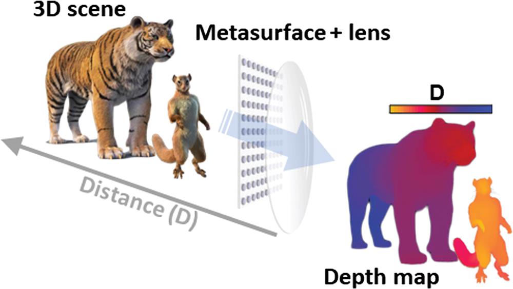
In the current issue of Advanced Photonics, Jin et al.11 present a novel approach to realize 3D imaging by combining a metasurface-based phase mask, which generates a double-helix point spread function (DH-PSF), and a conventional lens for imaging. Through this approach, light from a point source illuminates the designed phase mask, which is implemented by a silicon Huygens metasurface, to realize a DH-PSF. Finally, the image is formed by a lens. The DH-PSF consists of two foci that will rotate around a central point when the distance between the point source and the lens is changed, providing a novel approach to retrieve the depth information of a 3D object scene.12 This effect can be used to obtain wide-field 3D-imaging of a volume object or nonplanar surface (Fig. 1). The approach requires only one camera and doesn’t need any specific light illumination. Using a silicon metasurface enables high transmission efficiency (above 96%) and precise control of spectral and polarization degrees of freedom. It is worth noting that, via exploiting the metal-oxide-semiconductor compatibility, silicon-based metasurfaces offer the unique possibility of integration with other nanophotonic structures and linking to existing integrated photonic architectures.
Sign up for Advanced Photonics TOC. Get the latest issue of Advanced Photonics delivered right to you!Sign up now

Figure 1.Schematic of the depth perception of a 3D object scene with a metasurface.
The innovative idea proposed and experimentally demonstrated by Jin et al.11 could serve as a new paradigm not only for reproducing the functions of bulk optics with nanostructures, but also for manipulating light in ways that are not otherwise feasible with conventional optical components. With this new development, it is feasible to implement an additional metasurface “lens” directly in the metasurface phase mask, leading to a single ultra-thin optical element for 3D imaging. This will help to reduce the size, weight, and cost of future high-performance 3D imaging systems, enabling ultra-compactness, easy integration, and design flexibility for various applications, such as super-resolution imaging, biomedical imaging, particle tracking, robotic vision, and many others.
References
[1] P. Lalanne et al. Blazed binary subwavelength gratings with efficiencies larger than those of conventional échelette gratings. Opt. Lett., 23, 1081-1083(1998).
[2] Z. Bomzonet et al. Pancharatnam-Berry phase in space-variant polarization-state manipulations with subwavelength gratings. Opt. Lett., 26, 1424-1426(2001).
[3] N. Yu et al. Light propagation with phase discontinuities: generalized laws of reflection and refraction. Science, 334, 333-337(2011).
[4] N. I. Zheludev, Y. S. Kivshar. From metamaterials to metadevices. Nat. Mater., 11, 917-924(2012).
[5] M. Khorasaninejad, F. Capasso. Metalenses: versatile multifunctional photonic components. Science, 358, eaam8100(2017).
[6] D. N. Neshev, I. Aharonovich. Optical metasurfaces: new generation building blocks for multi-functional optics. Light: Sci. App., 7, 58(2018).
[7] O. H. Karatas, E. Toy. Three-dimensional imaging techniques: a literature review. Eur. J. Dent., 8, 132-140(2014).
[8] J. Geng. Structured-light 3D surface imaging: a tutorial. Adv. Opt. Photonics, 3, 128-160(2011).
[9] Z. Yang et al. Generalized Hartmann-Shack array of dielectric metalens sub-arrays for polarimetric beam profiling. Nat. Commun., 9, 4607(2018).
[10] R. J. Lin et al. Achromatic metalens array for full-colour light-field imaging. Nat. Nanotechnol., 14, 227-231(2019).
[11] C. Jin et al. Dielectric metasurfaces for distance measurements and three-dimensional imaging. Adv. Photonics, 1, 036001(2019).
[12] S. Quirin, R. Piestun. Depth estimation and image recovery using broadband, incoherent illumination with engineered point spread functions. Appl. Opt., 52, A367-A376(2013).