
Alexander Bespaly, Indranuj Dey, Jenya Papeer, Assaf Shaham, Pavel Komm, Ibrahim Hadad, Gilad Marcus, Arie Zigler. Control of amorphous solid water target morphology induced by deposition on a charged surface[J]. High Power Laser Science and Engineering, 2021, 9(3): 03000e37
- High Power Laser Science and Engineering
- Vol. 9, Issue 3, 03000e37 (2021)
Abstract
1 Introduction
Interaction of high-intensity laser pulses with matter is attractive owing to the wide field of applications, such as secondary light sources, X-ray or gamma generation[1,2], electron[3], and ion[4,5] acceleration. Over the years different schemes for laser-based electron and ion acceleration were proposed, such as laser-wakefield acceleration (LWFA)[6], target normal sheath acceleration (TNSA)[7], radiation pressure acceleration (RPA)[8], and collisionless shock acceleration[9]. Improving laser–matter coupling in each of these mechanisms requires specific and delicate target design, such as specially designed gas jets, mass-limited and nanostructured solid targets[10–12]. A particularly promising ion acceleration scheme is one whereby a high-intensity laser interacts with a structured dynamic plasma target[13]. In this mechanism the laser pulse interacts with microstructured ice targets, sometimes plainly referred to as “snow,” deposited on a sapphire substrate[14]. Such an interaction is assumed to benefit from the localized enhancement of the laser electrical field intensity near the tip of the microstructured whisker. Snow targets have shown an enhancement in proton energy using a moderate-power laser system[15]. These targets are ideal structures for proton acceleration because they are rich in hydrogen and can be generated within the experimental chamber during the experiment. In addition, the residual parasitic debris left after the interaction of the laser with such snow targets is water vapor that does contaminate and damage the laser optics. Snow targets were later improved by deposition of snow on the substrate with pre-fabricated nucleation centers and by controlling the aspect ratio of the snow pillars ranging from 1.4 to 3, by varying the flow rate of the water vapor during the deposition[14]. Nevertheless, the size of individual ice pillar structures, in that case, greatly exceeds the focal spot size of the laser (~10 μm2).
In this paper, we present a unique ice target generation technique, obtained by the deposition of water vapor on an electrically charged substrate. The deposition was conducted under conditions suitable for formation of amorphous solid water (ASW) phase. ASW is the most abundant polymorph of H2O, has been observed on interstellar dust, in dense molecular clouds, and comets, and has also been found on planet satellites; it is thereby a focus of interest in astrophysical research aimed at understanding formation processes of objects in solar systems[16,17]. The morphology of this ice-form is described as a needle-like solid having large surface area and various levels of porosity, which was shown to depend on deposition temperatures[18]. Vapor deposited ice appears in amorphous form below 135 K, with transition from low-density ASW (LDA) to high-density ASW (HDA) below 77 K[19,20]. During the observation of ASW deposition in a scanning electron microscope (SEM) vacuum chamber a new morphology was detected. The ASW pillars obtained were organized and aligned along common axis (in contrast to randomly directed), separated from each other and having larger aspect ratio than those reported previously[14]. The uncommon ASW growth patterns were characteristic of the charged regions of the sapphire substrate, induced by the electrical charging of the sapphire substrate, induced by the electron beam of the SEM before the water vapor deposition on the cooled surface.
In this work we report the study of controlled deposition of ASW layers on an electrically charged surface, by altering the electrical charge deposited on the substrate and exposure of the charged and cooled substrate to varying water vapor pressure. The proposed target design provides higher aspect ratio and controlled and organized growth of snow spikes that are suitable for enhanced ion acceleration by laser.
Sign up for High Power Laser Science and Engineering TOC. Get the latest issue of High Power Laser Science and Engineering delivered right to you!Sign up now
2 Experimental setup
The deposition and high-resolution imaging study of ASW morphology was conducted in analytical Quanta 200 environmental scanning electron microscope (ESEM). The schematic is shown in Figure 1. Low-vacuum and high-vacuum modes allowed manipulation of pressure in the ESEM vacuum chamber from 5×10⁻⁶ to 20 Torr, via introduction of various types of gases, including water vapor. The ESEM is equipped with a Gatan C1001 cold stage, designed for imaging of cryogenic samples as well as deposition of ice from water vapor, through a range of temperatures reaching down to 95 K.
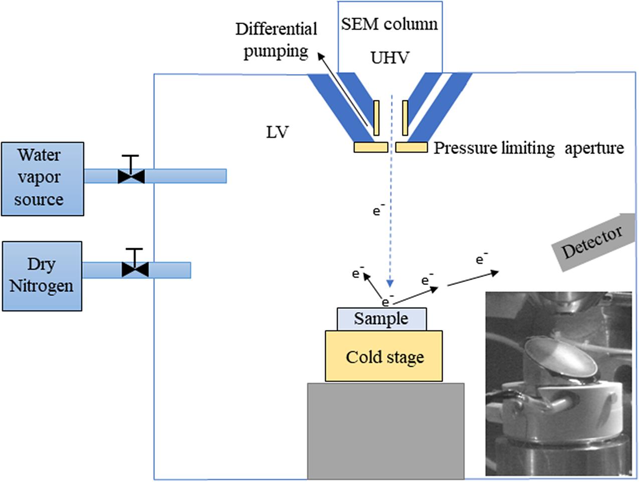
Figure 1.Schematic layout of the experimental system. Water vapor deposits on the cold sample surface under vacuum (LV), and the electron beam responsible both for charging and imaging the deposited layer is injected from an SEM column at ultra-high vacuum (UHV). The secondary electrons detector is also shown. Inset shows an image of deposited ASW layer in ESEM vacuum chamber.
The ASW deposition was studied under varied water vapor pressure, controlled within the 0.3–1.9 Torr range, by a flow metering needle valve. The water vapor nozzle was positioned away from the substrate, and thus the ASW growth process on the substrate is affected only by the ambient pressure in the chamber; the effects of uneven vapor flow are avoided. To estimate the amount of charge accumulated on the substrate before the exposure to the water vapor, the electron current reaching the sample was calibrated using a Faraday cup built in the ESEM sample holder. Current values were varied between 0.44 and 1.57 nA by changing the aperture and the acceleration voltage of the electron gun.
Polished sapphire window, adhered to a custom-made copper holder by a vacuum compatible thermal grease, was used as a substrate for the ice deposition. Initially the substrate was cooled down to 100–115 K, in high vacuum (10-6 Torr). After reaching desired target deposition temperature, the substrate was charged by scanning the target area with a focused electron beam (e-beam). Charging was performed both on a bare sapphire and on a thin buffer layer of pre deposited ASW. Under the experimental conditions there was no thermal degradation of ASW buffer layer owing to exposure to the e-beam. The charged substrate was then exposed to water vapors, in a low-vacuum mode of ESEM. The ASW growth was quenched by replacing water vapor with N2 gas. The obtained ice morphology was imaged in the low-vacuum mode under 0.3 Torr N2 pressure, because ASW is subject to charging.
3 Results
The preliminary study of ASW deposition on a charged surface was performed on a bare sapphire substrate. After charging an area of 500 μm× 500 μm for 300 s at 0.44 nA, the sapphire was exposed to water vapor at 1.2 Torr for 60 s. The resulting ice layer is shown in Figure 2(a), with clearly visible topology variation present in the layer. The area affected by charging is about two orders of magnitude larger than the area irradiated with electrons. The increased dimensions of the charged area can be attributed to charge diffusion caused by a lack of surface defects on the polished sapphire, and an e-beam deflection owing to charge build up[21].
![]()
Figure 2.SEM image of ASW layer deposited at 1.2 Torr vapor pressure, on charged sapphire surface: (a) complete area affected by surface charge; (b) high-magnification image of ASW, with the left-hand side of the image showing cauliflower-like shaped grains affected by the surface charge and the right-hand side showing the dense and flat ASW.
The ASW morphology varies at different regions of the obtained layer. Figure 2(b) shows two different types of morphologies: flat and dense in the valleys (dark regions in Figure 2(a)), comparable with usual ASW morphology grown at same deposition rates[22], and less dense cauliflower-like morphology, obtained on the hill (brighter region in Figure 2(a)). This points towards different deposition kinetics affected by surface charge. A similar deposition variation can be observed when the deposition is conducted on artificial nucleation centers and on an unnucleated adjacent area[14].
To reduce the surface diffusion of the electrons, the flat ASW buffer layer was chosen as a substrate for charging. Figure 3(a) shows typical morphology of ASW layer grown at 1.2 Torr water vapor pressure with the substrate at 105 K. The bright lines on the grain boundaries represent initiation of charging under operation at high-vacuum mode of ESEM. Subsequent deposition of water vapor on such a buffer layer of ASW with an accumulated charge resulted in a morphological change of the next ASW layer (Figures 3(b)–3(d)). The morphological change appeared only in the area confined by e-beam scan, resulting in elongated ASW pillars. The area covered by the pillars is slightly larger than the area scanned initially by the e-beam, in contrast to deposition on a charged sapphire.
![]()
Figure 3.(a) ASW deposited on sapphire substrate before charging; (b) ASW target deposited at 1.9 Torr, after 60 s charging; (c) ASW target deposited at 1.5 Torr, after 60 s charging; and (d) ASW target deposited at 1.5 Torr, after 120 s charging.
The charging of the substrate surface under e-beam raster scanning is a complex phenomenon. However, it can be assumed that the electric field is generated on the surface, in a manner similar to a plane capacitor[23,24]. The generated electric field polarizes the orientation of the water dipoles, leading to induced deposition along the electric field lines[25]. This can point towards formation of elongated ASW pillars deposited on a charged surface.
Structures shown in Figures 3(c) and 3(d) were deposited on a buffer layer of ASW having different charging times of 60 s and 120 s, respectively, at 1.5 Torr pressure and a temperature of 103 K. The current of the e-beam was 1.57 nA, and the scanned area was 100 μm × 100 μm. The effect of the charge amount on a layer morphology is clearly visible from these two images, longer exposure time of the e-beam leading to increased aspect ratio of individual pillars, without much influence on the cauliflower morphology. Figure 3(b) shows an image of ASW deposited at similar charging conditions as in case Figure 3(c), but for a scanned area of 200 μm × 200 μm and grown under exposure to 1.9 Torr, at 104 K. For the deposition case shown in Figure 3(b), it can be noted that the highest pillars formed on the periphery of the scanned area. The morphology of these pillars varies from those obtained under exposure to 1.5 Torr (Figures 3(c) and 3(d)), having anisotropic domains elongated parallel to the pillar direction.
The pillar dimensions were analyzed using high-magnification ESEM images of ASW targets deposited at different conditions. For each deposition case, the height and diameter of approximately 10–15 randomly chosen pillars were measured. The pillar height is defined from the surface of the layer to the tip, and the diameter was measured near the pillar tip. The average measurements and standard deviation are summarized in Table 1. Longer charging time led to the formation of higher pillars with relatively small diameter having an average aspect ratio of 5.1. Targets grown under exposure to 1.9 Torr of water vapor showed a slightly increased aspect ratio of 2.6 compared with those grown at 1.5 Torr having an aspect ratio of 1.7, having same charging conditions.
| Charging | Vapor | Average | Average | Average |
|---|---|---|---|---|
| time | pressure | height | diameter | aspect |
| (s) | (Torr) | (μm) | (μm) | ratio |
| 60 | 1.5 | 21.3±4.2 | 12.8±2.5 | 1.7 |
| 120 | 1.5 | 45.1±14.3 | 9.5±2.9 | 5.1 |
| 60 | 1.9 | 22.7±3.5 | 9.3±2.5 | 2.6 |
Table 1. Effect of deposition condition on ASW target morphology.
Figures 4(a)–4(c) show the high-magnification images of the three ASW targets described previously. Structures obtained after deposition at 1.5 Torr (Figures 4(a) and 4(b)) consist of small spherical grains with an average diameter of 2.5±0.5 μm, and the difference between the two targets (Figures 4(a) and 4(b)) was observed only in the aspect ratio of pillars, owing to different charging time. There is a significant difference in the internal structure of ASW target deposited at 1.9 Torr, which can be seen in Figure 4(c). The internal microstructure appears to be anisotropic, having whisker-like elongated grains oriented parallel to the pillar axis. The grains have an average diameter of 1.3±0.2 μm. As was shown earlier[14], the deposition rate has a significant role in single pillar morphology, and thus the aspect ratio of this structure is higher than of those deposited at 1.5 Torr with the same charging conditions.
![]()
Figure 4.(a) ASW target deposited at 1.5 Torr, after 60 s charging; (b) ASW target deposited at 1.5 Torr, after 120 s charging; (c) ASW target deposited at 1.9 Torr, after 60 s charging.
The deposition of charged ASW was not observed in all experiments. It was found that experiments conducted at temperatures above 110 K resulted in flat ASW films, similar to the deposition without accumulated charge on the buffer layer (Figure 3(a)). Sagi et al.[26] have shown that at temperatures above 110 K the increased thermal energy of ASW layer allows a faster mobility of electrons in ASW buffer layer, which results in a deeper penetration of the electrons. This process leads to solvation of electrons in ASW matrices resulting in a reduced electric field on the ASW surface.
During deposition under exposure to a vapor pressure bellow 0.8 Torr, after charging the substrate for 60 s at 1.57 nA, the ASW layer appeared with distorted shape or having low aspect ratio. At low vapor pressures the water molecules neutralize the surface charge before being attached. This is a known mechanism of a charge neutralization in low-vacuum SEMs[27]. The ASW layer shown in Figure 5 was deposited at 0.7 Torr vapor pressure. The obtained charged fraction of the ASW layer consists mainly of small cauliflower-shaped domains, present on the edges of the scanned frame. Owing to such behavior of water molecules, the charged ASW targets can only be obtained by deposition on a substrate having temperature below 110 K, with the exposure to water vapor pressure above 0.8 Torr.
![]()
Figure 5.ASW deposited at 0.7 Torr, on a buffer ASW layer after 60 s charging at 1.57 nA.
4 Summary
Deposition of water vapor on a charged ASW surface showed a variety of growth kinetics, resulting in well-separated features and increased aspect ratio. ASW targets can be deposited with a wide range of aspect ratio of pillars from 1.7 to 5.1 and varying grain morphology, averaged over four to five depositions under the same experimental conditions. The ASW target morphology is highly dependent on charging conditions, water vapor pressure, and temperature. It was also shown that the suitable conditions for the charged ASW target deposition are substrate temperatures below 110 K and vapor pressure above 0.8 Torr.
The fact that structures can be redeposited within several minutes without breaking vacuum, and their feature diameter comparable with the spot size of the laser focus in a typical laser–plasma interaction experiment, make them attractive as potential targets for today’s high-repetition-rate laser systems.
References
[1] E. N. Nerush, I. Y. Kostyukov, L. Ji, A. Pukhov. Phys. Plasmas, 21, 013109(2014).
[2] L. T. Hudson, J. F. Seely. Radiat. Phys. Chem., 79, 132(2010).
[3] M. Galletti, F. G. Bisesto, M. P. Anania, M. Ferrario, R. Pompili, A. Poyé, A. Zigler. Opt. Lett., 45, 4420(2020).
[4] H. Schwoerer, S. Pfotenhauer, O. Jäckel, K.-U. Amthor, B. Liesfeld, W. Ziegler, R. Sauerbrey, K. W. D. Ledingham, T. Esirkepov. Nature, 439, 445(2006).
[5] M. Bailly-Grandvaux, D. Kawahito, C. McGuffey, J. Strehlow, B. Edghill, M. S. Wei, N. Alexander, A. Haid, C. Brabetz, V. Bagnoud, R. Hollinger, M. G. Capeluto, J. J. Rocca, F. N. Beg. Phys. Rev. E, 102, 021201(2020).
[6] J. Osterhoff, A. Popp, Z. Major, B. Marx, T. P. Rowlands-Rees, M. Fuchs, M. Geissler, R. Hörlein, B. Hidding, S. Becker, E. A. Peralta, U. Schramm, F. Grüner, D. Habs, F. Krausz, S. M. Hooker, S. Karsch. Phys. Rev. Lett., 101, 085002(2008).
[7] S. C. Wilks, A. B. Langdon, T. E. Cowan, M. Roth, M. Singh, S. Hatchett, M. H. Key, D. Pennington, A. MacKinnon, R. A. Snavely. Phys. Plasmas, 8, 542(2001).
[8] S. V. Bulanov, E. Yu. Echkina, T. Zh. Esirkepov, I. N. Inovenkov, M. Kando, F. Pegoraro, G. Korn. Phys. Rev. Lett., 104, 135003(2010).
[9] F. Fiuza, A. Stockem, E. Boella, R. A. Fonseca, L. O. Silva, D. Haberberger, S. Tochitsky, W. B. Mori, C. Joshi. Phys. Plasmas, 20, 056304(2013).
[10] J. L. Henares, P. Puyuelo-Valdes, F. Hannachi, T. Ceccotti, M. Ehret, F. Gobet, L. Lancia, J.-R. Marquès, J. J. Santos, M. Versteegen, M. Tarisien. Rev. Sci. Instrum, 90, 063302(2019).
[11] I. Prencipe, A. Sgattoni, D. Dellasega, L. Fedeli, L. Cialfi, W. Choi, I. J. Kim, K. A. Janulewicz, K. F. Kakolee, H. W. Lee. Plasma Phys. Control. Fusion, 58, 034019(2016).
[12] T. Ebert, N. W. Neumann, T. Abel, G. Schaumann, M. Roth. High Power Laser Sci. Eng., 5(2017).
[13] A. Zigler, S. Eisenman, M. Botton, E. Nahum, E. Schleifer, A. Bespaly, I. Pomerantz, F. Abicht, J. Branzel, G. Priebe, S. Steinke, A. Andreev, M. Schnuerer, W. Sandner, D. Gordon, P. Sprangle, K. W. D. Ledingham. Phys. Rev. Lett, 110, 215004(2013).
[14] E. Schleifer, E. Nahum, M. Botton, Z. Henis, A. Zigler. J. Phys. D, 48, 085502(2015).
[15] A. Zigler, T. Palchan, N. Bruner, E. Schleifer, S. Eisenmann, M. Botton, Z. Henis, S. A. Pikuz, A. Y. Faenov, D. Gordon, P. Sprangle. Phys. Rev. Lett, 106, 134801(2011).
[16] R. Smoluchowski. Science, 201, 809(1978).
[17] R. Yokochi, U. Marboeuf, E. Quirico, B. Schmitt. Icarus, 218, 760(2012).
[18] A. Bar-Nun, I. Kleinfeld, E. Kochavi. Phys. Rev. B, 38, 7749(1988).
[19] T. Loerting, W. Schustereder, K. Winkel, C. G. Salzmann, I. Kohl, E. Mayer. Phys. Rev. Lett., 96(2006).
[20] G. A. Kimmel, K. P. Stevenson, Z. Dohnálek, R. S. Smith, B. D. Kay. J. Chem. Phys., 114, 5284(2001).
[21] S. Fakhfakh, O. Jbara, M. Belhaj, Z. Fakhfakh, A. Kallel, E. I. Rau. Nucl. Instrum. Methods Phys. Res. B, 197, 114(2002).
[22] J. H. E. Cartwright, B. Escribano, C. I. Sainz-Díaz. Thin Solid Films, 518, 3422(2010).
[23] K. Kanaya, N. Ichise, K. Adachi, K. Yonehara, Y. Muranaka. Micron Microsc. Acta, 23, 319(1992).
[24] J. Cazaux. J. Microsc., 217, 16(2005).
[25] X. Zhu, Q. Yuan, Y. P. Zhao. Nanoscale, 6, 5432(2014).
[26] R. Sagi, M. Akerman, S. Ramakrishnan, M. Asscher. J. Phys. Chem. C, 122, 9985(2018).
[27] R. F. Egerton. Physical Principles of Electron Microscopy(2016).

Set citation alerts for the article
Please enter your email address
© Copyright 2018-2021 | Chinese Laser Press. All Rights Reserved 沪ICP备15018463号-20