• Advanced Photonics
  • Vol. 3, Issue 2, 024002 (2021)
Dezhi Tan1、*, Zhuo Wang1, Beibei Xu1, and Jianrong Qiu1、2、*
Author Affiliations
  • 1Zhejiang University, College of Optical Science and Engineering, State Key Laboratory of Modern Optical Instrumentation, Hangzhou, China
  • 2Chinese Academy of Sciences, CAS Center for Excellence in Ultra-Intense Laser Science, Shanghai, China
  • show less
    DOI: 10.1117/1.AP.3.2.024002 Cite this Article Set citation alerts
    Dezhi Tan, Zhuo Wang, Beibei Xu, Jianrong Qiu. Photonic circuits written by femtosecond laser in glass: improved fabrication and recent progress in photonic devices[J]. Advanced Photonics, 2021, 3(2): 024002 Copy Citation Text show less
    WGs written by fs lasers in glass: improved fabrication techniques and photonic device applications.
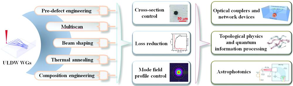
    Fig. 1. WGs written by fs lasers in glass: improved fabrication techniques and photonic device applications.
    Beam evolution near focus (a) without and (d) with a slit, energy distribution in the YZ plane (b) without and (e) with a slit, optical images of fabricated WGs in phosphate glass (c) without and (d) with a slit (Wy=500 μm). X corresponds to the fs laser beam translation direction. Figures reproduced from Ref. 25. (g) Aspect ratio of the WGs produced in the fused silica with a slit Wy of 350 μm. Dotted line: aspect ratio of 1. (h) Propagation loss at 1550 nm as a function of depth (Wy=250 μm). Figures reproduced from Ref. 26.
    Fig. 2. Beam evolution near focus (a) without and (d) with a slit, energy distribution in the YZ plane (b) without and (e) with a slit, optical images of fabricated WGs in phosphate glass (c) without and (d) with a slit (Wy=500  μm). X corresponds to the fs laser beam translation direction. Figures reproduced from Ref. 25. (g) Aspect ratio of the WGs produced in the fused silica with a slit Wy of 350  μm. Dotted line: aspect ratio of 1. (h) Propagation loss at 1550 nm as a function of depth (Wy=250  μm). Figures reproduced from Ref. 26.
    (a) Schematic of the WG writing setup with astigmatic beam shaping. Figure reproduced from Ref. 31. Simulated electron density profiles (b) without and with astigmatic beam shaping for different focusing parameters (c) w0x=1 μm, w0y=3 μm, z0=0, (d) w0x=1 μm, w0y=3 μm, z0=100 μm, and (e) w0x=1.4 μm, w0y=4.2 μm, z0=260 μm. Figures reproduced from Ref. 29.
    Fig. 3. (a) Schematic of the WG writing setup with astigmatic beam shaping. Figure reproduced from Ref. 31. Simulated electron density profiles (b) without and with astigmatic beam shaping for different focusing parameters (c) w0x=1  μm, w0y=3  μm, z0=0, (d) w0x=1  μm, w0y=3  μm, z0=100  μm, and (e) w0x=1.4  μm, w0y=4.2  μm, z0=260  μm. Figures reproduced from Ref. 29.
    (a) Schematic illustration of fs laser SSTF. Calculated laser intensity distributions at the focus generated by an objective lens (b) without and (c), (d) with the SSTF technique in the XZ and YZ planes, respectively. Figures reproduced from Ref. 30. (e) Schematic of the experimental setup for adding an initial temporal chirp on the SSTF. AP, aperture; VF, variable neutral density filter; GR1 and GR2, gratings; OBJ, objective lens; SA, sample. (f) Cross-sectional view optical micrographs of the line written at 9 mm. Scale bar, 20 μm. Figures reproduced from Ref. 50.
    Fig. 4. (a) Schematic illustration of fs laser SSTF. Calculated laser intensity distributions at the focus generated by an objective lens (b) without and (c), (d) with the SSTF technique in the XZ and YZ planes, respectively. Figures reproduced from Ref. 30. (e) Schematic of the experimental setup for adding an initial temporal chirp on the SSTF. AP, aperture; VF, variable neutral density filter; GR1 and GR2, gratings; OBJ, objective lens; SA, sample. (f) Cross-sectional view optical micrographs of the line written at 9 mm. Scale bar, 20  μm. Figures reproduced from Ref. 50.
    (a) Schematic of the focusing geometry. (b) Simulated estimate of the focal peak intensity Ip at various depths in glass. (c) Δz as a function of depth. WGs inscribed at different depths (d) without and (e) with aberration correction in the nonthermal writing regime (pulse repetition rate of 1 kHz). Figures reproduced from Ref. 59. (f) Plot of the transmission throughput and mode ellipticity as a function of depth for WGs inscribed with SLM beam shaping at the thermal writing regime (pulse repetition rate of 1 MHz). Figure reproduced from Ref. 24.
    Fig. 5. (a) Schematic of the focusing geometry. (b) Simulated estimate of the focal peak intensity Ip at various depths in glass. (c) Δz as a function of depth. WGs inscribed at different depths (d) without and (e) with aberration correction in the nonthermal writing regime (pulse repetition rate of 1 kHz). Figures reproduced from Ref. 59. (f) Plot of the transmission throughput and mode ellipticity as a function of depth for WGs inscribed with SLM beam shaping at the thermal writing regime (pulse repetition rate of 1 MHz). Figure reproduced from Ref. 24.
    (a) Cross-sections of WGs written by scanning fs lasers 1, 2, 4, 6, and 10 times. (b) Schematic view of temperature gradient assistant fs laser writing. Black arrow: matter expansion and flow driven by temperature gradient and stress. White arrows: stress. (c) Insertion loss and diameter (w) of WGs fabricated by scanning various times at 300 μm. Inset: I, cross-section; II, near-field mode profile. Figure reproduced from Ref. 67. (d) Left: illustration of the dependency of the WG cross-section on the fs laser power. Right: cross section of WGs tapered by multiscanning with a low power at the end of the WG. Figures reproduced from Ref. 68. (f) Schematic of the multiscan WG fabrication with an offset perpendicular to the writing direction. Figure reproduced from Ref. 69. (g) Size variation with an increase in the number of scans. Figure reproduced from Ref. 70. (h) Schematic of the sandwiched WG. Insets: the cross sections of the WG and bend-loss-suppression walls. Scale bar: 30 μm. (i) Top view of the sandwiched WG. (j) A 633-nm laser beam propagating in the WG. Top view images of a WG bend (k) without and (l) with bend-loss-suppression walls. Figures reproduced from Ref. 71.
    Fig. 6. (a) Cross-sections of WGs written by scanning fs lasers 1, 2, 4, 6, and 10 times. (b) Schematic view of temperature gradient assistant fs laser writing. Black arrow: matter expansion and flow driven by temperature gradient and stress. White arrows: stress. (c) Insertion loss and diameter (w) of WGs fabricated by scanning various times at 300  μm. Inset: I, cross-section; II, near-field mode profile. Figure reproduced from Ref. 67. (d) Left: illustration of the dependency of the WG cross-section on the fs laser power. Right: cross section of WGs tapered by multiscanning with a low power at the end of the WG. Figures reproduced from Ref. 68. (f) Schematic of the multiscan WG fabrication with an offset perpendicular to the writing direction. Figure reproduced from Ref. 69. (g) Size variation with an increase in the number of scans. Figure reproduced from Ref. 70. (h) Schematic of the sandwiched WG. Insets: the cross sections of the WG and bend-loss-suppression walls. Scale bar: 30  μm. (i) Top view of the sandwiched WG. (j) A 633-nm laser beam propagating in the WG. Top view images of a WG bend (k) without and (l) with bend-loss-suppression walls. Figures reproduced from Ref. 71.
    Cross sections of the WGs (a) before and (b) after thermal annealing. Refractive index profiles of WG (c) before and (d) after annealing. (e) Normalized output through the WGs as a function of bend radii. Figures reproduced from Ref. 86. (f) PL intensity versus depth in the glass after X-ray exposure with various doses. (g) Change of refractive index (Δn) in the WGs as a function of the scan speed at different X-rays doses. Figures reproduced from Ref. 34.
    Fig. 7. Cross sections of the WGs (a) before and (b) after thermal annealing. Refractive index profiles of WG (c) before and (d) after annealing. (e) Normalized output through the WGs as a function of bend radii. Figures reproduced from Ref. 86. (f) PL intensity versus depth in the glass after X-ray exposure with various doses. (g) Change of refractive index (Δn) in the WGs as a function of the scan speed at different X-rays doses. Figures reproduced from Ref. 34.
    (a) Illustration of the double-track approach for fabrication of WGs and RPDCs. θ is the geometrically radial and azimuthal offset between two adjacent tracks (dark red) in each WG (gray). (b) Polarization analysis of the 45-deg rotated parallel coupling region with different linear input states [H, V, antidiagonal (135 deg, A Pol.) and diagonal (45 deg, D Pol.)]. Figures reproduced from Ref. 43. (c) Schematic of a DC. Two input (out) ports: IN1 and IN2 (OUT1 and OUT2). (d) Transmission and reflection extinction ratios for a PDC with L of 33.2 mm and d of 12.5 μm in the telecom band. (e) Transmission for polarization insensitive DCs with L of 0.4 to 1.3 mm and d of 8 μm. Figures reproduced from Ref. 111. (f) Diagram of the 4-core few-mode coupler. Figure reproduced from Ref. 114. (g) Schematic of the optical add-drop multiplexer configuration. Figure reproduced from Ref. 115.
    Fig. 8. (a) Illustration of the double-track approach for fabrication of WGs and RPDCs. θ is the geometrically radial and azimuthal offset between two adjacent tracks (dark red) in each WG (gray). (b) Polarization analysis of the 45-deg rotated parallel coupling region with different linear input states [H, V, antidiagonal (135 deg, A Pol.) and diagonal (45 deg, D Pol.)]. Figures reproduced from Ref. 43. (c) Schematic of a DC. Two input (out) ports: IN1 and IN2 (OUT1 and OUT2). (d) Transmission and reflection extinction ratios for a PDC with L of 33.2 mm and d of 12.5  μm in the telecom band. (e) Transmission for polarization insensitive DCs with L of 0.4 to 1.3 mm and d of 8  μm. Figures reproduced from Ref. 111. (f) Diagram of the 4-core few-mode coupler. Figure reproduced from Ref. 114. (g) Schematic of the optical add-drop multiplexer configuration. Figure reproduced from Ref. 115.
    (a) Schematic for an 84-channel interposer in glass, fanning out from a linear array (silica photonic chip at back) to 12 socket positions for multicore fibers (MCFs) packaging. (b) Optical image of the interposer in silica glass. Figures reproduced from Ref. 120.
    Fig. 9. (a) Schematic for an 84-channel interposer in glass, fanning out from a linear array (silica photonic chip at back) to 12 socket positions for multicore fibers (MCFs) packaging. (b) Optical image of the interposer in silica glass. Figures reproduced from Ref. 120.
    (a) Sketch of the helical WGs with honeycomb geometry. (b) Optical image of the input facet of the photonic lattice. Figures reproduced from Ref. 127. Schematic diagram of honeycomb lattices with (c) armchair and (d) zigzag edge domain walls. Red and green WGs exhibit a different refractive index, and blue is the excitation WGs. Red-shaded regions are domain walls. Figures reproduced from Ref. 132.
    Fig. 10. (a) Sketch of the helical WGs with honeycomb geometry. (b) Optical image of the input facet of the photonic lattice. Figures reproduced from Ref. 127. Schematic diagram of honeycomb lattices with (c) armchair and (d) zigzag edge domain walls. Red and green WGs exhibit a different refractive index, and blue is the excitation WGs. Red-shaded regions are domain walls. Figures reproduced from Ref. 132.
    (a) Topological bandgap for the Floquet topological insulator in a helical honeycomb lattice. (b) Breaking the parity structure symmetry by detuning the sublattices with formation of a trivial bandgap. (c) Forming topological Anderson insulator phase by suppressing the effect of the parity-symmetry breaking terms with sufficiently strong disorder. (d) Hybrid structure with a 1D straw and a 2D honeycomb helical WG lattice. The excited state was controlled by the “straw”—through which the modes of the system were selectively excited. Excitation light along the edge states in the (e) Floquet topological insulator, (f) trivial insulator, and (g) topological Anderson insulator. The input positions were indicated by the white arrows. Figures reproduced from Ref. 137.
    Fig. 11. (a) Topological bandgap for the Floquet topological insulator in a helical honeycomb lattice. (b) Breaking the parity structure symmetry by detuning the sublattices with formation of a trivial bandgap. (c) Forming topological Anderson insulator phase by suppressing the effect of the parity-symmetry breaking terms with sufficiently strong disorder. (d) Hybrid structure with a 1D straw and a 2D honeycomb helical WG lattice. The excited state was controlled by the “straw”—through which the modes of the system were selectively excited. Excitation light along the edge states in the (e) Floquet topological insulator, (f) trivial insulator, and (g) topological Anderson insulator. The input positions were indicated by the white arrows. Figures reproduced from Ref. 137.
    (a) Triangular photonic lattices with a defect in a straight WG array. (b) Observation of the “fractionalized” corner states. Red circle: injection of 720-nm coherent light into the WG at the corner indicated. Green circle: missing WGs. Figures reproduced from Ref. 140.
    Fig. 12. (a) Triangular photonic lattices with a defect in a straight WG array. (b) Observation of the “fractionalized” corner states. Red circle: injection of 720-nm coherent light into the WG at the corner indicated. Green circle: missing WGs. Figures reproduced from Ref. 140.
    Schematic diagrams of (a) a photonic-chip-based glued binary tree, (b) the proposed hexagonal WG photonic chips, and (c) the quantum fast hitting experiment on the WG photonic chips. (d) Optimal hitting efficiency for hexagonal photonic chips at different layer depths. Figure reproduced from Ref. 149. (e) The estimated computing time for the photonic computer and other competitors. Figure reproduced from Ref. 150.
    Fig. 13. Schematic diagrams of (a) a photonic-chip-based glued binary tree, (b) the proposed hexagonal WG photonic chips, and (c) the quantum fast hitting experiment on the WG photonic chips. (d) Optimal hitting efficiency for hexagonal photonic chips at different layer depths. Figure reproduced from Ref. 149. (e) The estimated computing time for the photonic computer and other competitors. Figure reproduced from Ref. 150.
    (a) Schematic of a photonic dicer consisting of the 3D WG lattices combining photonic lantern and reformatting functions. I: multicode input end with 6×6 array WGs in 2D; II: pseudoslit output end with 36 array WGs in 1D. Figures reproduced from Ref. 159. (b) Schematic of an on-chip two-port nulling interferometer chip in GLS glass. Figure reproduced from Ref. 162. (c) The photonic assembly includes the nulling chip, the microlens array (MLA), and fiber V-groove. (d) The WG arrangement in the photonic chip. Figure reproduced from Ref. 80.
    Fig. 14. (a) Schematic of a photonic dicer consisting of the 3D WG lattices combining photonic lantern and reformatting functions. I: multicode input end with 6×6 array WGs in 2D; II: pseudoslit output end with 36 array WGs in 1D. Figures reproduced from Ref. 159. (b) Schematic of an on-chip two-port nulling interferometer chip in GLS glass. Figure reproduced from Ref. 162. (c) The photonic assembly includes the nulling chip, the microlens array (MLA), and fiber V-groove. (d) The WG arrangement in the photonic chip. Figure reproduced from Ref. 80.
    Dezhi Tan, Zhuo Wang, Beibei Xu, Jianrong Qiu. Photonic circuits written by femtosecond laser in glass: improved fabrication and recent progress in photonic devices[J]. Advanced Photonics, 2021, 3(2): 024002
    Download Citation