
Lingjun Yi, Changhong Li. Enhanced absorption and electrical modulation of graphene based on the parity-time symmetry optical structure[J]. Chinese Optics Letters, 2022, 20(2): 022201
- Chinese Optics Letters
- Vol. 20, Issue 2, 022201 (2022)
Abstract
Keywords
1. Introduction
Graphene is a two-dimensional (2D) atomic scale hexagonal carbon isomorphism. Its conduction band and valence band meet at the Dirac point. Accordingly, graphene is equivalent to a zero-gap semiconductor with electron mobility exceeding at room temperature[
For the general periodic photonic crystal structure, when studying the transmission, reflection, and absorption of light, the gain and loss of the medium are often not considered, or the loss of the medium is regarded as an adverse factor. But, for optical structures that satisfy parity-time (PT) symmetry, quantum dots are anthropogenically introduced into the substrate medium forming gain and loss dielectric layers. When the gain and loss dielectric layers are accurately anastomotic, a bizarre optical transmission phenomenon can be produced under the action of external pump energy[
Based on the special optical properties of the PT symmetry structure, we take the graphene as the top layer, with the photonic crystals satisfying the PT symmetry structure as the bottom layer, so we realized the ultrastrong absorption of graphene. Meanwhile, the modulation of graphene absorption is achieved by using the photoelectric effect of crystals.
Sign up for Chinese Optics Letters TOC. Get the latest issue of Chinese Optics Letters delivered right to you!Sign up now
2. Model Design and Theoretical Calculation
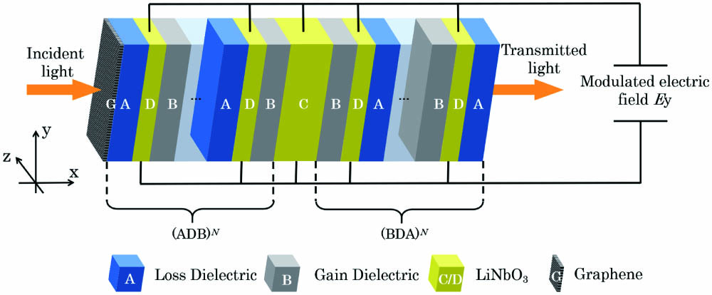
The overall structure is designed as shown schematically in Fig. 1, where each dielectric layer can be simply represented as . Thereinto, the G deputies graphene layer is placed to the forward side of the PT symmetry photonic crystal. For the underlying structure, the gain–loss layers are formed by doping quantum dots in the substrate dielectric silica, denoted by A and B, respectively. Such gain or loss dielectric layers can be realistically manufactured by analogy to quantum well amplifiers or photorefractive structures. We can use a modified solution doping method in the modified chemical vapor deposition (MCVD) process to develop a gain-doped or loss-doped silica substrate[
![]()
Figure 1.Schematic diagram of the proposed structure.
The D and C layers represent crystal, which is a typical optical functional material, and its refractive index will vary with the applied electric field and satisfies the ellipsoid equation. In this paper, the TE wave is selected as the incident wave, and its electric field is distributed along the axis. When the applied electric field direction is along the axis, the refractive index of the D or C layer can be expressed as[
For the graphene layer on the top, the optical properties are closely related to its complex surface conductivity . Its effective dielectric constant can be expressed as[
The transmission matrix method (TMM) is used to study the absorption characteristics of graphene in this paper, and the detailed description of the TMM is shown in relevant literature[
3. Results and Discussion
To satisfy the PT symmetry condition and make the defect mode be generated at 1550 nm, in numerical calculations, the thickness of the A and B layers is set to for the underlying PT symmetry photonic crystal. The macroscopic Lorentz oscillation intensity and . By adjusting the thickness of the D dielectric layer to , the thickness of the C dielectric layer is , as the defect layer of the whole structure. Without the external electric field, the refractive index of the D and C layers is . The chemical potential for monolayer graphene, and the PT symmetry structure period is . Figure 2 shows the transmission and reflection of the whole structure and the absorption spectra of monolayer graphene with the condition of normal incidence. Since there is a large difference in the numerical value, here, logarithmic transformation, with decibels (dB) as the unit, is taken for the transmission during calculation. The transformation relation can be written as , where can represent the transmission and reflection of the whole structure and the absorption of monolayer graphene.
![]()
Figure 2.Transmission and reflection spectra of the whole structure and the absorption spectra of the graphene layer.
As clearly seen in Fig. 2, at the wavelength of 1550 nm, the transmission and reflection of the whole structure can reach 13.71 dB and 11.72 dB, respectively. The absorption of monolayer graphene can reach , which is 17 times of the absorption of monolayer graphene in air. From Eq. (1), it can be seen that only the working light wave is at 1550 nm, and the refractive index of the A and B layers can strictly satisfy the PT symmetry condition when is opted as the central wavelength (the real part of the gain–loss layer is even symmetric, and the imaginary part is odd symmetric). Under such circumstances, the PT symmetry structure has the strongest amplification effect on the transmission and reflection of the incident light, and the graphene–light interactions are tremendously enhanced; this is the dominating cause for the ultrastrong absorption of graphene. As can be seen from Eq. (8) and Fig. 2, both simulation results and theoretical analysis agree very well.
Macroscopic Lorentz oscillation intensity of the underlying PT symmetry photonic crystal, the incident light angle, and the chemical potential are the predominant factors affecting graphene absorption. The following analysis focuses on the influence of macroscopic Lorentz oscillation intensity, the incident light angle, and the chemical potential on graphene absorption.
The value of macroscopic Lorentz oscillation intensity has a prodigiously greater influence on the imaginary part of the gain–loss dielectric layer, and then it affects the resonance coupling effect of the whole structure. In order to demonstrate the effects of on the absorption of graphene, firstly, keeping the other parameters constant, we present the graphene absorption spectrum with different values in Fig. 3(a). The results show that the peak position of graphene absorption, with different values, remains unchanged, while the absorption of graphene changes remarkably. Figure 3(b) presents the graphene absorption for to be changed from to in steps of , where the graphene absorption manifests a tendency to increase first and then decrease. The maximum absorption of monolayer graphene can reach 24.5 dB when , which is five orders of magnitude higher for monolayer graphene absorption than in air; this is because the resonant coupling effect of the structure is the strongest at 1550 nm when . The PT symmetry structure in the bottom layer has the maximum efficiency of converting pump energy into incident light wave electromagnetic energy, and the transmission and reflection of the structure are much higher than one, thus amplifying the absorption efficiency of the top layer of graphene. Notice that there is a small fluctuation in the value of near the peak value, which will also have a great impact on the absorption of graphene. For practical application, it is a challenge to control in this order of magnitude. Accordingly, we select for the following calculation.
![]()
Figure 3.(a) Absorption spectrum of graphene with different α values; (b) variation in the absorption at 1550 nm as a function of α.
The influences of the incident light angle on graphene absorption and the absorption peak position are investigated, and the angle response 2D views of graphene absorption are plotted in Fig. 4. It is clearly seen that the absorption mode, deviating from on-resonance position, has a blue shift, and, simultaneously, the absorption drops from 24.5 dB to 1.3 dB quickly with the increasing incident light angle although the incident angle is changed only 10°.
![]()
Figure 4.Angle responses of graphene absorption.
Table 1 details the absorption peak position and the absorption peak value of graphene with different incident angles. The starting peak position of the absorption shifts from 1550 nm to 1541 nm. Due to such angular susceptibility, care is taken to ensure that the graphene absorption is maximum; thus, the vertical incident light is still selected. The electro-modulation properties of graphene absorption based on the electro-optic effect of crystal are discussed below.
| Incident angle (°) | 0 | 2 | 4 | 6 | 8 | 10 |
|---|---|---|---|---|---|---|
| Wavelength (nm) | 1550 | 1549.5 | 1549 | 1547 | 1544 | 1541 |
| Absorption (dB) | 24.5 | 22.4 | 19.9 | 10.7 | 5.2 | 1.3 |
Table 1. Absorption Peak Position and Peak Value at Different Incident Light Angles
In Figs. 5(a) and 5(b), we give the real and imaginary parts of wavelength-dependent , respectively, with the chemical potential to be changed from 0.3 to 0.6 eV in steps of 0.06 eV. We can find in Fig. 5 that a sharp peak in the real part of and a sudden fall in the imaginary part of have a quick blue shift. It can be known from literature[
![]()
Figure 5.(a) and (b) Real and imaginary parts of the complex permittivity of graphene for different chemical potential μ; (c) the absorption of graphene as a function of the chemical potential μ.
According to the sudden fall (or sharp peak) dot position, with the change of the chemical potential , it is clearly seen in Fig. 5 that when the chemical potential is , the sudden fall (or sharp peak) dot position is at 1550 nm; that is, when the chemical potential exceeds 0.42 eV, the absorption of the 1550 nm light wave by monolayer graphene tends to zero. For the proposed structure, in Fig. 5(c), we calculated the absorption of graphene at different chemical potentials for the investigated wavelength of 1550 nm. Apparently, the absorption of graphene begins to drop gradually when the chemical potential is close to or more than 0.42 eV. Accordingly, when setting the chemical potential parameter, the value should be less than 0.42 eV. According to the calculation results in Fig. 5(c), we take as the final optimization result in this paper. At this time, the absorption of monolayer graphene can reach 31.5 dB, which is much higher than the corresponding graphene absorption ( to 0 dB) in Refs. [9–11].
It can be straightforwardly seen from Eq. (3) that the refractive index of crystal is related to the external electric field intensity, and the change of electric field intensity will lead to the change of the crystal refractive index, so the position of the absorption peak will produce a red shift or blue shift. Accordingly, the absorption efficiency of graphene for the 1550 nm communication light wave will decrease.
In order to demonstrate that the absorption of graphene can be modulated largely to realize an electrically switched absorption effect, in Fig. 6(a), the electric field intensity variation range of the direction is selected from to 0.02 V/nm, and the absorption values of graphene are calculated at different electric field values. It can be seen that even if the external electric field intensity only changes by 0.02 V/nm, it causes significant changes in graphene absorption. Therefore, the modulation of graphene absorption can be achieved by setting the value of the external electric field intensity. For the structure proposed in literature[
![]()
Figure 6.(a) Absorption of graphene with different Ey values; (b) modulation depth for different Ey values; (c) and (d) modulation depth for Ey = ±0.02 V/nm.
Modulation depth is a key indicator to describe the modulation capability of the structure, which is defined as
In addition to modulation depth, the operation speed is also used to describe the structure performance of the graphene modulator, which can be estimated by the formula[
4. Conclusions
In this paper, we investigated the electrically switchable absorption characteristics of graphene prepared on top of a novel 1D-PC with PT symmetry structure theoretically. Due to the exact matching use of the gain–loss dielectric layers, the maximum graphene absorption can reach 31.5 dB for the typical communication wavelength of 1550 nm. Additionally, the results also show that based on the electric-optical effect of the modulation depth of graphene can reach nearly 100% by setting the external electric field intensity to . Meanwhile, the operation speed is close to 8.171 GHz. This novel structure proposed here may potentially have important applications in optoelectronic devices (e.g., photodetectors) and optical communication devices (e.g., optical switches and absorption modulators).
References
[1] J. C. Meyer, A. K. Geim, M. I. Katsnelson, K. S. Novoselov, T. J. Booth, S. Roth. The structure of suspended graphene sheets. Nature, 446, 60(2007).
[2] N. Wang, W. H. Tian, H. S. Zhang, X. D. Yu, X. L. Yin, Y. G. Du, D. L. Li. An easily fabricated high performance Fabry–Perot optical fiber humidity sensor filled with graphene quantum dots. Sensors, 21, 806(2021).
[3] B. Y. Liu, C. Y. You, C. Zhao, G. L. Shen, Y. W. Liu, Y. F. Li, H. Yan, Y. Z. Zhang. High responsivity and near-infrared photodetector based on graphene/MoSe2 heterostructure. Chin. Opt. Lett., 17, 020002(2019).
[4] T. T. Liu, C. B. Zhou, S. Y. Xiao. Gain-assisted critical coupling for enhanced optical absorption in graphene. Nanotechnology, 32, 205202(2021).
[5] D. D. Sun, M. Q. Wang, Y. Y. Huang, Y. X. Zhou, M. Qi, M. Jiang, Z. Y. Ren. Enhanced spatial terahertz modulation based on graphene metamaterial. Chin. Opt. Lett., 15, 051603(2017).
[6] Y. Z. Wang, Q. Wu, H. D. Wang, J. F. Liu, Z. Zheng, M. Zhang, H. Zhang. Thermally tunable microfiber knot resonator with flexible graphene heater. Chin. Opt. Lett., 19, 051301(2021).
[7] J. X. Huang, T. Fu, H. O. Li, Z. Y. Shou, X. Gao. A reconfigurable terahertz polarization converter based on metal–graphene hybrid metasurface. Chin. Opt. Lett., 18, 013102(2020).
[8] H. Y. Jiang, Y. Y. Tang, X. H. Zeng, R. W. Xiao, P. Lü, L. Wang, Y. Q. Lu. Visual measurement of the microscopic temperature of porous graphene based on cholesteric liquid crystal microcapsules. Chin. Opt. Lett., 18, 031201(2020).
[9] J. Gao, Y. L. Lan, J. J. Wu. Magnetically tunable multi-band absorption of graphene based on photonic crystal heterostructure. Chin. J. Lumin., 41, 624(2020).
[10] G. Y. Zhu, Y. T. Fang. Design of absorber at visible frequencies based on compound structure of one-dimensional photonic crystal and graphene. Chin. J. Lumin., 40, 1394(2019).
[11] G. S. Geng, X. L. Song, D. S. Aereshji. Tunable multiwavelength absorption in mid-IR region based on a hybrid patterned graphene-hBN structure. Opt. Express, 27, 23576(2019).
[12] A. Safaei, S. Chandar, M. N. Leuenberger, D. Chanda. Wide angle dynamically tunable enhanced infrared absorption on large-area nanopatterned graphene. ACS Nano., 13, 421(2019).
[13] V. I. Klimov, A. A. Mikhailovsky, S. Xu, A. Malko, J. A. Hollingsworth, C. A. Leatherdale, H.-J. Eisler, M. G. Bawendi. Optical gain and stimulated emission in nanocrystal quantum dots. Science, 290, 314(2000).
[14] N. Fakhroddin, A. Shahab. PT-symmetric system based optical modulator. Appl. Phy. B, 124, 197(2018).
[15] D. Chatzidimitriou, E. E. Kriezis. Optical switching through graphene-induced exceptional points. J. Opt. Soc. Am. B, 35, 1525(2018).
[16] J. S. Cho, U. Paek, W. Han, J. Heo. Fabrication and heat treatment effects on absorption characteristics of glass fibers doped with PbTe semiconductor quantum dots. Optical Fiber Communication Conference(2001).
[17] A. A. Govyadinov, V. A. Podolskiy, M. A. Noginov. Active metamaterials: sign of refractive index and gain-assisted dispersion management. Appl. Phy. Lett., 91, 191103(2007).
[18] S. Ding, G. P. Wang. Extraordinary reflection and transmission with direction dependent wavelength selectivity based on parity-time-symmetric multilayers. J. Appl. Phys., 117, 023104(2015).
[19] M. Minakshi, M. Sourangshu. Analytical investigation to achieve the highest phase difference between two orthogonal components of light in lithium niobate based electro-optic system. Opt. Lett., 16, 338(2020).
[20] Y. Minet, H. Zappe, I. Breunig, K. Buse. Electro-optic control of lithium niobate bulk whispering gallery resonators: analysis of the distribution of externally applied electric fields. Crystals, 11, 298(2021).
[21] X. S. Deng, M. Fang, X. G. Ren, Z. X. Huang, X. L. Wu. Ultra-sensitive bio-sensor based on trapped mode all-dielectric metasurface coating with graphene layer. Acta Photon. Sin., 48, 36(2019).
[22] J. Chen, S. Y. Chen, P. Gu, Z. D. Yan, C. J. Tang, Z. J. Xu, B. Liu, Z. Q. Liu. Electrically modulating and switching infrared absorption of monolayer graphene in metamaterials. Carbon, 162, 187(2020).
[23] B. Liu, J. M. Shi, X. Y. Lv, Z. S. Chen, Z. G. Li. Application of photonic crystalline infrared stealth films on surface of vehicle engine compartments. Acta Photon. Sin., 50, 67(2021).
[24] J. T. Liu, N. H. Liu, J. Li, J. X. Li, J. H. Huang. Enhanced absorption of graphene with one-dimensional photonic crystal. Appl. Phy. Lett., 63, 402(2012).
[25] J. J. Wu, J. X. Cao. Wideband absorption in one dimensional bilayer-graphene embedded photonic multilayer structure. Superlattice. Microst., 140, 106437(2020).
[26] Y. T. Fang, Y. C. Zhang, J. Xia. Reversible unidirectional reflection and absorption of PT-symmetry structure under electro-optical modulation. Opt. Commun., 416, 25(2018).
[27] J. H. Shi, Z. J. Li, D. K. Sang, Y. J. Xiang, J. Q. Li, S. Zhang, H. Zhang. THz photonics in two dimensional materials and metamaterials: properties, devices and prospects. J. Mater. Chem. C, 6, 1291(2018).
[28] S. Doukas, A. Chatzilari, A. Dagkli, A. Papagiannopoulos, E. Lidorikisa. Deep and fast free-space electro-absorption modulation in a mobility-independent graphene-loaded Bragg resonator. Appl. Phy. Lett., 113, 011102(2018).

Set citation alerts for the article
Please enter your email address
© Copyright 2018-2021 | Chinese Laser Press. All Rights Reserved 沪ICP备15018463号-20