• Opto-Electronic Advances
  • Vol. 4, Issue 2, 200031-1 (2021)
Hongtao Wang1、2、3、4, Chenglong Hao3, Han Lin1, Yongtian Wang2, Tian Lan2、*, Cheng-Wei Qiu3, and Baohua Jia1
Author Affiliations
  • 1Centre for Translational Atomaterials, Faculty of Science, Engineering and Technology, Swinburne University of Technology, P.O. Box 218, Hawthorn VIC 3122, Australia
  • 2Key Laboratory of Photoelectronic Imaging Technology and System, Ministry of Education of China, School of Optics and Photonics, Beijing Institute of Technology, Beijing 100081, China
  • 3Department of Electrical and Computer Engineering, National University of Singapore, 4 Engineering Drive 3, Singapore 117583, Singapore
  • 4Engineering Product Development Pillar, Singapore University of Technology and Design, 8 Somapah Road, 487372, Singapore.
  • show less
    DOI: 10.29026/oea.2021.200031 Cite this Article
    Hongtao Wang, Chenglong Hao, Han Lin, Yongtian Wang, Tian Lan, Cheng-Wei Qiu, Baohua Jia. Generation of super-resolved optical needle and multifocal array using graphene oxide metalenses[J]. Opto-Electronic Advances, 2021, 4(2): 200031-1 Copy Citation Text show less

    Abstract

    Ultrathin flat metalenses have emerged as promising alternatives to conventional diffractive lenses, offering new possibilities for myriads of miniaturization and interfacial applications. Graphene-based materials can achieve both phase and amplitude modulations simultaneously at a single position due to the modification of the complex refractive index and thickness by laser conversion from graphene oxide into graphene like materials. In this work, we develop graphene oxide metalenses to precisely control phase and amplitude modulations and to achieve a holistic and systematic lens design based on a graphene-based material system. We experimentally validate our strategies via demonstrations of two graphene oxide metalenses: one with an ultra-long (~16λ) optical needle, and the other with axial multifocal spots, at the wavelength of 632.8 nm with a 200 nm thin film. Our proposed graphene oxide metalenses unfold unprecedented opportunities for accurately designing graphene-based ultrathin integratable devices for broad applications.

    Introduction

    Ultrathin flat diffractive optical devices with subwavelength thickness, such as metalenses, have emerged as promising alternatives to conventional diffractive devices, which offer new opportunities for myriads of miniaturization and interfacial applications, such as visual reality/augmented reality helmet-mounted display systems, miniaturized cameras1, 2, and other functional interfaces3-10. Conventional Fresnel Zone Plates focus light by diffracting from a binary mask that modulates the amplitude of the incident radiation11. Although the Fresnel Zone Plates achieve focusing effect with deep subwavelength thickness with metal coatings, the diffraction efficiency is low due to the blockage of light. More importantly, the wavefront cannot be accurately controlled to achieve high focusing performance. On the other hand, a more advanced solution is represented by Fresnel lenses, which introduce a phase only modulation varying along the radial direction to focus light more efficiently, enabling the minimized absorption losses, and well controlled wavefront12. Furthermore, the aberration can be pre-compensated by carefully designing the phase modulation structure, leading to advantages of high numerical aperture (NA) and better focusing resolution for optical systems. To guarantee a smooth spherical phase profile for efficient light focusing, the thickness of Fresnel lens has to be at least equal to the effective wavelength λeff = λ/n, where n is the refractive index of the medium.

    Nowadays, due to the increasing demands on integratable optical components, the thickness of flat lenses needs to be reduced significantly, which inevitably challenges the design and fabrication techniques. Therefore, it is desired to achieve ultrathin flat metalenses design, which modulates the phase and amplitude of the incident beam simultaneously for high focusing performance with subwavelength thickness. Although, focusing and holograms have been achieved using phase only modulation in previous works, considering practical applications and sampling theory, controlling both phase and amplitude of the electric field allows more flexibilities in the design, thus it is easier to achieve more accurate light intensity distributions for tighter focal spots and holograms of higher quality13, 14. Thus, the simultaneous amplitude and phase modulations are also necessary for applications such as full-color holography as well as laser beam synthesis with the characteristic of high resolution, high precision and high signal-to-noise ratio3, 15, 16.

    Alternatively, flat lenses can be designed based on nanostructure engineering such as plasmonic nanostructures4, 6 and metasurfaces1, 3, 15-18. Comparing with conventional diffractive lenses, metalenses have broad advantages, such as reduced thickness and customized tunability, which could be used in both polarization and dispersion engineering19-21. Those are structural building blocks engineered to have specific optical properties of resonance and scattering, thus providing phase or amplitude modulations as new types of optical materials. Usually, plasmonic nanostructures and metasurfaces need to be fabricated either by electron beam lithography (EBL) or focused ion beam (FIB) lithography, which are expensive and challenging for scalability and post-processing customization. Recent developments in multilayer cascaded optical elements18, 22 and coalescing two types of meta-atoms15, 16 offer new opportunities to simultaneously modulate the phase and amplitude of an incident beam. Although, plasmonic and metasurface structures have been exploited in previous publications23-25, simultaneous control over phase and amplitude at a single position still needs further investigation, especially in 2D material systems, such as graphene and its derivatives. In addition, the multilayer or the coalesce structures either requires prohibitive precise alignment between different layers or suffers from limited conversion efficiency due to spatial multiplexing methods, which adds extra complexity to designs and fabrication. In a word, although substantial effort has been devoted17, 18, 26, an effective and convenient approach to simultaneously achieving phase and amplitude modulations for practical applications still remains a great challenge.

    Result and discussion

    Recently, high index dielectric materials, like GaN, ZnO and TiO2, have been widely used in the field of metasurface and metalens, due to their sufficient wavefront modulation capability, small intrinsic loss in visible range and compatibility with Complementary Metal-Oxide-Semiconductor (CMOS) technology27-29. In comparison, graphene-based materials have the advantages of strong mechanical properties, extraordinary electric conductivity, and zero band gap, making it an outstanding candidate for metalens, which is low cost and can further reduce the lens thickness to 200 nm30, 31. Taking advantage of the conversion of graphene oxide (GO) material to reduced graphene oxide (RGO), a graphene-like material, in a laser reduction process, can simultaneously modulate phase and amplitude of incident light at a single position with an area that is defined by the laser focal resolution31-35. This allows simpler device design and fabrication as well as further miniaturization of ultrathin photonics devices to be stable in aerospace, chemical, and biological harsh environments36. Here, we generalize the quantitative phase-amplitude dependency for GO/RGO material (defined as the graphene-based materials) system and apply it in designing GO metalenses. Based on our quantitative phase-amplitude dependency, the positions of the concentric rings and the corresponding reduction extent of GO are precisely designed, free from the previous empiricism-based recipe31. Thus, the amplitude and phase modulations can be accurately controlled, and elaborately designed focal fields could be achieved using our GO metalenses. We experimentally validate the GO metalenses via demonstrations of two unique GO metalenses: one for focusing a super-resolved ultra-long (~16λ) optical needle (Fig. 1(a)), and the other for focusing an array of 4 axial focal spots (Fig. 1(b)), at the wavelength of 632.8 nm with an only 200 nm thin GO film. These GO metalenses can be easily integrated with lab-on-a-chip devices, thus offer broad application possibilities in fast fluorescence microscopy37, ultrahigh density magnetic storage34, 38, optical interconnects and particle manipulation39, 40, particularly, in bio-photonics chip system40.

    Schematic figures of GO metalens and its demonstrations. (a) Optical demonstration for optical needle generated by GO metalens. (b) Optical demonstration for four axial focal spots generated by GO metalens. (c) Schematic figure of GO metalens on a glass substrate, the total thickness is 200 nm. When reduced by femtosecond laser in RGO area, the absorption and refractive index increase while the thickness is reduced to 100 nm. (d) Phase-amplitude relationship of GO/RGO pairs. Three GO/RGO pairs on blue and brown lines, whose thicknesses are 200 nm/100 nm, 300 nm/150 nm, and 250 nm/125 nm, are labelled with dot (●), cross (+), and triangle (Δ), respectively. The first and the second numbers indicate the thickness of the initial GO films (e.g. 200 nm) and the thickness (e.g. 100 nm) of RGO after laser reduction. The transitional routes between GO/RGO pairs are plotted. The GO/RGO pairs with dot marker and transitional route 1 with solid lines are utilized in this work. The colorbar relates to thickness of the RGO film, which is controlled by the laser reduction extent.

    Figure 1.Schematic figures of GO metalens and its demonstrations. (a) Optical demonstration for optical needle generated by GO metalens. (b) Optical demonstration for four axial focal spots generated by GO metalens. (c) Schematic figure of GO metalens on a glass substrate, the total thickness is 200 nm. When reduced by femtosecond laser in RGO area, the absorption and refractive index increase while the thickness is reduced to 100 nm. (d) Phase-amplitude relationship of GO/RGO pairs. Three GO/RGO pairs on blue and brown lines, whose thicknesses are 200 nm/100 nm, 300 nm/150 nm, and 250 nm/125 nm, are labelled with dot (●), cross (+), and triangle (Δ), respectively. The first and the second numbers indicate the thickness of the initial GO films (e.g. 200 nm) and the thickness (e.g. 100 nm) of RGO after laser reduction. The transitional routes between GO/RGO pairs are plotted. The GO/RGO pairs with dot marker and transitional route 1 with solid lines are utilized in this work. The colorbar relates to thickness of the RGO film, which is controlled by the laser reduction extent.

    A planewave incidents on a glass substrate with a refractive index n1 and passes through the GO metalens with a thickness of t and a complex refractive index of $\widehat{n}=n+{\rm{i}}k$, and then it converges in the surrounding air medium (n3 = 1). The reflection coefficient for transverse-electric (s-polarized) light incident at an angle θ1 is ${r}_{{\rm{s}}}= ({r}_{12}+{r}_{23}{{\rm{e}}}^{2{\rm{i}}\beta })/(1+{r}_{12}{r}_{23}{{\rm{e}}}^{2{\rm{i}}\beta })$, where $ \beta =2{\rm{π}} / $${\lambda }_{0}{n}_{2}t\cos\left({\theta }_{2}\right) $ describes the phase factor. rmn=(pmpn)/(pm+pn), pm = nm cos(θm), and θm= arcsin(sin(θ1)/nm), which is the complex-valued form of the Snell’s law41. For transverse-magnetic (p-polarized) light, pm is replaced by qm = cos(θm)/nm. The total reflectivity is given by Rs = rs2 and Rp = rp2. In the meantime, the absorption of the film can be calculated as $ A={\rm{exp}}\left(\alpha t\right) $, where $\alpha =4{\rm{π}}{k}/{{\lambda}}$ is the absorption coefficient. Therefore, the overall transmission of the film is given by T=1−AR, which provides the amplitude modulation. The phase modulation is $ {\varphi}=2\rm{π} nt/{{\lambda}} $. The complex refractive index and the thickness should be functions of the spatial position vector ${\mathop {{r}}\limits^ \rightharpoonup}$, which can be expressed as $\widehat{n}\left({\mathop {{r}}\limits^ \rightharpoonup}\right)=$$n\left({\mathop {{r}}\limits^ \rightharpoonup}\right)+{\rm{i}}k\left({\mathop {{r}}\limits^ \rightharpoonup}\right)$ and ${t}\left({\mathop {{r}}\limits^ \rightharpoonup}\right)$ to design and fabricate functional flat diffractive photonic devices. Such a requirement can be met by the graphene-based material system. The laser reduction can trigger the insulator–semiconductor–semi-metal transition in GO material by effectively decreasing the bandgap with removing the oxygen-functional groups32. Upon laser reduction the real part (n) (the refractive index) and the imaginary part (k) (the extinction coefficient) increase, and the layer thickness of GO (8.1 Å)(1 Å = 10-10 m) gradually decreases to that of graphene (3.4 Å) (See theoretical analysis in Supplementary information Section S1.2). In addition, the complex refractive index and the film thickness can be well controlled by laser power with detailed levels and high spatial resolution32. This property allows the design and fabrication of GO metalenses with high precisions in the amplitude and phase modulations and their spatial distributions.

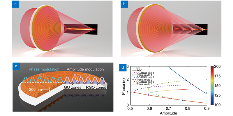
    The focusing schemes of the GO metalenses are shown in Figs. 1(a) and 1(b), in which a planewave incident light beam is focused by the GO metalenses into a super-resolved optical needle and an axial multifocal spot array, respectively. We choose these two cases because they require very accurate phase and amplitude modulations both in design and fabrication, in which the results are extremely sensitive to design/fabrication imperfections. Although the axicon for focusing an ultralong focal spot has been demonstrated by metalens before42, the linear phase modulation always causes either low focal resolution or relatively short nondiffracting distance. In addition, multifocal spots are conventionally achieved by phase plates or metasurfaces to modulate the incident beams at the back aperture of the objective lenses, where bulky high NA objective lenses are required43-48. In the meantime, the conditions for achieving multifocal arrays are even stricter, because it requires distinct constructive and destructive interference at the exact positions, otherwise, the focal spots connect with each other and cannot be well distinguished. Even though there are several demonstrations of multifocal arrays generation using metalenses29, 49, the generation of multifocal arrays using a 2D material lens has not been reported.

    The schematic demonstration of the GO metalenses is shown in Fig. 1(c), which is composed of concentric RGO rings and GO rings. The RGO rings are formed by direct femtosecond laser reduction on a uniform GO film, in which process the absorption and the refractive index increase while the thickness reduces31. In this way, the GO metalens achieves both phase and amplitude modulations simultaneously at the same position (Details of phase and amplitude modulation analysis can be seen in Methods and Supplementary Information Section S1.2). Due to near Gaussian shape intensity distribution of the fabrication laser beam, the resulted modulations show a Gaussian profile as demonstrated previously31. It has been found that the Gaussian profile is more advantageous in both focusing performance (resolutions) and diffraction efficiency31 (See theoretical analysis in Supplementary information Section S1.2).

    The phase-amplitude dependence is illustrated in Fig. 1(d). The blue line and brown line are the phase-amplitude relationships for the GO and RGO at the wavelength of 632.8 nm, respectively. Note that the maximum thickness change ( $ {\rm{\Delta}} t $) of the film depends on the initial thickness $ t $ of the GO film in the relationship of $ \max\left({\rm{\Delta}} t\right)=t/2 $ due to the change of layer spacing of graphene-based materials as demonstrated before. In the meantime, the changes of maximum refractive index ( $ {\rm{\Delta}} n $) and extinction coefficient ( $ {\rm{\Delta}} k $) are independent on the film thickness and depend only on the material properties. However, $ {\rm{\Delta}} k $ and $ {\rm{\Delta}} t $ are all decided by the reduction extent, which is eventually controlled by the laser power. Thus, $ {\rm{\Delta}} k $ and $ {\rm{\Delta}} t $ are correlated. The strategy to find out the relationship between the $ {\rm{\Delta}} n $, $ {\rm{\Delta}} k $ and $ {\rm{\Delta}} t $, is by preparing the film with a certain thickness, then reducing it with different laser powers to obtain different reduction extents32. The resulted thicknesses are measured by an atomic force microscope (AFM) and the complex refractive indexes are measured by a spectroscopic ellipsometry32. Three GO/RGO pairs are shown on the blue and brown lines (Fig. 1(d)), whose thicknesses are 200 nm/100 nm, 300 nm/150 nm, and 250 nm/125 nm, and are labelled with dot (●), cross (+), and triangle (Δ), respectively. There is a generalized square root exponential relationship between the phase-amplitude modulations if the GO to RGO transition is continuous. The transitional routes for these GO/RGO pairs are illustrated by chromatic solid line, green dash line, and purple dash line, respectively. The color bar indicates the thickness of RGO for transitional route 1, which is controlled by the laser reduction extent. These routes describe phase-amplitude dependency, which can be expressed as (Supplementary information notes S1.1)

    $ Am{p}^{2}={\rm{exp}}\left(C\cdot \textit{ϕ} \right)\;, $ (1)

    where, ϕ and Amp are the phase and amplitude of GO/RGO, respectively. C is the parametric equation of thickness $ t $. The quantitative dependency is applied in designing GO metalenses, and the GO and RGO thicknesses are chosen as 200 nm and 100 nm, which is GO/RGO pair marked with dot (●). The transitional route is the chromatic solid line shown in Fig. 1(d) with a color bar indicating the thickness.

    The position and the linewidth of each ring can be flexibly manipulated to optimize the light interference in the focal region of the incident beam. The linewidth of the rings is fixed at 400 nm, which is decided by the resolution of the laser fabrication system. Based on our quantitative phase-amplitude dependency, the optical needle lens and the multifocal lens are designed using an optimization process, in which the positions of the rings are input variables; the desired focal region optical field is the target function (see Methods).

    The designed lenses (Supplementary information Table S2 and Table S3) are fabricated by reducing the GO film with direct laser writing (DLW), the optical setup of which is shown in Fig. S4. The optical image of the multifocal lens is shown in Fig. 2(a), which has a radius of around 180 µm composing of 100 rings. By magnifying the structure with a scanning electron microscope (SEM) (Fig. 2(b)), the 400 nm linewidth by laser reduction is verified. In order to visualize the morphology of the lens, a three-dimensional (3D) optical profiler (Bruker ContourGT InMotion) (Fig. 2(c)) and an AFM (Fig. 2(d)) were used. The results indicate that the thickness is reduced, and the Gaussian like profiles resulting from the laser reduction can be clearly identified (indicated by the cross-sectional plot in Fig. 2(d)), which is similar to our design in Fig. S3(a). The maximum $ {\rm{\Delta}} t $ defined as the difference between the top and bottom in the curve is 100 nm, which exactly meets our design condition. The maximum ring radius (amax) and focal lengths for both GO metalenses are ~175 μm and 210 μm, respectively. The corresponding NA is $ {\rm{sin}}\left({\rm{arctan}}\left({a}_{{\rm{max}}}/f\right)\right) $, which equals to 0.64 for both GO metalenses. Note that the NA demonstrated here is much higher than that in most references of the metasurface lenses10, 22, 50, 51. Under this circumstance, we used the original Rayleigh-Sommerfeld theory without any approximation to calculate the focal intensity distribution52, because we have demonstrated that conventional theoretical framework based on the Fresnel approximation can no longer give precise intensity distribution in the focal region of the metalenses52.

    Characterization of GO metalens. (a) Optical image of GO metalens taken by an optical microscope with an objective of ×20, NA=0.5, the scale bar is 50 μm. (b) The zoom-in image of the up-right corner taken by an SEM, in which the scale bar is 5 μm. (c) Large-scale surface morphology of GO metalens measured by a 3D optical profiler. The scale bar is 20 μm. (d) The zoom-in image of the lower-right corner taken by an AFM. The scale bar is 4 μm.

    Figure 2.Characterization of GO metalens. (a) Optical image of GO metalens taken by an optical microscope with an objective of ×20, NA=0.5, the scale bar is 50 μm. (b) The zoom-in image of the up-right corner taken by an SEM, in which the scale bar is 5 μm. (c) Large-scale surface morphology of GO metalens measured by a 3D optical profiler. The scale bar is 20 μm. (d) The zoom-in image of the lower-right corner taken by an AFM. The scale bar is 4 μm.

    The focusing performance is characterized by a homemade imaging system (Fig. S5) consisting of a high NA objective (NA=0.8, 100×) mounted on a nanometric piezo stage and a tube lens (f = 200 mm). The intensity distribution in the focal region is captured by a high dynamic range (HDR) charge coupled device (CCD) camera. The lens is illuminated by the collimated planewave from a He-Ne laser at 632.8 nm.

    The theoretical result of the optical needle in the x-z plane is shown in Fig. 3(a), in which a needle with a subwavelength full width at half maximum (FWHM) along the lateral direction (Fig. 3(d)) covering the axial range of 16.6λ (10.5 μm) in designed (Fig. 3(c)). The corresponding experimental intensity distributions in the x-z plane and lateral FWHM are shown in Figs. 3(b) and 3(d), which fit well with the simulation results. In Fig. 3(c), both theoretical and experimental normalized intensity along the optical axis are depicted with little discrepancy. Furthermore, normalized intensities at corresponding positions shown in Figs. 3(b) (marked by the white dash lines) are demonstrated in Figs. 3(e)-3(h), and the lateral FWHMs at these positions are 0.81λ, 0.74λ, 0.73λ, 0.70λ, respectively (Fig. 3(d)). The conventional diffraction-limited lateral resolution and axial resolution are $0.5\lambda /NA = 0.78\lambda $ and $2\lambda /N{A^2} = 4.87\lambda $, respectively. Therefore, the resolution of the optical needle is beyond the conventional diffraction-limited resolution, the super-resolved light needle is achieved by exploiting the concept of supercritical focusing condition53, 54, which is defined between conventional diffraction limit and super oscillatory criterion ( $ 0.38\lambda /NA $). In our design method (detailed design process can be found in Methods and Supplementary information Section S1.2), by elongating the focal spot along the axis direction to form an optical needle, the lateral resolution beyond the diffraction limit can be achieved.

    Focusing characterization of optical needle GO metalens. (a), (b) Normalized intensity distributions in the x-z plane from theoretical calculation and experiment, respectively. (c) Theoretical and experimental normalized intensity plots along optical axial in the focal region. (d) Theoretical lateral FWHM plot along z-direction near focal region and experimental FWHM points at the positions marked by the dash lines shown in (b) at 208 μm, 210 μm, 212 μm, 214 μm respectively. (e)−(h) Normalized intensity distributions at corresponding positions shown in (d), the lateral FWHMs at these positions are 0.81 λ, 0.74 λ, 0.73 λ, 0.70 λ.

    Figure 3.Focusing characterization of optical needle GO metalens. (a), (b) Normalized intensity distributions in the x-z plane from theoretical calculation and experiment, respectively. (c) Theoretical and experimental normalized intensity plots along optical axial in the focal region. (d) Theoretical lateral FWHM plot along z-direction near focal region and experimental FWHM points at the positions marked by the dash lines shown in (b) at 208 μm, 210 μm, 212 μm, 214 μm respectively. (e)−(h) Normalized intensity distributions at corresponding positions shown in (d), the lateral FWHMs at these positions are 0.81 λ, 0.74 λ, 0.73 λ, 0.70 λ.

    In addition, the theoretical and experimental results of the axial multifocal array in the x-z plane with four nearly identical focal spots along the optical axis are shown in Figs. 4(a) and 4(b). The lateral and axial resolutions of each spot are ~0.7λ and ~4λ, respectively. The experimentally measured normalized intensity distribution along the z-direction is shown in Fig. 4(c), which agrees well with the theoretical result in the same plot. The Figs. 4(d)-4(g) show that the four focal spot distributions are smooth and nearly identical at the positions marked by dashed lines in Fig. 4(b), with lateral FWHMs of 0.97λ, 0.94λ, 0.87λ, 0.91λ, respectively. It is worth mentioning that the well-separated focal spots with uniform intensity distributions can only be achieved by accurate phase and amplitude modulations, which can be attributed to the accurate control of the complex refractive index and the thickness with the laser reduction technique. Here, with quantitative phase-amplitude dependency guiding our design and laser fabrication, we demonstrate the generation of multifocal arrays with high qualities in the case of using GO metalenses. Although some discrepancy between simulation and experiments can be seen in Fig. 3 and Fig. 4 due to the surface roughness of the as-prepared GO films (the detailed analysis can be found in Supplementary information Section S1.3), the super-resolved optical needle and overall multiple foci distribution are still reasonably well matching the simulation to verify the accuracy of our amplitude and phase dependency and the design of our GO metalenses.

    Focusing characterization of axial multifocal spots GO metalens. (a), (b) Normalized intensity distributions in the x-z plane from theoretical calculation and experiments, respectively. (c) Theoretical and experimental normalized intensity plots along the optical axial in the focal region. (d)−(g) Normalized intensity distributions at positions marked by the dashed lines shown in (b), the axial positions are 202 μm, 206 μm, 212 μm, 218 μm. The lateral FWHMs at these positions are 0.97 λ, 0.94 λ, 0.87 λ, 0.91 λ.

    Figure 4.Focusing characterization of axial multifocal spots GO metalens. (a), (b) Normalized intensity distributions in the x-z plane from theoretical calculation and experiments, respectively. (c) Theoretical and experimental normalized intensity plots along the optical axial in the focal region. (d)−(g) Normalized intensity distributions at positions marked by the dashed lines shown in (b), the axial positions are 202 μm, 206 μm, 212 μm, 218 μm. The lateral FWHMs at these positions are 0.97 λ, 0.94 λ, 0.87 λ, 0.91 λ.

    It is noteworthy that the GO metalenses are thicker than the metasurface designs based on metal structure. However, as metals are general lossy materials in visible range, the efficiency of the metal based design is limited to around 1%42, which is relatively low. On the other hand, the recent development of dielectric metasurface can significantly improve the focusing efficiency, however, the thickness of the metasurface needs to be several hundred nanometers, which is typically near the effective wavelength λeff of the incident light. Compared with the dielectric metasurface, our 200 nm metalenses are thinner due to the achievement of subwavelength thickness by applying both phase and amplitude modulations. In our GO metalenses, the effective wavelength of the 632.8 nm laser in the GO material is 351.6 nm. In addition, overall focusing efficiency is defined as the ratio of total power in a circular aperture with the size three times of the FWHM of the focal spot to the total power of the transmitted light through the lens55, which is around 10%. Considering the amplitude modulation giving a transmission around 70%, the focusable energy compared with the energy immediately after amplitude and phase modulations is around 15%. The loss is mainly due to the zero-order transmission and the -1 order diffraction, which do not contribute to the focus. The efficiency can be further improved by introducing different modulation levels into the design that minimize the zero and -1 orders, which is feasible by controlling the laser power. As demonstrated in our previous work, up to 8 modulation levels can be obtained in the GO/RGO system32, 35.

    In our previous work we have proved that by using the simultaneous phase and amplitude modulations provided by photo-reduction of GO materials56, it is possible to focus optical energy with subwavelength resolution31. In this work, we further build the relationship between the amplitude and phase modulations to design the GO metalens to show advanced functionalities, such as an optical needle, and a multifocal array, which are quite challenging for any metalenses. Since the analytical design method used in our previous work cannot be applied to generate advanced focal field distributions, we further developed an optimization method, which is able to provide sophisticated control to achieve the required lens designs. Compared with phase or amplitude modulation only metasurfaces, the simultaneous phase and amplitude modulations of the GO/RGO material system provide further flexibility to the design method. The successful demonstrations of the optical needle and the multifocal array not only prove the effectiveness of the design method, but also confirm the accurate phase and amplitude controls can be achieved in experiments. Therefore, combining the design method and experimental fabrication technique, it is possible to further demonstrate GO metalenses with different functionalities, thus broad applications.

    Conclusion

    In conclusion, based on the unique optical properties of graphene-based materials (GO and RGO) under laser illumination, including the complex refractive index and the thickness change, we build up the quantitative phase-amplitude dependency, which provides a well-guided design process for photonic devices based on graphene-based materials with simultaneous amplitude and phase modulations at a single position. By understanding the phase-amplitude dependency, we are able to design photonic devices with a high accuracy. To validate the accuracy of our GO metalens design strategy, we experimentally demonstrated GO metalenses, which generate an ultra-long (~16λ) super-resolved optical needle and an axial multifocal array (4 focal spots) as examples. Although we have demonstrated only two designs in the study, the phase-amplitude dependency can be further applied to design other photonic devices such as optical chain, optical cage, optical bubble and optical tweezers for the applications in optical trapping, optical manipulating, optical delivering and optical staking47, 57-59.

    Due to the flexibility and mechanical robustness of graphene-based materials as well as the simple, low-cost, and scalable fabrication of GO metalenses, these ultrathin flat optical components enable great potential in applications and possess commercial value in integrated optical device33, 60. Compared with the conventional nanofabrication techniques such as EBL and FIB, which are required for the fabrication of metasurfaces, the DLW technique is able to in-situ fabricate lens in a single step. The attributes of large-scale, long working distance, high lateral resolution and desired longitudinal morphology constitute a milestone that optical manipulation, portable microscope, parallel optical processing and high-density optical data storage can be realized in an integrated setup without the requirement of bulky optical elements43-46, 48, 61.

    Methods

    Preparation of GO film

    The ~200 nm homogeneous GO film was prepared using the vacuum filtration method with high quality GO solution synthesized by the modified Hummer’s method62, and then was transferred onto a cover glass.

    Lens design and optimization

    The designs of the optical needle lens and the multifocal lens are based on the powerful interior-point optimization algorithm63. The target functions for optical needle and multifocal lenses are given by Eq. (1) and Eq. (2), respectively.

    $ \begin{split} & {I}_{{\rm{needle}}}\left(z\right)=\\& \left\{\!\!\!\begin{array}{l}1,\; 205.73\;{\mu\rm{m}} \le z\le 215.22\;{\mu\rm{m}} \left(325\lambda \le z\le 340\lambda \right)\\ 0,\; {\rm{otherwise}}\end{array}\right. \end{split},$ (2)

    where, ${I}_{{\rm{needle}}}\left(z\right)$ is a rectangle function along the Z axis defined from 189.90 μm (300λ) to 227.88 μm (360λ).

    $ {I}_{{\rm{multifoci}}}\left(z\right)=\sum\limits _{i=1}^{4}1-\left|\frac{1}{{t}_{0}}\left(z-{z}_{i}\right)\right| \;.$ (3)

    The target function of multifoci is a summation of triangular function along the Z axis defined from 189.90 μm (300λ) to 227.88 μm (360λ). ${t_0}$ equals to 5λ, which also defines the FWHM of multifoci. ${z_i}$ are peak positions, which are 315λ, 325λ, 335λ, and 345λ, respectively. The optimum designs have minimal variances between the actual field distributions and the merit functions. The electrical fields diffracted by the circularly symmetric lens illuminated by the planewave can be described by Rayleigh-Sommerfeld diffraction theory64. The electrical field at position (r=0, z=f) is given by65:

    $ \begin{split} & E\left( {{r} = 0,z = f} \right) \\ & \qquad = \int\limits_0^{{a_{\max}}} {E_0}\left( {{r_1},z = 0} \right)r\frac{{\,{\rm{exp}} \, \left( {{\rm{i}}k\sqrt {{z^2} + {r_1}^2} } \right)}}{{{z^2} + {r_1}^2}}\\ & \qquad\times \left( {{\rm{i}}k - \frac{1}{{\sqrt {{z^2} + {r_1}^2} }}} \right){\rm{d}}r_1\;,\\ & {E_0}\left( {{r_1},z = 0} \right) \\ & \qquad= \left\{\!\! {\begin{array}{*{20}{l}} {{A_{{\rm{GO}}}}\,{{\rm{exp}}} \, \left( {{\rm{i}}{\phi _{{\rm{GO}}}}} \right),\;{\rm{without}}\;{\rm{laser}}\;{\rm{reduction}}}\\ {{A_{\rm{T}}}\,{{\rm{exp}}} \,\left( {{\rm{i}}{\phi _{\rm{T}}}} \right),\;{\rm{with}}\;{\rm{laser}}\;{\rm{reduction}}} \end{array}}, \right.\\ & \qquad\qquad \qquad I = {\rm{abs}}{\left( E \right)^2}\;,\\[-11pt] \end{split} $  (4)

    where, amax is the radius of the largest ring, k is the wavenumber. AGO and φGO are the amplitude and phase modulations for GO in our design, respectively. Meanwhile, AT and φT are the amplitude and phase modulations of RGO zones, which obey our GO phase-amplitude dependency (chromatic transitional route 1 in Fig. 1(b)). The intensity at the focal point is the square of the absolute value of the electric field.

    The constrains of the optimization are shown in Eq. (5):

    $\left\{ \begin{array}{*{20}{l}} {{a_{m + 1}} - {a_m} > l}\\ {{a_1} > d}\\ {{NA} \ge N{A_{\min }}} \end{array}\right. \;,$  (5)

    where, ${a_m}$ are the ring positions for RGO. l denotes the minimum distance between the adjacent two rings, which is 1.0 μm. d is the minimum radius requirement for the first ring, which is set to be 0.8 μm. $N{A_{\min }}$ is the minimum NA requirement in the optimization, which is set to be 0.6 for both multifocal lens and optical needle lens. For the sake of experimental fabrication accuracy, the width of all rings is set to be 400 nm. Moreover, the maximum phase modulation caused by the RGO and GO film is calculated to be -0.1700π; the minimal transmittance of rings is set to be 0.3539; the working wavelength of the metalenses is 632.8 nm.

    Femtosecond laser fabrication

    With a commercial laser 3D nanoprinting setup (Special Edition, Innofocus Nanoprint3D) (Fig. S4), the laser reduction process was performed on our as-prepared GO film according to the radii in supplementary information Tables 1 and 2. The femtosecond laser beam (100 fs pulse, 100 kHz, 800 nm) with a fabrication speed at 30 μm/s was calibrated at 12 μW for reducing the GO film, which is mounted on a 3D nanometric piezo stage (Physik Instrumente). A high NA oil objective (NA=1.4, 100×) is used in fabrication. The lateral resolution of laser fabrication on GO thin film is determined by the size of femtosecond laser focal spot and the laser interaction threshold with the GO material. The FWHM of the laser focal spot is determined by $ \lambda /2NA $, where $ \lambda $ is the wavelength of the writing laser and $ NA $ is the numerical aperture of the writing objective lens. In our case, laser wavelength is 800 nm, $ NA $ is 1.4. Thus, the laser resolution is around 300 nm. In the direct laser fabrication of GO lenses, the linewidth is approximately 400 nm, due to the selection of laser power and the laser interaction threshold with the GO material.

    References

    [1] A Arbabi, E Arbabi, SM Kamali, Y Horie, S Han, et al. Miniature optical planar camera based on a wide-angle metasurface doublet corrected for monochromatic aberrations. Nat Commun, 7, 13682(2016).

    [2] B Groever, WT Chen, F Capasso. Meta-lens doublet in the visible region. Nano Lett, 17, 4902-4907(2017).

    [3] M Farmahini-Farahani, JR Cheng, H Mosallaei. Metasurfaces nanoantennas for light processing. J Opt Soc Am B, 30, 2365-2370(2013).

    [4] NF Yu, F Aieta, P Genevet, MA Kats, Z Gaburro, et al. A broadband, background-free quarter-wave plate based on plasmonic metasurfaces. Nano Lett, 12, 6328-6333(2012).

    [5] XQ Zhang, Z Tian, WS Yue, JQ Gu, S Zhang, et al. Broadband terahertz wave deflection based on c-shape complex metamaterials with phase discontinuities. Adv Mater, 25, 4567-4572(2013).

    [6] P Genevet, NF Yu, F Aieta, J Lin, MA Kats, et al. Ultra-thin plasmonic optical vortex plate based on phase discontinuities. Appl Phys Lett, 100, 013101(2012).

    [7] MA Kats, P Genevet, G Aoust, NF Yu, R Blanchard, et al. Giant birefringence in optical antenna arrays with widely tailorable optical anisotropy. Proc Natl Acad Sci USA, 109, 12364-12368(2012).

    [8] F Monticone, NM Estakhri, A Alù. Full control of nanoscale optical transmission with a composite metascreen. Phys Rev Lett, 110, 203903(2013).

    [9] C Pfeiffer, A Grbic. Metamaterial huygens' surfaces: tailoring wave fronts with reflectionless sheets. Phys Rev Lett, 110, 197401(2013).

    [10] NF Yu, P Genevet, MA Kats, F Aieta, JP Tetienne, et al. Light propagation with phase discontinuities: generalized laws of reflection and refraction. Science, 334, 333-337(2011).

    [11] K Keskinbora, C Grévent, M Bechtel, M Weigand, E Goering, et al. Ion beam lithography for Fresnel zone plates in X-ray microscopy. Opt Express, 21, 11747-11756(2013).

    [12] T Jwad, SA Deng, H Butt, S Dimov. Fabrication of TiO2 thin film-based fresnel zone plates by nanosecond laser direct writing. J Micro Nano-Manuf, 6, 011001(2018).

    [13] D Bowman, TL Harte, V Chardonnet, Groot De, SJ Denny, et al. High-fidelity phase and amplitude control of phase-only computer generated holograms using conjugate gradient minimisation. Opt Express, 25, 11692-11700(2017).

    [14] GY Lee, G Yoon, SY Lee, H Yun, J Cho, et al. Complete amplitude and phase control of light using broadband holographic metasurfaces. Nanoscale, 10, 4237-4245(2018).

    [15] LX Liu, XQ Zhang, M Kenney, XQ Su, NN Xu, et al. Broadband metasurfaces with simultaneous control of phase and amplitude. Adv Mater, 26, 5031-5036(2014).

    [16] Q Wang, XQ Zhang, YH Xu, JQ Gu, YF Li, et al. Broadband metasurface holograms: toward complete phase and amplitude engineering. Sci Rep, 6, 32867(2016).

    [17] G Yoon, D Lee, KT Nam, J Rho. “Crypto-display” in dual-mode metasurfaces by simultaneous control of phase and spectral responses. ACS Nano, 12, 6421-6428(2018).

    [18] C Pfeiffer, C Zhang, V Ray, LJ Guo, A Grbic. High performance bianisotropic metasurfaces: asymmetric transmission of light. Phys Rev Lett, 113, 023902(2014).

    [19] ML Tseng, HH Hsiao, CH Chu, MK Chen, G Sun, et al. Metalenses: advances and applications. Adv Opt Mater, 6, 1800554(2018).

    [20] J Engelberg, U Levy. The advantages of metalenses over diffractive lenses. Nat Commun, 11, 1991(2020).

    [21] SM Wang, PC Wu, VC Su, YC Lai, MK Chen, et al. A broadband achromatic metalens in the visible. Nat Nanotechnol, 13, 227-232(2018).

    [22] RH Lin, XH Li. Multifocal metalens based on multilayer pancharatnam-berry phase elements architecture. Opt Lett, 44, 2819-2822(2019).

    [23] ML Tseng, YW Huang, MK Hsiao, HW Huang, HM Chen, et al. Fast fabrication of a Ag nanostructure substrate using the femtosecond laser for broad-band and tunable plasmonic enhancement. ACS Nano, 6, 5190-5197(2012).

    [24] CH Chu, ML Tseng, Shiue da, SW Chen, HP Chiang, et al. Fabrication of phase-change Ge2Sb2Te5 nano-rings. Opt Express, 19, 12652-12657(2011).

    [25] N Lassaline, R Brechbühler, SJW Vonk, K Ridderbeek, M Spieser, et al. Optical fourier surfaces. Nature, 582, 506-510(2020).

    [26] KTP Lim, HL Liu, YJ Liu, JKW Yang. Holographic colour prints for enhanced optical security by combined phase and amplitude control. Nat Commun, 10, 25(2019).

    [27] WH Yang, SM Xiao, QH Song, YL Liu, YK Wu, et al. All-dielectric metasurface for high-performance structural color. Nat Commun, 11, 1864(2020).

    [28] M Semmlinger, ML Tseng, J Yang, M Zhang, C Zhang, et al. Vacuum ultraviolet light-generating metasurface. Nano Lett, 18, 5738-5743(2018).

    [29] BH Chen, PC Wu, VC Su, YC Lai, CH Chu, et al. GaN metalens for pixel-level full-color routing at visible light. Nano Lett, 17, 6345-6352(2017).

    [30] XW Chen, X Hai, JH Wang. Graphene/graphene oxide and their derivatives in the separation/isolation and preconcentration of protein species: a review. Anal Chim Acta, 922, 1-10(2016).

    [31] XR Zheng, BH Jia, H Lin, L Qiu, D Li, et al. Highly efficient and ultra-broadband graphene oxide ultrathin lenses with three-dimensional subwavelength focusing. Nat Commun, 6, 8433(2015).

    [32] YY Yang, H Lin, BY Zhang, YN Zhang, XR Zheng, et al. Graphene-based multilayered metamaterials with phototunable architecture for on-chip photonic devices. ACS Photonics, 6, 1033-1040(2019).

    [33] TS Yang, H Lin, XR Zheng, KP Loh, BH Jia. Tailoring pores in graphene-based materials: from generation to applications. J Mater Chem A, 5, 16537-16558(2017).

    [34] CL Hao, ZQ Nie, HP Ye, H Li, Y Luo, et al. Three-dimensional supercritical resolved light-induced magnetic holography. Sci Adv, 3, e1701398(2017).

    [35] H Lin, BCP Sturmberg, KT Lin, YY Yang, XR Zheng, et al. A 90-nm-thick graphene metamaterial for strong and extremely broadband absorption of unpolarized light. Nat Photonics, 13, 270-276(2019).

    [36] GY Cao, H Lin, S Fraser, XR Zheng, Rosal Del, et al. Resilient graphene ultrathin flat lens in aerospace, chemical, and biological harsh environments. ACS Appl Mater Interfaces, 11, 20298-20303(2019).

    [37] PP Mondal, A Diaspro. Simultaneous multilayer scanning and detection for multiphoton fluorescence microscopy. Sci Rep, 1, 149(2011).

    [38] XP Li, YY Cao, M Gu. Superresolution-focal-volume induced 3.0 Tbytes/disk capacity by focusing a radially polarized beam. Opt Lett, 36, 2510-2512(2011).

    [39] JM Auñón, CW Qiu, M Nieto-Vesperinas. Tailoring photonic forces on a magnetodielectric nanoparticle with a fluctuating optical source. Phys Rev A, 88, 043817(2013).

    [40] J Godin, CH Chen, SH Cho, W Qiao, F Tsai, et al. Microfluidics and photonics for bio-system-on-a-chip: a review of advancements in technology towards a microfluidic flow cytometry chip. J Biophotonics, 1, 355-376(2008).

    [41] M Born, E Wolf. Principles of Optics: Electromagnetic Theory of Propagation, Interference and Diffraction of Light(1999).

    [42] F Aieta, P Genevet, MA Kats, NF Yu, R Blanchard, et al. Aberration-free ultrathin flat lenses and axicons at telecom wavelengths based on plasmonic metasurfaces. Nano Lett, 12, 4932-4936(2012).

    [43] G Mínguez-Vega, J Lancis, J Caraquitena, V Torres-Company, P Andrés. High spatiotemporal resolution in multifocal processing with femtosecond laser pulses. Opt Lett, 31, 2631-2633(2006).

    [44] H Lin, BH Jia, M Gu. Dynamic generation of debye diffraction-limited multifocal arrays for direct laser printing nanofabrication. Opt Lett, 36, 406-408(2011).

    [45] M Gu, H Lin, XP Li. Parallel multiphoton microscopy with cylindrically polarized multifocal arrays. Opt Lett, 38, 3627-3630(2013).

    [46] H Lin, M Gu. Creation of diffraction-limited non-Airy multifocal arrays using a spatially shifted vortex beam. Appl Phys Lett, 102, 084103(2013).

    [47] LW Zhu, JJ Yu, DW Zhang, MY Sun, JN Chen. Multifocal spot array generated by fractional Talbot effect phase-only modulation. Opt Express, 22, 9798-9808(2014).

    [48] ZQ Nie, H Lin, XF Liu, AP Zhai, YT Tian, et al. Three-dimensional super-resolution longitudinal magnetization spot arrays. Light Sci Appl, 6, e17032(2017).

    [49] XF Zang, HZ Ding, Y Intaravanne, L Chen, Y Peng, et al. A multi-foci metalens with polarization-rotated focal points. Laser Photon Rev, 13, 1900182(2019).

    [50] MQ Mehmood, H Liu, K Huang, ST Mei, A Danner, et al. Broadband spin-controlled focusing via logarithmic-spiral nanoslits of varying width. Laser Photonics Rev, 9, 674-681(2015).

    [51] MY Li, WL Li, HY Li, YC Zhu, YT Yu. Controllable design of super-oscillatory lenses with multiple sub-diffraction-limit foci. Sci Rep, 7, 1335(2017).

    [52] GY Cao, XS Gan, H Lin, BH Jia. An accurate design of graphene oxide ultrathin flat lens based on Rayleigh-Sommerfeld theory. Opto-Electron Adv, 1, 180012(2018).

    [53] K Huang, HP Ye, JH Teng, SP Yeo, B Luk’yanchuk, et al. Optimization-free superoscillatory lens using phase and amplitude masks. Laser Photonics Rev, 8, 152-157(2014).

    [54] K Huang, F Qin, H Liu, HP Ye, CW Qiu, et al. Planar diffractive lenses: fundamentals, functionalities, and applications. Adv Mater, 30, 1704556(2018).

    [55] A Arbabi, Y Horie, AJ Ball, M Bagheri, A Faraon. Subwavelength-thick lenses with high numerical apertures and large efficiency based on high-contrast transmitarrays. Nat Commun, 6, 7069(2015).

    [56] XP Li, HR Ren, X Chen, J Liu, Q Li, et al. Athermally photoreduced graphene oxides for three-dimensional holographic images. Nat Commun, 6, 6984(2015).

    [57] XY Weng, LP Du, P Shi, XC Yuan. Tunable optical cage array generated by Dammann vector beam. Opt Express, 25, 9039-9048(2017).

    [58] SH Xu, YM Li, LR Lou. Axial optical trapping forces on two particles trapped simultaneously by optical tweezers. Appl Opt, 44, 2667-2672(2005).

    [59] YQ Zhao, QW Zhan, YL Zhang, YP Li. Creation of a three-dimensional optical chain for controllable particle delivery. Opt Lett, 30, 848-850(2005).

    [60] XR Zheng, H Lin, TS Yang, BH Jia. Laser trimming of graphene oxide for functional photonic applications. J Phys D Appl Phys, 50, 074003(2017).

    [61] YB Ma, GH Rui, B Gu, YP Cui. Trapping and manipulation of nanoparticles using multifocal optical vortex metalens. Sci Rep, 7, 14611(2017).

    [62] Jr Hummers, RE Offeman. Preparation of graphitic oxide. J Amer Chem Soc, 80, 1339(1958).

    [63] SP Boyd, L Vandenberghe. Convex Optimization(2004).

    [64] M Gu. Advanced Optical Imaging Theory(2000).

    [65] HP Ye, CW Qiu, K Huang, JH Teng, B Luk’yanchuk, et al. Creation of a longitudinally polarized subwavelength hotspot with an ultra-thin planar lens: vectorial Rayleigh-Sommerfeld method. Laser Phys Lett, 10, 065004(2013).

    Acknowledgements

    H. T. Wang acknowledges the support from National Key Research and Development Program of China (2017YFB0403602) and China Scholarship Council. B. H. Jia acknowledges the support from the Australian Research Council through the Discovery Projects (DP150102972, DP190103186), the Industrial Transformation Training Centres scheme (Grant No. IC180100005) and support from Defence Science Institute (DSI) and Defence Science and Technology Group (DSTG). C. W. Qiu acknowledges the support from the National Research Foundation, Prime Minister’s Office, Singapore, under its Competitive Research Programme (CRP award NRF CRP22-2019-0006), Advanced Research and Technology Innovation Centre (ARTIC) under the grant (R-261-518-004-720), and A*STAR under Advanced Manufacturing and Engineering (AME) Individual Research Grant (IRG A2083c0060). T. Lan acknowledges National Key Basic Research Program 973 Project (2013CB329202). National Major Scientific Instruments and Equipments Development Project supported by National Natural Science Foundation of China (No. 61827814).

    Author contributions

    B. H. Jia, H. Lin and C. W. Qiu conceived the idea and developed the strategy of the project. C. L. Hao and C. W. Qiu, developed the optimization algorithm, and designed the lens parameters. H. T. Wang conducted the GO film preparing, GO lens fabrication, GO lens characterization and focused light fields measurements. B. H. Jia, H. Lin and H. T. Wang contributed to data analysis. H. T. Wang and C. L. Hao drafted the manuscript. All authors discussed and commented on the manuscript.

    Competing interests

    The authors declare no competing financial interests.

    Supplementary information

    Supplementary information for this paper is available at https://doi.org/10.29026/oea.2021.200031
    Hongtao Wang, Chenglong Hao, Han Lin, Yongtian Wang, Tian Lan, Cheng-Wei Qiu, Baohua Jia. Generation of super-resolved optical needle and multifocal array using graphene oxide metalenses[J]. Opto-Electronic Advances, 2021, 4(2): 200031-1
    Download Citation