Author Affiliations
1Engineering Research Center of Optical Instrument and Systems, Ministry of Education and Shanghai Key Laboratory of Modern Optical System, University of Shanghai for Science and Technology, Shanghai 200093, China2Department of Materials Science and Engineering, City University of Hong Kong, Hong Kong, China3Shanghai Institute of Intelligent Science and Technology, Tongji University, Shanghai 200092, China4e-mail: jwen@usst.edu.cn5e-mail: dwzhang@usst.edu.cnshow less
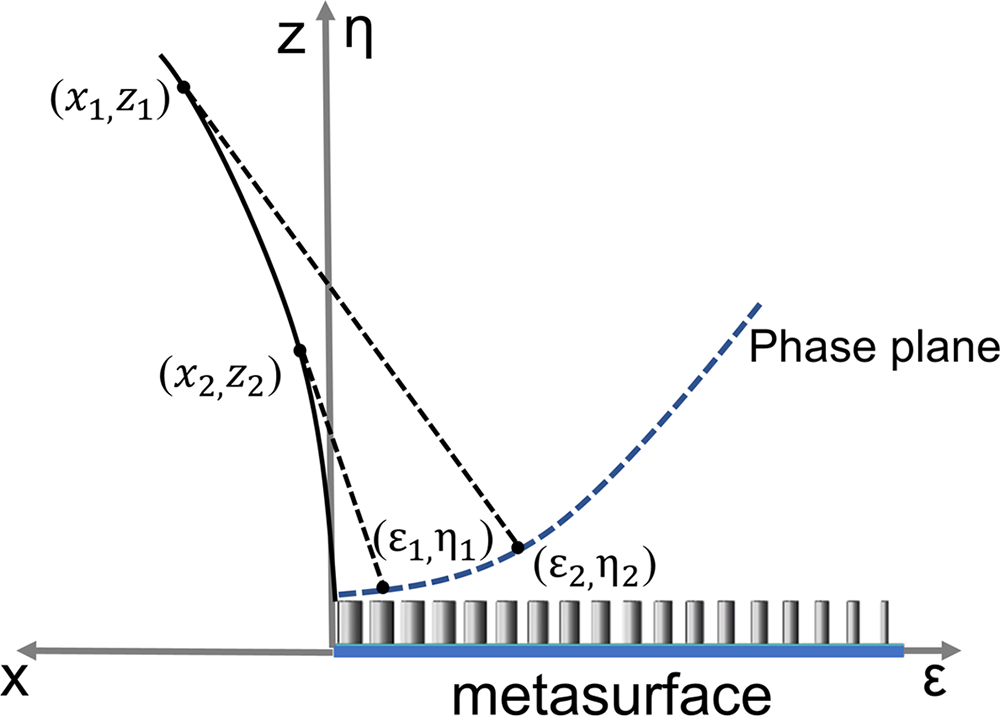
Fig. 1. Geometrical model for generating Airy optical beams with a metasurface.
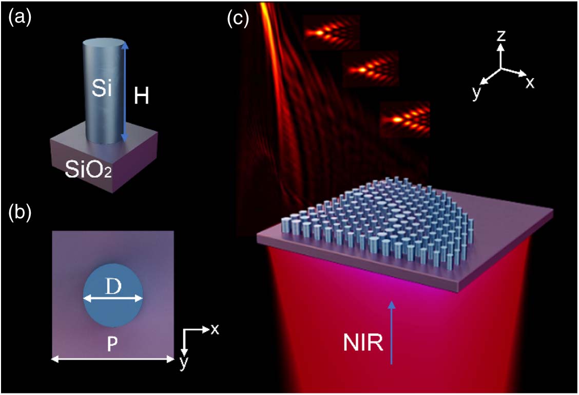
Fig. 2. (a) Schematic side and (b) top views of an amorphous silicon nanopillar unit with height H, diameter D, and lattice constant P on an SiO2 substrate; (c) the dielectric metasurface, composed of the above silicon nanopillars with spatially varied diameters, is imposed by a 3/2 phase for Airy optical beam generation operating under transmission mode in the near-infrared (NIR) region. Experimentally measured longitudinal and transverse field distributions at different vertical planes are superimposed on top of the metasurface.
Fig. 3. (a) Simulated phase and (b) transmission intensity of an array of silicon nanopillars as a function of their diameter D. The lattice constant of the array is P=620 nm, and the height of the pillars is H=600 nm.
Fig. 4. (a) A 3/2 phase pattern imposed on the metasurface; (b) simulated longitudinal field distribution profiles of the generated Airy optical beam from the position of z=50 μm to z=105 μm along the beam deflection direction; (c)–(f) simulated transverse field distribution profiles in the xy planes at z=70 μm, 80 μm, 90 μm, and 100 μm away from the metasurface.
Fig. 5. (a) Top and (b) zoomed view SEM images of the fabricated metasurface sample; (c) schematic diagram of optical characterization setup.
Fig. 6. (a)–(f) Simulated and (g)–(l) experimental transverse xy field patterns at the position of z=87 μm when the incident beam is LP with a polarization angle of (a), (g) 0° and (b), (h) 45°, (c), (i) left circularly polarized (LCP), (d), (j) right circularly polarized (RCP), EP with an ellipticity of (e), (k) −0.5 and (f), (l) 0.5, respectively.
Fig. 7. Experimentally measured FWHM of the main lobe of each Airy beam along its propagation trajectory when the incident beam is LP with a polarized angle of 0° and 45°, LCP, RCP, and EP with an ellipticity of −0.5 and 0.5, respectively.
Fig. 8. (a)–(f) Simulated and (g)–(l) experimental longitudinal field distribution profiles of the Airy beams in the yz plane at vertical positions from z=30 μm to z=100 μm when the incident beam is LP with a polarized angle of (a), (g) 0° and (b), (h) 45°, (c), (i) LCP, (d), (j) RCP, and EP with an ellipticity of (e), (k) −0.5 and (f), (l) 0.5, respectively.
Fig. 9. (a) Simulated longitudinal field distribution profiles of the Airy beam. A sphere obstacle with a diameter of 20 μm is placed at (x,z)=(−4.1,60) μm. (b) Experimental longitudinal field distribution profiles of the Airy beam. The yellow dashed lines show the position of the thin plastic film with a microink droplet placed at z=63 μm from the metasurface.
References | Efficiency (%) | Material | Wavelength | Incident Light | Our result | 56 | Silicon | 1550 nm | Polarization-insensitive | [61] | 70–85 (simulation result, no experiment) | Silicon | 1500 nm | Polarization-insensitive | [72] | | Silver | 633 nm | Polarization-insensitive | [56] | | Gold | 2000 nm | CP light | [60] | | Gold | 780 nm | CP light | [70] | 63 | Silicon | 600–695 nm | CP light | [71] | 65–75 | Titanium dioxide | 430 nm | CP light | [55] | 13.5 (), 4.2() | Gold | 800–1100 nm | LP light | [57] | 100 (theoretical result) | Aluminum | 21.74 mm | LP light | [58] | | Aluminum | 400 μm, 750 μm | LP light |
|
Table 1. Summary of Our Result and Other References