1Photonics Research Group, Department of Information Technology, Center for Nano and Biophotonics, Ghent University imec, Ghent B-9000, Belgium
2Department of Information Technology, Internet Based Communication Networks and Services (IBCN), Ghent University iMinds, Gaston Crommenlaan 8 Bus 201, B-9050 Gent, Belgium
We demonstrate the use of stochastic collocation to assess the performance of photonic devices under the effect of uncertainty. This approach combines high accuracy and efficiency in analyzing device variability with the ease of implementation of sampling-based methods. Its flexibility makes it suitable to be applied to a large range ofphotonic devices. We compare the stochastic collocation method with a Monte Carlo technique on a numerical analysis of the variability in silicon directional couplers.
Integrated photonics, and in particular, silicon photonics, is rapidly enabling complex photonic functions on a chip [1]. However, variability due to fabrication processes and operational conditions limits the complexity of the circuits that can be implemented [2,3]. A proper analysis of the effects of the variability in geometrical, electrical, and optical parameters on the performance of the photonic building blocks and circuits has become crucial. Indeed, the variability introduced by the variations of the manufacturing process is a primary source of degradation of larger photonic circuits, especially when wavelength-selective filters are implemented [4]. The primary functional parameters that are affected are the waveguide propagation constants (the effective index) and the coupling coefficients in coupling structures. The Monte Carlo (MC) method [5] is considered the standard approach for variability analysis, thanks to its accuracy and ease of implementation. Unfortunately, the MC analysis has a slow convergence rate, and it requires a large number of data points (simulations or measurements). Therefore, MC has a high computational cost, considering that accurate simulations of photonic devices can be time and resource intensive.
The generalized polynomial chaos (gPC) expansion has been applied in several domains as an efficient alternative to the classic MC method [6–8], and, recently, it has been proposed for the variability analysis of photonic devices [9,10].
The gPC-based modeling approach aims at expressing a stochastic process as a series of orthogonal basis functions with suitable coefficients and gives an analytical representation of the variability of the system on the random variables under consideration [11].
Sign up for Photonics Research TOC. Get the latest issue of Photonics Research delivered right to you!Sign up now
In this paper, we propose a stochastic collocation (SC) method as an efficient alternative to characterize photonic devices under the effect of uncertainty. The fundamental principle of the SC approach is to approximate the unknown stochastic solution by interpolation functions in the stochastic space. The interpolation is constructed by repeatedly solving (sampling) the deterministic problem at a predetermined set of nodes in the stochastic space. This approach offers similar high accuracy and efficiency as the stochastic gPC method, but, at the same time, it is easy to implement, such as sampling-based methods (e.g., MC approach).
We apply the SC method to analyze the variability of a key building block for silicon photonic circuits: the directional coupler (DC). This device is essential in the construction of wavelength filters, as it implements an arbitrary fractional power coupling, but, at the same time, it is extremely sensitive to fabrication variations: a small shift in linewidth or thickness of the core can dramatically change the coupling coefficients.
The paper is organized as follows: Section 2 gives a general introduction of SC methods. It provides the essential mathematics knowledge that readers need to know to understand its application in the photonic domain. Section 3 uses a DC as an example to test the performance of SC in performing variability analysis of photonic devices. Section 4 draws the conclusions.
2. STOCHASTIC COLLOCATION METHODS
SC methods are based on interpolation schemes to compute stochastic quantities. The interpolation is constructed by repeatedly solving (sampling) the deterministic problem at a predetermined set of nodes in the stochastic space [12] (also defined as collocation points). Indeed, a stochastic process can be expressed as where denotes the stochastic parameters and represents the interpolation basis functions.
For a photonic device, the process could correspond to the functional parameters such as the waveguide propagating constants and the coupling coefficients in coupling devices. The stochastic variables correspond to device properties affected in a stochastic way by fabrication and operational conditions (e.g., waveguide line, width, or temperature).
In Eq. (1), different types of interpolation schemes can be adopted (e.g., piecewise linear [12,13], Lagrange [11,14], or interpolation methods that belong to the general class of positive interpolation operators such as multivariate simplicial methods [15]). However, the key issue for this approach is the selection of the support nodes, such that when using the minimal number of nodes one achieves good approximation.
For example, if the Lagrange interpolation scheme is chosen, the element in Eq. (1) for a 1D interpolation can be expressed as where is equal to 1 for and is equal to 0 for . Next, for interpolation in multiple dimensions, a tensor-product approach can be used, and Eq. (1) becomes where is the -th node in the -th direction, and the total number of nodes used in Eq. (3) is As can be seen in Eq. (4), the number of nodes required by the full tensor product increases rapidly with the number of random parameters . For example, if three random variables are considered and 10 collocation points are used for each parameter, a total of 1000 nodes are required by the full tensor product approach. Hence, the performance of the photonic device under study must be evaluated for 1000 different combinations of the random variables considered, leading to an expensive computational time.
The required number of nodes can be significantly reduced by adopting sparse grids in the stochastic space, based on the Smolyak algorithm [12,16–19]. By choosing the collocation points correctly, the Smolyak algorithm drastically reduces the total number of nodes used in the interpolation with respect to the full tensor product approach while preserving a high level of accuracy.
It is important to remark that the SC models are expanded using interpolation functions of independent random variables [11]. In the general case of correlated random variables, decorrelation can be obtained via a variable transformation, such as the Nataf transformation [20] or the Karhunen–Loéve expansion [21].
The stochastic moments (mean, variance, …) can be computed utilizing analytical formulas and then efficiently, once the analytical form of the interpolation functions has been decided. For example, if the random variables are defined in the sample space , the mean of is defined as where is the joint probability density function (PDF) of the random variables . Using Eq. (1) in Eq. (5) leads to which depends only on the interpolation functions and joint PDF . Note that, if the choice of the interpolation functions and probability measure does not allow an analytical computation of the stochastic moments like Eq. (6), an efficient numerical solution can be used (e.g., by MC analysis of the interpolation model or numerical integration). Finally, it is important to remark that it is not possible to define a priori the speed-up of a generic SC modeling technique compared with the MC method. Indeed, the number of nodes needed to compute an accurate SC model (which is directly related to the efficiency of SC methods, as described above) cannot be decided upfront because it depends on the following factors:
the impact of the chosen random variables on the variations of the stochastic process considered (dynamic stochastic processes require a higher number of collocation points);
the interpolation scheme adopted (the more powerful the interpolation scheme, the fewer nodes are needed);
the sampling strategy adopted (efficient sampling strategy limit the number of collocation points used);
the number of random variables considered (the higher the number of variables the more collocation points are needed).
However, it has been proven in the literature that, for a limited number of random variables (indicatively less than 10) SC methods are much more efficient with respect to the MC analysis (see [11,12,14]). For stochastic processes depending on a high number of random variables, the efficiency of SC methods is significantly reduced.
Two approaches can be used to increase the efficiency of an SC modeling technique. Using nested sampling schemes allows us to adaptively choose the collocation points (additional details are provided in Section 3.E and Appendix 5.B). Adopting adaptive sparse grids [16] reduces the nodes requirement, which is especially useful when a high number of random variables is considered. For a more detailed reference on SC methods, we refer the reader to [11,12,14,16].
3. DIRECTIONAL COUPLER EXAMPLE
A. Benchmark Description
We demonstrate the use of SC for integrated photonics through the analysis of a DC in a silicon photonics platform. Silicon photonics is rapidly gaining adoption due to its potential for large-scale integration and volume manufacturing. [22]. However, the same high-index contrast that enables dense integration also makes silicon photonic waveguides extremely sensitive to small imperfections in their geometry. Also, the high thermo-optic coefficient of silicon makes silicon photonic devices temperature sensitive. For instance, a change in linewidth and thickness of waveguide would noticeably vary the effective index () of optical modes, resulting in a shift of 1 nm in the response of a wavelength-selective filter. This variation leads to performance degradation in devices such as DCs, Mach–Zehnder interferometers (MZIs) and ring resonators, and limits the number of devices that a single circuit can have.
Power coupling devices are essential parts for splitting and combining power in photonic circuits. Among them, DCs are widely used for their simplicity in layout and easy-to-understand operation. An advantage of DCs compared with other couplers is that the coupling ratio can be continuously adjusted by choosing the length of the coupling section. Furthermore, DCs constitute the building blocks of many larger photonic devices such as rings, MZIs, and so on.
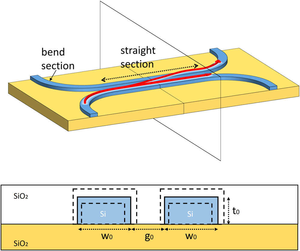
A DC consists of two parallel waveguides and connecting bend sections: the light in a single waveguide is mostly confined in the silicon core, but an exponentially decaying field extends into the cladding. When two waveguides are brought in proximity, the modes of the two waveguides couple and form two supermodes with opposite symmetry (an even and an odd mode). The beating of these supermodes translates in a sinusoidal power transfer from one waveguide to the next and back along the propagation axis . The power coupling in a DC can be expressed as [23]The power coupling consists of two parts: the contribution of the straight waveguide and of the bend section . The bend part will introduce an initial phase in the coupling term. Usually, the bend contribution is fairly small, and the power coupling is sinusoidally varying with the waveguide coupling section length .
The rate of coupling is defined as the field coupling coefficient , which is determined by the geometry of the coupler cross section, such as the waveguide width, thickness, and gap between the waveguide cores.
Let us assume that, for simplicity, the two waveguides in a DC are identical. As a result, the straight section of the DC layout is defined by three parameters: the waveguide width , thickness , and gap (Fig. 1). Furthermore, we assume that, in the lithography process, the centers of the two waveguides are located at the designed position. It is a good assumption for optical lithography techniques but might be less accurate for e-beam written devices. With this assumption, the sum of the gap and the half-waveguide width is constant, as shown in Fig. 1. Therefore, in our example, we can describe the full geometry of the DC with only two parameters: and .
Figure 1.Upper plot shows the perspective view of a symmetric DC. Red arrows present the flow of light. Part of the light is coupled from bottom waveguide to the above one. Cross section is amplified in the lower plot. The mean width and thickness of the DC are and , respectively. The width and thickness of the fabricated DC are indicated as dashed boxes. The refractive indexes are , .
In this study, we will use the SC technique to find out how geometry variability influences the DC performance, namely, the coupling coefficient . Indeed, due to the fabrication variations, the fabricated linewidth , thickness , and gap are different on the value chosen during the design phase. To prove the robustness and modeling power of the proposed approach, we assume the width and thickness of the DC as correlated random variables, rather than independent, following the Gaussian distribution. It is not an unrealistic assumption: thickness variations could induce over-etching on the sidewalls.
It is good to note that the SC methods can deal with random variables with arbitrary distribution. It is therefore not necessary that the and adhere to a Gaussian distribution.
B. Simulation Setup
According to the theory of supermodes, we can write the coupling coefficient as [23]where and are the effective index of asymmetrical and symmetrical supermodes in DC. For our silicon photonics devices, we assume the wavelength to . Next, the nominal value of the width and thickness are and , respectively, while we fix the sum of width and gap at 650 nm.
To calculate of a given geometry, we define the DC structure accordingly and simulate and in the mode solver Fimmwave using its film matching mode (FMM) solver. For later performance comparisons, all simulations are performed on a computer with an Intel Core i5 2500 quad-core CPU clocked at 3.3 GHz and 8 GB of memory.
C. Problem Definition
As mentioned in Section 3.A, we considered the coupling coefficient of a DC as a stochastic process depending on two correlated random variables with Gaussian PDFs: the width and thickness . Hence, the joint PDF of the two random variables considered is defined as where is the vector of the correlated random variables considered, the vector contains the corresponding nominal values (mean values) and , and the matrix is the covariance matrix. The symbol represents the matrix determinant operator. The covariance matrix is defined as where the symbols and are the normalized standard deviations of the and , while is the correlation coefficient of these two random variables. The correlation coefficient denotes the strength of correlation: the random variables considered are independent if and strongly correlated if . Note that, by describing this example in terms of normalized standard deviations, we make further analysis independent of the actual nominal values of our two random variables.
To validate the robustness of the proposed method, and are chosen equal to 2% and the correlation coefficient , which is a challenging example to study because the coupling coefficient is quite dynamic with respect to the parameters considered (see Fig. 2). The proposed method is discussed in detail in the following and summarized in Fig. 3.
Figure 2.2D contour plot of field coupling coefficient versus waveguide width and thickness.
Now, SC methods in the form of Eq. (1) deal with independent random variables, as described in Section 2. Hence, to fit the problem into the SC framework, first of all, it is necessary to express the coupling coefficient in two independent Gaussian random variables, starting from the correlated random variables , defined by Eq. (9). As mentioned in Section 2, such decorrelation can be obtained via a variable transformation. Thanks to the Karhunen–Loéve expansion [21], it is possible to express the vector of correlated Gaussian random variables in the vector of uncorrelated Gaussian random variables with zero mean and unit variance as where and are the diagonal matrix of the eigenvalues and the full matrix of the eigenvectors of the covariance matrix , respectively. Because uncorrelated Gaussian random variables are also independent, we have now expressed the coupling coefficient as a stochastic process, which depends on the pair of independent Gaussian random variables . An accurate description of the Karhunen–Loéve expansion for Gaussian random variables is given in Appendix 5.A.
E. SC Model Computation
To compute an SC in the form of Eq. (1), the first step is choosing the interpolation scheme: the Lagrange interpolation scheme is adopted in this example for its modeling power and ease of implementation. Next, a rule that guarantees a good quality of the approximation must be used to choose the collocation points for each random variable: and . In this example, the Clenshaw–Curtis rule is adopted [17]: the collocation points for each random variable are the extrema of the Chebyshev polynomials. Now, the total number of nodes could be obtained using the full tensor products of the nodes chosen for each random variable, but it would not be efficient, as discussed in Section 2. Instead, the nodes are chosen over a sparse grid based on the Smolyak algorithm. Indeed, the adoption of the Smolyak algorithm allows building our SC model by using only a subset of all the collocation points given by the full tensor product [17]. Furthermore, the collocation points chosen by the Smolyak algorithm based on the Clenshaw–Curtis rule are nested: if additional nodes are required to accurately model the DC, the nodes already computed are kept in the new sparse grid, thus reducing the number of evaluation of the DC coupling coefficient. (See Appendix 5.B for additional details on the Smolyak algorithm.) As a result, only 65 collocation points (Fig. 4) are required to build the desired SC model, and the values of the coupling coefficient at the interpolation nodes are computed using the FMM solver Fimmwave.
Figure 4.Top: the red exes represent the interpolation nodes for the normalized independent random variables and used to build the SC model. Bottom: the blue circles are the corresponding values for the correlated random variables and used to compute the coupling coefficients in Fimmwave.
Finally, the variability analysis for the coupling coefficient of the DC under study is performed using an SC model depending on the pair of independent Gaussian random variables and the results obtained are validated through comparison with an MC analysis based on the Fimmwave FMM solver on the DC cross section for the couple of correlated random variables . To compare the performance of the two methods, the same set of 10000 samples for the pair of correlated random variables (see Fig. 5). The corresponding values for the independent random variables are used to estimate the device variability features.
Figure 5.Sampling points used to perform the MC analysis through direct Fimmwave simulations for the correlated random variables . The corresponding values for the independent random variables are used to evaluate the SC model computed.
The proposed method shows an excellent accuracy compared with the classical MC analysis, as shown in Table 1, Figs. 6 and 7. In particular, the mean and the standard deviation of the coupling coefficient obtained employing the two methods are reported in Table 1: the relative error in the estimation of the mean and the standard deviation is only and , respectively. Apart from stochastic moments, more complicated functions of the stochastic process under study can be estimated: the probability density and cumulative distribution function (CDF) of obtained utilizing the two methods considered are in excellent agreement, as shown in Fig. 7.
MC
SC
Mean value
65,160
65,166
S.t.d value
2616.9
2631.4
Table 1. Performance Summary of SC and MC Simulation
Figure 6.Blue circles : coupling coefficient computed via the MC analysis for the 10000 samples shown in Fig. 5. Red -markers: corresponding values obtained by evaluating the SC model.
Figure 7.PDF and CDF of the coupling coefficient for . The blue solid and red dashed line are PDF and CDF obtained by means of the SC model, respectively, while the blue circles and red squares represent the same quantities computed by means of the MC analysis.
From the field coupling coefficient, we can also easily derive performance parameters of a DC such as 3 dB coupling length from As shown in Fig. 8, the proposed method shows excellent modeling accuracy and a good estimation of the PDF and the CDF of the 3 dB coupling length .
Figure 8.PDF and CDF of the 3 dB-coupling length for . The blue solid and red dashed line are PDF and CDF obtained by means of the SC model, respectively, while the blue circles and red squares represent the same quantities computed by means of the MC analysis.
Furthermore, as presented in Table 2, the SC method has dramatically saved computational cost. Note that the SC method took a two-step procedure to perform the same variability analysis. Initially, SC required 65 simulations to compute the coupling coefficient at the collocation points. Next, we used the SC model over 10000 samples of the independent random variables in the MC method. Hence, the total computational time of the SC method is 8 min and 59 s, which represents a speed-up of a factor with respect to the MC analysis performed in Fimmwave for the couple of correlated random variables , which required 21 h 53 min 14 s.
This paper has presented the application of a novel technique for the efficient variability analysis of photonic devices, such as DCs. It is based on the use of SC methods. Thanks to the flexibility in the choice of the interpolation schemes and the efficiency of sparse grid sampling to choose the collocation nodes for multiple dimension, the proposed approach is flexible and can be applied to study a broad range of photonic devices. The accuracy and efficiency of the proposed technique have been verified using comparison with the classic MC analysis for a pertinent numerical example, achieving a simulation speed-up of .
[3] L. Chrostowski, X. Wang, J. Flueckiger, Y. Wu, Y. Wang, S. T. Fard. Impact of fabrication non-uniformity on chip-scale silicon photonic integrated circuits. Optical Fiber Communication Conference, Th2A.37(2014).
[7] P. R. Johnston. Defibrillation thresholds: a generalised polynomial chaos study. Conference in Computing in Cardiology(2014).
[8] K.-K. K. Kim, R. D. Braatz. Generalized polynomial chaos expansion approaches to approximate stochastic receding horizon control with applications to probabilistic collision checking and avoidance. IEEE International Conference on Control Applications(2012).
[9] D. Cassano, F. Morichetti, A. Melloni. Statistical analysis of photonic integrated circuits via polynomial-chaos expansion. Advanced Photonics, JT3A.8(2013).
[11] M. S. Eldred. Recent advance in non-intrusive polynomial-chaos and stochastic collocation methods for uncertainty analysis and design. Proceedings of 50th AIAA/ASME/ASCE/AHS/ASC Structures, Structural Dynamics, and Materials Conference(2009).