
Yamei LIU, Haihang MA, Yan GU, Zhou HUANG, Shun ZHANG. Preparation of Double-sided Grating Structure Film by Vibration-assisted Nanoimprinting Lithography[J]. Acta Photonica Sinica, 2022, 51(6): 0631002
- Acta Photonica Sinica
- Vol. 51, Issue 6, 0631002 (2022)
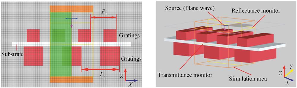
Fig. 1. Schematic of FDTD simulation model
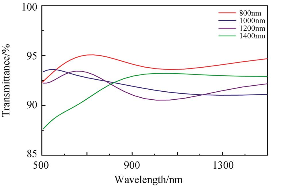
Fig. 2. Transmittance of upper surface gratings with different periods in the wavelength range of 500~1 500 nm
Fig. 3. Transmittance of lower surface gratings with different periods in the wavelength range of 500~1500 nm
Fig. 4. Mathematical model of vibration-assisted nanoimprint mechanism
Fig. 5. Influence of vibration frequency on filling rate of the upper surface
Fig. 6. Influence of vibration amplitude on filling rate of the upper surface
Fig. 7. Influence of vibration amplitude on filling rate of lower surface
Fig. 8. Flow chart of vibration-assisted nanoimprinting experiment
Fig. 9. Vibration-assisted nanoimprinting device
Fig. 10. SEM inspection image of grating structure
Fig. 11. SEM inspection image of grating structure prepared by traditional nanoimprint
Fig. 12. The transmittance test diagram of SiO2 without film and SiO2 with double-sided grating structure film prepared by vibration-assisted nanoimprinting and conventional nanoimprinting
|
Table 1. Correspondence between the period parameters of the upper surface gratings and the average transmittance
|
Table 2. Correspondence between the period parameters of the lower surface gratings and the average transmittance

Set citation alerts for the article
Please enter your email address
© Copyright 2018-2021 | Chinese Laser Press. All Rights Reserved 沪ICP备15018463号-20