Muhammad Saeed, Izaz Ul Haq, Shafiq Ur Rehman, Akbar Ali, Wajid Ali Shah, Zahid Ali, Qasim Khan, Imad Khan. Optoelectronic and elastic properties of metal halides double perovskites Cs2InBiX6 (X = F, Cl, Br, I)[J]. Chinese Optics Letters, 2021, 19(3): 030004
Copy Citation Text
Structural geometry, electronic band gaps, density of states, optical and mechanical properties of double perovskite halides (X = F, Cl, Br, I) are investigated using the density functional theory. These compounds possess genuine perovskite stoichiometry, evaluated using various geometry-based indices like tolerance factor, octahedral factor, and formation energy. The fundamental electronic band gaps are direct and valued in the range 0.80–2.79 eV. These compounds have narrow band gaps (except ) due to strong orbital coupling of the cations. The valence band maximum and conduction band minimum are confirmed to be essentially of In 5s and Bi 6p characters, respectively. The splitting of Bi 6p bands due to strong spin-orbit coupling causes reduction in the band gaps. These compounds have large dispersion in their bands and very low carrier effective masses. The substitution of halogen atoms has great influence on the optical properties. The mechanical properties reveal that (X = F, Cl, Br, I) satisfy the stability criteria in cubic structures.
The appearance of lead (Pb) tri-halide perovskites in photovoltaic cells resulted in power conversion efficiency up to 25.2% in 2020[1,2], which offers an extraordinary prospect for wider use of solar energy. Pb halide perovskites have exceptional properties such as high charge carrier mobilites, direct and tunable band gaps, small effective masses of electrons and holes, high absorption, balanced electron and hole transport, and long carrier diffusion length[3–9]. Due to the remarkable structural, electrical, optical, electronic, magnetic, catalytic, and superconducting properties, halide perovskites find many applications in new areas of technology[10–14]. They are widely used as optical functional materials in different devices like light emitting diodes (LEDs), solar cell absorbers, X-ray detectors, lasers, batteries, photodetectors, and quantum dots[15–20]. Extensive research has been carried out on photovoltaic hybrid organic–inorganic perovskites () using Pb as a B-site cation from the last 10 years[21–23]. However, Pb perovskites undergo intrinsic structure instability when exposed to moisture, light, air, and high temperatures. In addition, Pb is a most toxic element and compounds containing high content of Pb are reported harmful to health and the environment[24,25].
Overcoming this toxicity and instability problem gives rise to research work committed to investigating Pb free perovskites free of intrinsic structure instability and poverty under external stimuli[24,26]. It is highly desirable to identify Pb free materials that have properties of the extensively studied perovskites[3]. The effective replacement of Pb from perovskite halides leads us to adopt different structural designs. Pb can be replaced by other group IV elements, e.g., Ge and Sn, as and , but their use provides chemical instability due to the preferred poor oxidation state and poor optoelectronic performance[27]. Inorganic perovskites (, Cl, Br, and I) are more thermally stable in contrast to organic–inorganic hybrid perovskites[28–30]. Alternatively, two Pb can be replaced by a pair of monovalent and trivalent ions leading to the structure of organic/inorganic double perovskites having the general formula (, , , )[18]. The crystal structure of double perovskite is stable and the same as in most oxides. Moreover, introducing different metal cations on site B, diverse organic and inorganic cations on site A, and a variation of halide compositions on site X can fabricate highly efficient materials comparable to () and [26,31]. Double perovskite halides are emerging efficient materials in numerous applications such as ferroelectrics, electrocatalysts, phosphors, white light emitters, spintronics, magnetoresistive materials, and solar absorbers[32,33]. The early synthesized organic double perovskite methyl ammonium and formamidinium are not stable and not suitable for the use of photovoltaic cells[34–38]. Small amounts of inorganic cations like doping with methylammonium and formamidinium at the A site can raise the stability of perovskites[29,39–42]. Inorganic double perovskite halides (with , Bi; , Cu, Au, and , Br, I) are useful for optoelectronic purposes when their band gaps lie in the visible range of the electromagnetic spectrum[43]. The successful candidates for solar cells are and . These compounds are more stable and absorb light in the visible range of the electromagnetic spectrum. The structures of these compounds are highly symmetric faces of center cubic double perovskites. and are indirect band gap semiconductors, and is s synthetically stable and non-harmful perovskite having a band gap of 2.19 eV by diffuse reflectance spectroscopy and 1.95 eV by photoluminescence[44,45]. It has limited applications in photo cells because of its low absorption of light[46].
In metal halides perovskites, the A-site cation is not involved in the formation of the frontier band edges; on the other hand, anions at the X site (F, Cl, Br, I) modulate the size [in electron volts (eV)] of the band gap but have nothing with the orbital character and direct/indirect nature of the band gap[47]. Therefore, the efficiency of metal halide perovskites in solar cells and LEDs can be tuned by smart choices of and sites cations. Choices for the site are (i) elements of group III (In, Tl), (ii) pnictogens, and (iii) several transition metals (Cr, Mn). For the site, the possible candidates are (i) noble transition metals (Ag, Au), (ii) lanthanides, (iii) some actinides (Pu, Am, and Bk), (iv) elements of group III (In, Tl), and (v) alkaline metals (Na, K). Among these, lanthanides, actinides, and transition metals have partially or orbitals, so they would have band extremes of such states. Group III elements in the oxidation state have the highest occupied states of the character at the top of the valence band. The pnictogens such as and are not stable in perovskite structures because of their small size, according to Goldschmidt’s rule. Arsenic is toxic, and the possible candidates to realize double perovskites from the pnictogen family are and .
Sign up for Chinese Optics Letters TOC. Get the latest issue of Chinese Optics Letters delivered right to you!Sign up now
Potential contestants for the site in double perovskite halides are alkaline metals, elements of group III, and noble transition metals. Out of these three, alkaline metals give non-dispersive bands and hence are not suitable for photovoltaic perspectives. Cations of the noble transition metals occupy the highest orbital of the character when it is in the oxidation state. This situation will lead to valence band maximum of the character and is not needed[26]. Group III elements have filled and orbitals when they are in the oxidation state; in this configuration, electrons are deeper than electrons. The suitable elements from group III are In and Tl (the rest have low atomic numbers and cannot exist in the oxidation state); as Tl is toxic, the sole option for us is In [48].
Zhao et al.[49] proposed that -based double perovskites and are useful solar cell absorbers because their band gaps are direct, having band gaps of 1.02 eV and 0.91 eV, respectively. These predictions were provided by the relatively new hybrid functional, including spin-orbit coupling (SOC) [Heyd–Scuseria–Ernzerhof (HSE + SOC)] calculations. These two perovskites are found to be thermodynamically stable against decomposition with small effective masses of electrons and holes[50]. The oxidation state is rare; however, InCl and are the compounds in which the oxidation state has been reported[51,52]. Although theoretical studies proposed that and (X = Cl, Br, I) have admirable optoelectronic properties including direct band gaps and small carrier effective masses, they are unstable due to the favorable oxidation state of In [53]. To the best of our knowledge, successful synthesis of these double perovskites has not been reported. The replacement of the A-site cation in these compounds with a large sized mixed cation such as can passivate the oxidation process and might solve the stability problem[26,32,47]. Substitution of the A-site cations can provide stability to double perovskites[29,39–42], but have no contribution in the formation of frontier bands and therefore have negligible effects on the optoelectronic properties[2,47]. These compounds have been studied theoretically, yet there is a lack of literature about their elastic and optoelectronic nature. In this article, an attempt has been made to study the stability and effect of anion substitution on the structural, chemical bonding, electronic, elastic, and optical properties of (X = F, Cl, Br, I) using different exchange-correlation approximations of the density functional theory (DFT). These compounds are direct band materials in contrast to other inorganic double perovskites. The calculated band gap of is 1.37 eV, close to the optimal band gap (1.4 eV) for photovoltaic applications. The absorption edge of these compounds is found to be similar to the best-identified material () for solar cells. The present work will not only to help us understand the optoelectronic and mechanical properties of (X = F, Cl, Br , I), but will also motivate researchers to explore double perovskite halides for practical applications.
2. Details of Calculations
DFT is used to calculate the structural, electronic, optical, and elastic properties of Pb free inorganic double perovskite halides (X = F, Cl, Br , I). The calculations are done using the full potential linearized augmented plane wave (FP-LAPW) method implemented in the Wein2k package[54]. Exchange-correlation energy is dealt by generalized gradient approximation (GGA) Perdew–Burke–Ernzerhof for solids (PBEsol)[55], because it is more effective compared to other GGA characteristics for the calculation of structure optimization[56]. For the calculations of electronic properties of GGA, modified Becke–Johnson (mBJ) and mBJ with SOC () are used. GGA often gives much underestimated results as compared to experiments[57,58]. The mBJ[59,60] exchange potential in addition to GGA is known for its remarkable success in reproducing experimental band gaps of semiconductors in general and halide perovskites in particular[60]. These compounds contain heavy elements like Bi; therefore, SOC calculations have been carried out for better treatment of different orbital splitting in electronic and optical properties. Self-consistent calculations throughout the Brillouin zone were carried out using 2 × 10⁶ points.
3. Results and Discussion
3.1. Structural Properties
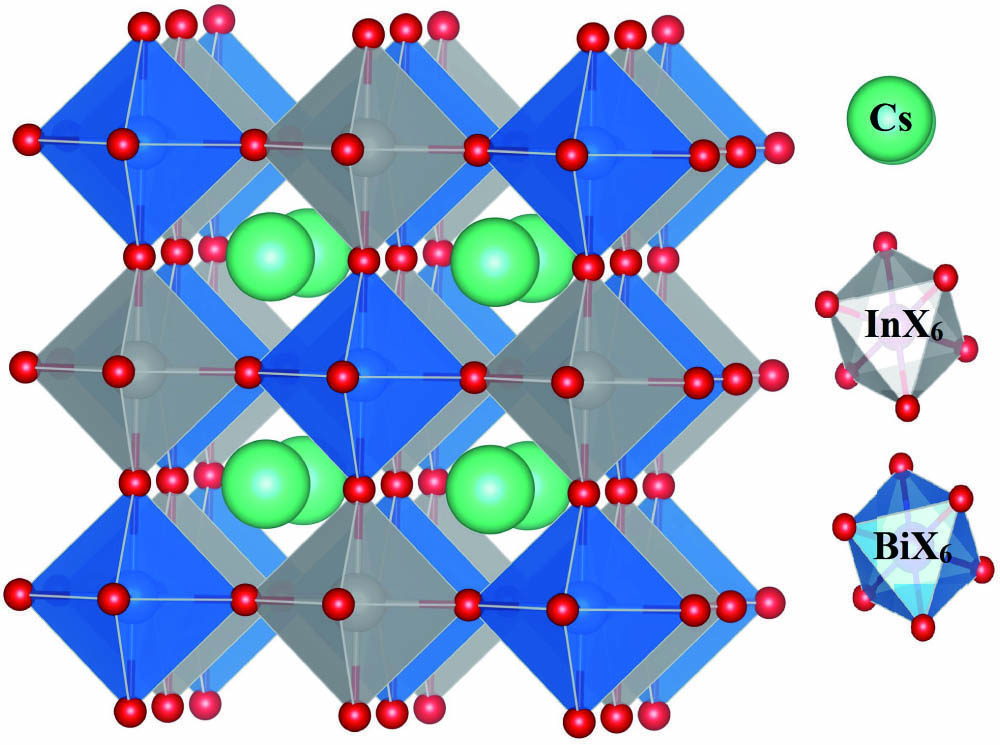
The crystal structure of is cubic and belongs to space group Fm-3m (225)[49]. The unit cell structure of (X = F, Cl, Br, and I) shown in Fig. 1 possesses 10 atoms. The figure illustrates that, like the basic perovskite structure (), double perovskite is a three-dimensional (3D) framework, in which the A cation (here ) occupies the cubic octahedral cavity formed by corner shearing of In and Bi octahedra. These octrahedra have fascinating roles in the physical properties of perovskites.
Figure 1.Unit cell structure of (X = F, Cl, Br, and I).
In order to get ground state energies, unit cells of (X = F, Cl, Br, and I) are optimized using the reported[49] lattice parameters, symmetry of the space group, and atomic coordinates. Total energy versus volume curves are plotted in Fig. 2 for compounds, and the obtained values are then fitted to Birch Murnaghan’s equation of states[61]. The calculated lattice constants are listed in Table 1. Halogen replacement caused a systematic increase in the lattice constant; this increase is due to the increase in size of anions from F to I.
Parameters
X = F
X = Cl
X = Br
X = I
a (Å)
9.70
11.07
11.30
12.32
9.80a
11.44a
11.93a
12.69a
τ
Eq. (1)
0.95
0.90
0.89
0.87
Eq. (3)
3.49
4.01
4.07
4.13
μ
0.68
0.53
0.47
0.44
rij (Å)
Bi–X (x6)
2.25
2.73
2.79
2.82
In–X (x6)
2.60
3.00
3.09
3.15
Cs–X (x12)
3.43
4.06
4.12
4.20
Eg (eV)
GGA
2.01
0.38
0.25
0.12
mBJ
2.79
1.37
0.82
0.80
mBJ + SOC
1.87
0.87
0.32
0.23
HSE + SOC
2.22a
1.02a, 0.88b
0a, 0.33b
0a, 0.21b
me*
mBJ
0.73
0.52
0.37
0.28
mBJ + SOC
0.58
0.38
0.29
0.24
HSE + SOC
0.61a
0.39a
0.30a
0.23a
MaPbI3
0.19c
mh*
mBJ
0.46
0.23
0.19
0.13
mBJ + SOC
0.37
0.19
0.14
0.09
HSE + SOC
0.39a
0.17a
0.11a
0.08a
MaPbI3
0.25c
Table 1. Calculated Tolerance Factor τ, Octahedral Factor μ, Lattice Constants a, Bond Lengths rij, Band Gap Eg, and Effective Masses of Electrons and Holes (mo) of Cs2InBiX6
For structure stability of these double perovskites (X = F, Cl, Br, I), a modified tolerance () factor and an octahedral factor () are calculated from the ionic radii of the different components given in the formulas[63]where is the average radius of and ; and are the radii of Cs and halogen atoms. The calculated values of tolerance and octahedral factors are listed and compared with other theoretical results in Table 1. A value in the range of and a value in the range of have been suggested, X atoms in the (100)[49]. The tolerance factor varies between 0.95 and 0.87, and the octahedral factor lies in the range of 0.68 to 0.44; the tolerance and octahedral factors reveal that (X = F, Cl, Br, I) adopts an ideal perovskite structure. The accurate and probabilistic nature of the tolerance factor as well as its applicability over a broad range of perovskites creates a new physical insight into the stability and the prediction of new stable organic, inorganic, and hybrid perovskites. A new tolerance factor formula is used for perovskite structure stability[32]:where is the oxidation state of the A atom. The calculated values of using Eq. (3) are listed in Table 1, which clarifies that the values are below 4.18 (stable perovskites are expected when )[32]. The tolerance and octahedral factors confirm the stability of in cubic crystal structures, and, hence, these compounds are investigated in elpasolite structures with space group Fm-3m, which corresponds to an ideal double perovskite.
Formation energies of (X = F, Cl, Br, I) compounds have been calculated in order to determine their stability[64,65]:where is the ground state energy of a single atom, is the number of atoms of that species, and represents the total number of atoms in a unit cell. The energy of a single atom can be calculated by optimizing an isolated atom. The calculated formation energies of , , , and are , , , and −15.12 eV, respectively. The negative formation energies confirm the thermodynamic stability of these compounds.
3.2. Chemical Bonding
For studying bonding aspects of these materials, we examine the electron charge densities of the understudy compounds. The electron charge densities for crystal planes (100) and (110) are plotted in Fig. 3. The overlapping counters between Bi and X atoms in the (100) plane reveal a covalent bond and correspond to octahedra. In plane (110), the counters In and X overlap each other, which confirm covalent bonds and correspond to octahedra. The non-overlapping and spherical symmetric counters of Cs show ionic bonds between Cs and X. The calculated bond lengths are listed in Table 1. The table reveals that the bond lengths increase from Cl to I, and this increase is related to the decreasing electronegativity and increasing size of the halogens. The electronegativities of Cs, In, Bi, F, Cl, Br, and I are 0.79, 1.78, 2.02, 3.98, 3.16, 2.96, and 2.66, respectively, on a puling scale basis.
Figure 3.Electronic charge density contours in the [100,110] planes.
In order to examine the electronic nature, the band structure and density of states (DOS) are used to look at whether materials are insulators, conductors, or semiconductors. The band structure and DOS calculations are performed using GGA, mBJ, and mBJ + SOC. Figure 4 reveals that (X = F, Cl, Br, I) is direct band gap materials. The valence band maximum (VBM) and conduction band minimum (CBM) both lie on the same Γ symmetry line of the Brillouin zone. Direct band gap materials are more efficient for optoelectronic applications as compared to indirect band gap because of phonon involvement, which make indirect band gap semiconductors bad emitters of light[57,58]. Zhao et al.[49] and Xiao et al.[53] also reported direct band gaps of (X = F, Cl, Br, I) using the method. Figure 4 shows that SOC pushed the valence and conduction bands toward the Fermi level that caused reduction of the band gaps in these compounds. SOC splits the Bi 6p in the conduction band, pushing one of the orbitals toward the Fermi level and reducing the band gap. The band gap values are listed in Table 1. GGA underestimates band gaps of (X = F, Cl, Br, I). Our results calculated with are consistent with the reported data[49,53]. MBJ is renowned for its excellent band gap production near the experimental values. The calculated band gap value of is closer (the best solar cell material has a band gap of 1.55 eV) to the optimal value for photovoltaic performance (1.4 eV)[66].
Figure 4.Electronic band structures of (X = F, Cl, Br, I).
DOS is mostly used for physical properties of materials like dielectric spectra, photoemission spectra, and transport properties. It shows the role and location of different energy orbitals in the formation of a band structure. Total DOS and partial DOS of , , , and compounds are given in Figs. 5 and 6, respectively. The Fermi level separates the valence and conduction bands. From the total DOS, it is clear that SOC pushes the conduction band towards the Fermi level, which reduces band gaps of these metal halides. The partial DOS demonstrates that In 5s contributes to VBM. The halogen p orbitals have a dominant role in the formation of bands in the energy range of −2 to −4 eV in the valence band. Bi 6p orbitals have contributed bands at energy of −4.5 eV in the valence band.
Figure 6.Partial density of states of (X = F, Cl, Br, I).
The CBM is derived primarily from the Bi 6p orbitals, whereas In 5p orbitals have significant contributions in the energy range from 4 to 6 eV in the conduction band. The small band gaps of compared to other metal halide perovskites are due to the fact that strong sp coupling between the 5s state of In and orbitals of halogen endorses the VBM to relatively high energy with respect to the CBM[67]. Figure 6 also reveals that SOC splits Bi 6p orbitals in the conduction bands and pushes one of the Bi 6p orbitals towards the Fermi level, which further reduces the band gap of these compounds. The high energy In states, which occupy VBM, are mainly responsible for the promising photovoltaic properties of (X = Cl, Br, I)[53]. Such high energy states at the top of the valence band are stable with respect to decomposition[49].
Band dispersion and carrier effective masses play a vital role in the efficiency of solar cells and other optoelectronic materials. The VBM and the CBM of (X = F, Cl, Br, I) are located at Γ symmetry of the Brillouin zone and have large band dispersion. This large band dispersion results in the small carrier effective masses[49]. The effective masses of electrons and holes are calculated from the parabolic fitting of the band edges according to the relationwhere and represent band edge eigen values and wave vectors, respectively. The effective masses of electrons and holes are listed and compared with the reported data in Table 1. The table reveals that has quit small carrier effective masses. Our calculated values of the carrier effective masses are in good agreement with the reported work[48]. The effective masses are also compared with . It is evident from the table that SOC not only splits the band but also alters the values of the carrier effective masses.
3.4. Optical Properties
The interaction of light with the material medium is expressed in terms of optical properties. Presently, we study optical properties of metal halide double perovskites (X = F, Cl, Br, I) under the DFT scheme by measuring their different optical parameters.
The study of polarization and absorption of electromagnetic radiation within the material medium is expressed in dielectric functions, which are mathematically presented by a relation . In this relation, the first term represents the real part , which shows polarization of light, while the second term represents imaginary part of the dielectric function, which measures the extent of light absorption. The calculated zero frequency limits (static dielectric constant) are listed and compared in Table 2. This reveals that increases as the band gap decreases from F to I, meaning that band gap energy has an inverse relation to , which is consistent with the Penn model[68]. These compounds have remarkable large values of comparable with that of and . The maximum value of is observed in the visible energy range (2–2.5 eV) and then rapidly decreases, and small humps are observed, which can be related to interband transitions between valence and conduction bands. has a dielectric constant of 6.5 in the visible spectral range at the temperature of 4.2 K[71]. The understudy compounds have larger values of dielectric function than in the visible spectral region.
Compounds
ε1(0)
n(0)
Cs2InBiF6
2.73
1.66
Cs2InBiCl6
4.65
2.10
Cs2InBiBr6
6.00
2.47
Cs2InBiI6
6.10
2.49
CsPbI3
5.00a
2.1a
MAPbI3
6.00b
1.68b
Table 2. The Zero-Frequency Values of the Real Part of the Dielectric Function and Refractive Index
The imaginary part of the dielectric function is the measure of the extent of light absorption. It is a seed parameter and can be directly calculated from the Fermi–Golden rule; all other optical parameters including are calculated from . The first onsets of absorption (absorption edge) are observed roughly at 2.75, 1.35, 0.80, and 0.80 eV for , , , and , respectively. These onsets are close to the fundamental band gaps of these compounds. The absorption edge of is very close to that of , which is found at ∼1.55 eV[71]. Halogen substitution significantly changes the positional occurrence of the transition peaks. High absorption peaks are observed in the visible spectral region at energy around 2–3 eV. Several weak peaks are observed in the energy range of 3–15 eV.
Knowledge of the refractive index is necessary for the effective use of a material in photonic and optical devices. Refractive indices are inversely proportional to the band gap of a material, i.e., wide band gap materials have small values of refractive indices and vice versa. The refractive indices for compounds are shown in Fig. 7. The zero frequency limit of refractive index values are listed in Table 2. The maximum peaks of the index of refraction for , , and are observed in the energy range of 2–2.5 eV for these compounds. The peak values are larger than the refractive index of (2.61) in the visible spectral range[71]. Appreciable values of below 4.5 eV suggest that is opaque against light. It explores interactions of the incident photons and explains various features of a semiconductor. The calculated for is plotted in Fig. 7, in which no scattering happens when the energy of the photon is less than the band gap energy. The highest peaks appear at the energy range of 17–20 eV. These peaks show plasma resonance, and their frequencies are called plasma frequencies.
The mechanical properties of a material play an important role in structure stability and strength of a material to an exterior force, and are associated with basic phenomena of solid state, like inter-atomic bonding, phonon spectra, and equation of state. Mechanical properties are computed using independent elastic coefficients calculated using the Charpin package embedded in Wien2k and listed in Table 3.
Parameters
X = F
X = Cl
X = Br
X = I
C11 (GPa)
98
81
105
71
C12 (GPa)
35
28
31
20
C44 (GPa)
57
44
41
62
GV (GPa)
46.8
37.0
39.4
47.4
GR (GPa)
43.0
34.8
39.3
39.4
GH (GPa)
44.9
35.9
39.3
43.4
Y (GPa)
103.2
87.3
95.6
99.6
B (GPa)
49.2
45.6
55.6
37.0
B/G
1.09
1.27
1.41
0.85
C″
−22
−16
−10
−42
ν
0.15
0.18
0.21
0.05
Z
0.61
0.59
0.52
0.50
A
1.80
1.66
1.100
2.43
C′
31.5
26.5
37.00
25.5
λ
19.1
21
29.4
5.4
μ
60.7
37
39.4
47.4
Table 3. Calculated Values of Elastic Constants Cij, Shear Modulus G, Young's Modulus Y, Bulk Modulus B, Shear Constant C′, Cauchy Pressure C″, B/G Ratio, ν, ζ, A, λ, and µ Parameters
The calculated results satisfy the Born mechanical stability criteria, i.e., , , and [72], which show that these compounds are a mechanically stable perovskite structure. Resistance of a material to reversible deformation upon shear stress is calculated from shear modulus (G), which gives information about the rigidity of a material; thus, G is calculated using two models Voigt ()[73] and Reuss ()[74]:
However, Hill[75] () calculated the arithmetic mean of and :
The calculated values of show that has the highest value (43.3 GPa) of shear modulus, which clarifies that it is stiffer than the rest of the materials. The reaction of a material to linear deformation can be determined from Young’s modulus (Y), i.e., the toughness of a material depends on the value of Y. The higher the value of Y, the greater the toughness of a material will be, which is calculated using the relation
The larger value of Y (103.2 GPa) for indicates a high toughness among these compounds. Pugh’s ratio (B/G) can be used to examine the ductile/brittle nature of a material[76]; material is ductile if the value of B/G is less than 1.75, otherwise it represents a brittle nature. Pettifog and Chen have established the brittle versus ductile transition in different materials using first principles calculations[77,78]. Our calculated results show that these compounds have lesser value of B/G than the critical value of 1.75, which confirm that these materials are brittle in nature. The bonding nature of a material can be explained with the help of Cauchy pressure[78]. The value of Cauchy pressure is determined using the following equation:
Lower values of Cauchy pressure show directional response in bonding (covalent bonding), while higher values of Cauchy pressure result in ionic bonding. The values of mentioned in Table 3 confirm that these compounds are brittle in nature. The compressibility is measured with the help of Poisson’s ratio ν, which is the ratio of adjacent longitudinal strain in non-axial tensile stress:
A material having is considered incompressible[79], and has the tendency of compressibility, i.e., stretching a sample causes no adjacent reduction, so its volume remains the same no matter how distorted it is. The values of Poisson’s ratio for compounds (X = F, Cl, Br, I) lie in the range of 0.05–0.21, which show that these materials are incompressible.
The anisotropic parameter (A) of a material is given as
For an ideal isotropic system, the value of A is unity and diverges from unity for anisotropic systems. The calculated values are 1.80, 1.66, 1.100, and 2.43 for , , , and , respectively, which show the anisotropic nature of these materials. Shear constant () is another significant parameter, which explains the stability of a material:
The stability of a material requires , so the calculated positive values of C show that these compounds are elastically stable. The interior straining of a compound can be examined by a parameter called the Kleinman parameter ()[80]. It explains the bond stretching versus bond bending given asThe zero value of ζ indicates minimization of bond bending, while ζ = 1 indicates minimization of bond stretching. The tabulated values confirm bond stretching in these compounds. Another motivating mechanical parameter is Lame’s constants (λ, μ), which are used to define anisotropy of a material:
For isotropic materials, and . The calculated Lame’s coefficients of (X = F, Cl, Br, I) are given in Table 3, confirming the results obtained from the anisotropic parameter (A) and showing that these materials are anisotropic.
4. Conclusions
It is summarized that the understudy compounds (X = F, Cl, Br and I) are theoretically investigated in the framework of the DFT. Goldschmidt’s tolerance factor, octahedral factor, the newly proposed tolerance factor, formation energy, and elastic constant demonstrate that these compounds possess a stable perovskite structure. The mechanical parameters reveal that these compounds are brittle and anisotropic. These perovskites are optically active materials in the infrared spectral region. The substitution of the anion tuned the band gap from 2.79 to 0.80 eV. The valence band is dominated by In and X orbitals, where the conduction band is mostly made of Bi states. High dielectric materials comparable to are found, and interesting variations are observed in their optical properties.
[3] M. Ghasemi, M. Hao, M. Xiao, P. Chen, D. He, Y. Zhang, W. Chen, J. Fan, J. H. Yun, B. Jia, X. Wen. Lead-free metal-halide double perovskites: from optoelectronic properties to applications. Nanophotonics(2020).
[72] M. Born. On the Stability of Crystal Lattices(1940).
[73] W. Voigt. Lehrbuch der Kristallphysik(1928).
[74] A. Reuss, Z. Angew. Berechnung der Fließgrenze von Mischkristallen auf Grund der Plastizitätsbedingung für Einkristalle. Math. Mech., 9, 49(1929).
Muhammad Saeed, Izaz Ul Haq, Shafiq Ur Rehman, Akbar Ali, Wajid Ali Shah, Zahid Ali, Qasim Khan, Imad Khan. Optoelectronic and elastic properties of metal halides double perovskites Cs2InBiX6 (X = F, Cl, Br, I)[J]. Chinese Optics Letters, 2021, 19(3): 030004