
Shunfa Gong, Ruirui Wu, Sen Yang, Lifang Wu, Minmin Zhang, Qiuju Han, Wenzhi Wu. Tuning the luminous properties and optical thermometry of Cs2SnCl6 phosphor microcrystals via Bi and Sb codoping[J]. Photonics Research, 2021, 9(11): 2182
- Photonics Research
- Vol. 9, Issue 11, 2182 (2021)
Abstract
1. INTRODUCTION
In recent years, organic-inorganic, and the subsequent all-inorganic lead halide perovskites [, , , or , , , or ] have attracted the attention of many researchers because of their unique optical properties, such as narrow full width at half-maximum (FWHM), high photoluminescence quantum yield (PLQY), wide color gamut, tunable emission, and excellent optoelectronic properties [1,2]. Therefore, researchers make use of the excellent optoelectronic properties of lead halide perovskite to prepare a large-area perovskite battery [3,4]. Taking advantage of the excellent optical gain and high emission efficiency of lead halide perovskite, high-quality nanowire plasmonic lasers have been fabricated successfully by chemical vapor deposition [5]. By making use of the tunable emission of lead halide perovskite, perovskite LEDs are prepared successfully [6,7]. However, the toxicity of lead will cause irreversible damage to human intelligence, especially for the brains of young children. Meanwhile, lead halide perovskite shows poor stability to oxygen, water, or high temperature, which seriously limits its commercial application prospects.
To solve the toxicity of lead and improve the stability of lead halide perovskite, researchers actively explore efficient substituted ways to change this situation. Recently, some research groups have turned to covalent elements to replace lead elements to solve the toxicity of lead halide perovskites, such as [8] and [9]. Nevertheless, these elements are easily oxidized for the high-energy-lying 5s orbitals, which leads to the perovskite being extremely unstable in the ambient atmosphere [10], and this kind of replacement will be affected by its low PLQY or poor stability. On the other hand, in addition to replacing lead with a single element, some research groups proposed to use another effective replacement method for lead-free perovskite. The problem of lead toxicity can be solved by combining (, , or ) and (, , or ) to replace double [11]. At the same time, this double perovskite structure also shows good stability to the natural environment, even exposed to oxygen or water vapor at high temperature. The double perovskite structure of completely avoids the toxicity of lead, and it also shows good environmental stability. Another effective solution is to directly replace double with single to form a lead-free defect perovskite variant. Although shows good thermal stability, its PLQY is very low. The main difficulty to improve application prospects is how to strengthen the PLQY. Bi-doped microcrystals (MCs) were successfully obtained by Tang
In this work, the steady-state PL and absorption spectra of bismuth (Bi) and antimony (Sb) codoped (BSCSC) MCs are measured at room temperature. Then the temperature-dependent steady-state PL and time-resolved PL (TRPL) are used to explore the luminous mechanism of BSCSC MCs. It is concluded that the peak position at 485 nm in the dual emission is attributed to the [] defect complex, and the emission of 650 nm is attributed to microsecond-timescale self-trapped excitons (STEs). Under 405 nm laser excitation, the fluorescence lifetime of BSCSC MCs is measured in the temperature range from 290 to 390 K. The maximum values of relative and absolute sensitivities are at 345 K and at 305 K. The dual emission of BSCSC MCs is applied in fabricating white-light-emitting diodes (WLEDs), avoiding the use of commercial light-emitting phosphors to reduce costs.
Sign up for Photonics Research TOC. Get the latest issue of Photonics Research delivered right to you!Sign up now
2. EXPERIMENTAL SECTION
A. Materials and Chemicals
The materials used are cesium chloride (CsCl, 99.9%, Aladdin), bismuth chloride (, AR, Aladdin), antimony trichloride (, AR, 99%, Macklin), tin chloride (, 99%, Macklin), hydrochloric acid (HCl, AR, 37% mass fraction, Harbin Polytechnic Chem. Reag. Co., Ltd.), and isopropyl alcohol (, AR, 99.5%, Macklin). All of these chemicals are used without any further purification.
B. Synthesis of BSCSC MCs
The BSCSC MCs are synthesized with the solvothermal method [16]. 5 mmol , 0.32–0.55 mmol , 0.32–0.55 mmol , and 10 mmol CsCl are dissolved in 10 mL HCl solution. A 50 mL Teflon autoclave filled with solution is heated at 180°C for 12 h. Then it is gradually cooled down to room temperature, and the cooling process is important in determining the PLQY [17]. After that, the upper solution from the precipitation in the whole sample is centrifuged and washed with isopropyl alcohol three times to separate impurities at 4000 r/min. The precipitation from the supernatant is collected via the same centrifugation method as described above. The obtained precipitate by centrifugation is dried in a vacuum oven at 60°C.
C. Fabrication of LED Devices
A UV-LED chip (380–390 nm) is used to fabricate the WLED and excite the phosphor-silicone mixture. The mixture contains BSCSC MCs phosphor and silicone gel A and B. First, phosphor is mixed with silicone gel A and B (A/B = 1/4). Then the bubbles in the silicone are removed through the vacuum chamber and overcoat the mixture on the chip. Finally, the chip is dried at 50°C for 2 h.
D. Steady-State PL and TRPL Measurements of BSCSC MCs
The 405 nm continuous-wave (CW) laser (FN-405-200mW, CNI) is used as an excitation light source for steady-state excitation. The steady-state PL spectra are collected by a spectrometer (HR4000CG-UV-NIR, Ocean Optics). The TRPL spectra are excited by frequency-adjustable picosecond laser (MDL-PS-405, CNI) pulses at 405 nm and collected by a spectrometer (SP-2500, Princeton Instruments) with an intensified CCD detector (PI-Max-1024i, Princeton Instruments). The temperature-dependent PL measurements are performed using a vacuum liquid-nitrogen cryostat (Cryo-77, Oriental Koji) with the capability to give a temperature range from 80 to 480 K.
3. RESULTS AND DISCUSSION
A. Basic Structural and Optical Characterization
In poor and rich conditions, the formation enthalpies () [12] obtained from the theoretical calculations are low and even negative, which makes Bi-on-Sn and Sb-on-Sn substitution possible. For a series of BSCSC MCs, Bi and Sb are codoped into the sample, and the and feeding ratios in the solution are set at 6% and 10% (6%10%BSCSC MCs). The others are named as 9%10%BSCSC, 12%10%BSCSC, 9%5%BSCSC, and 9%20%BSCSC MCs, respectively. The WLEDs reported in the previous paper [13] need to mix with other luminous powders. By codoping Bi and Sb into at the same time, WLEDs can be obtained directly without the addition of other light-emitting powders by applying them on the light-emitting chip. is doped with Bi only, and the peak is found to be at 454 nm [12]. The is doped with Sb, and the peak is located at 630 nm [18]. The dual emission peaks of 12%10%BSCSC MCs are at 485 and 650 nm under 405 nm CW laser excitation, and the intensity at this proportion is similar. The reason for the 20–30 nm redshift on the emission might be the expansion of Bi-anion and Sb-anion bonds [19].
From the left of Fig. 1(a), the crystal structure of BSCSC MCs shows a vacancy-ordered double perovskite structure with isolated octahedra [20]. The powders are white in the daylight, which with different elements or contents show different colors under the UV lamp (365 nm) as shown in the right of Fig. 1(a). Through controlling the Bi and Sb feeding contents, the emission of BSCSC MCs can be tuned, even to white-light emission. As shown in Fig. 1(b), whether Bi- (or Sb-)doped and 12%10%BSCSC MCs, each diffraction peak of all samples has a perfect match for the crystal structure (JCPDF#70-2413), which has an space group, and almost no impurity phase can be detected. It is noted that the diffraction peak (111) shows a fairly small peak shift as shown in the right side of Fig. 2(b). Compared with MCs, the X-ray diffraction (XRD) peaks of doped MCs have a slight peak shift, which can be proved that and are successfully doped into MCs. As shown in Fig. 1(c), the sharp optical absorption edge of at 320 nm is very close to the previously reported paper that showed excitonic absorption at 317 nm [21]. There is another absorption edge found at for Bi, Sb, and Bi-and-Sb-doped MCs. The absorption spectra show that only the doped samples have additional absorption peaks between 350 and 400 nm. The corresponding bandgap is calculated through the Tauc plot and labeled in Fig. 1(c). It can be seen that the bandgap of samples doped with Bi (or Sb) is smaller than that of undoped samples. The bandgap of 12%10%BSCSC MCs is the smallest in all samples due to the formation of the defect bands [12]. As shown in Fig. 1(d), the characteristic peak positions of every element can be observed from the X-ray photoelectron spectroscopy (XPS) survey spectrum. The characteristic peaks located at 539.8 and 532.1 eV correspond to and , respectively. The and are located at 165.0 and 159.9 eV. Because of the instability of , it is easy to oxidize to in the process of solvothermal reaction. Those peaks located at 496.0 and 487.6 eV are attributed to and ; meanwhile, it proves that oxidation results in the solvothermal reaction. It can be observed that the size of these MCs is from hundreds of nanometers to several micrometers by using a scanning electron microscope (SEM) as shown in Fig. 1(e), and it depicts the energy dispersive X-ray energy spectrum (EDS) mapping of the 12%10%BSCSC MCs. Through the observation of the mapping diagram containing five elements of Cs, Cl, Sn, Bi, and Sb, all the elements are uniformly distributed and perfectly overlapped, which demonstrates the successful incorporation of Sb and Bi elements. To study the composition of elements in the samples and their valences, XPS of 12%10%BSCSC MCs is measured. As shown in Fig. 1(f), the elemental analysis of 12%10%BSCSC MCs is obtained from the EDS and corresponding . It is difficult to measure the content of Sb by EDS because the content is small. Then the chemical compositions of Sb and Bi are measured by inductively coupled plasma optical emission spectrometry (ICP-OES). The and measured by ICP-OES are 1.14% and 0.66%. This indicates that Sb and Bi can only be partially incorporated into MCs.
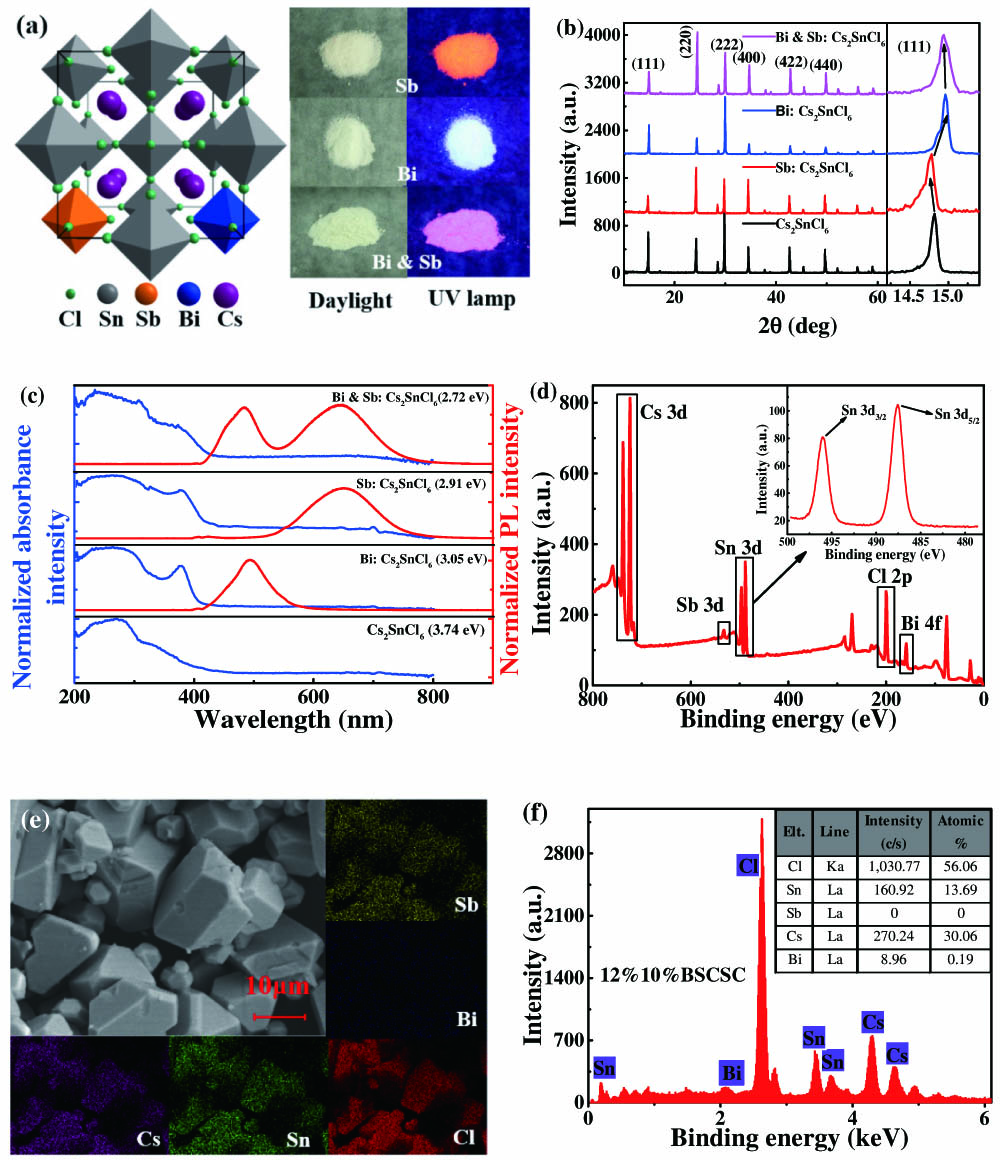
Figure 1.(a) Crystal structure of BSCSC MCs and the pictures of a series of sample under daylight and UV lamp. (b) XRD patterns of
![]()
Figure 2.PL spectra of BSCSC MCs with different (a) Bi and (b) Sb feeding contents. (c) PL spectra of 12%10%BSCSC MCs at 405 nm CW laser excitation under different pump fluences. (d) The linear fitting between PL intensity and pump fluence.
B. Steady-State PL Spectra at the Temperatures of 80–380 K
The optical properties of BSCSC MCs are characterized at room and low temperature. Figure 2(a) shows the steady-state PL spectra of 9% Bi and (, 30, and 40) Sb and 5.5%47% BSCSC under excitation wavelength of 360 nm. For a polarizable halide perovskite lattice structure, light-induced transient lattice deformation results in excitons being localized, which represents a type of bound state for efficient radiative recombination called STEs [12], Keeping Bi doping content unchanged, increasing the Sb doping content can get a gradual enhancement of orange PL emission. The enhancement in PL intensity may be attributed to the increase in Sb content leading to more STE production, which means more energy should belong to the [] transfer to STEs through intersystem crossing (ISC) [22]. There is no quenching phenomenon with high-concentration doping; it can be ruled out that the emission at 650 nm is attributed to ionoluminescence [23]. The broad spectra and the large Stokes shift of the peak position of 650 nm are attributed to STEs [24,25]. Figure 2(b) shows the PL spectra of (, 9, and 12) Bi and 10% Sb codoped MCs. There are fewer energy transfers to STEs with the increase of Bi feeding contents, and that makes the PL intensity of blue emission peak at 485 nm be gradually enhance. The blue emission is attributed to the [] defect complex at the luminescent centers, and almost no peak shift is consistent with previously reported [12]. PL spectra of 12%10%BSCSC MCs under different laser pump fluence are measured under the 405 nm CW laser at room temperature as shown in Fig. 2(c). The PL intensity increases gradually, and the FWHM has a slight increase with the pump laser fluence increasing from 35 to . With the material excited by laser for a long time, the surface temperature of the MCs is rising. The thermal effect has occurred, which causes a slight increase in the FWHM. The influence of pump fluence on PL intensity is shown in Fig. 2(d). The green and red solid lines are linear fitting curves with the spectrum integral intensity at the peak positions of 485 and 650 nm, the slopes of which are 0.80 and 0.75. The correlation coefficient () is 0.99, and the linear fitting curves reveal the existence of single-photon excitation.
The temperature-dependent PL spectra are efficient for studying the optical properties of materials, especially for understanding the luminous mechanism of substances [26]. As shown in Fig. 3, temperature-dependent PL measurements are performed for 12%10%BSCSC MCs within the temperature range of 80–380 K, which shows the same change as in the reported paper [27]. The small quantity of STEs is caused by weak electron–phonon interactions in a low-temperature environment, and the PL intensity is weakened. In the temperature range of 80–260 K, with the increase of temperature, the electron–phonon interactions are enhanced gradually, and more STEs are generated simultaneously [16]. In the range of 260–380 K, as the temperature continues to rise, the lattice vibration is enhanced. The lattice relaxation of the luminescent center increases, more phonons are coupled to excitons, and the nonradiative transition probability increases [25]. This leads to a reduction in luminous efficiency decrease, and the thermal quenching phenomenon begins to increase. The corresponding pseudocolor map is shown in Fig. 3(b), and it shows the PL intensity with the temperature rising, too. The temperature dependence of the integrated emission intensity can be described [28] as
![]()
Figure 3.(a) PL intensity of 12%10%BSCSC MCs at 80–380 K. (b) Pseudocolor map of PL intensity at 80–380 K. (c) The PL integral intensity of 12%10%BSCSC MCs at various temperatures. (d) The peak position with the change of temperature.
From 80 to 320 K, the photon energy or wavelength of the emission peak is almost a constant; this temperature-independent chromaticity makes them as a class of materials for potential application to cold-light LED.
C. TRPL Spectra at the Temperatures of 190–400 K
The TRPL of the two emission peaks needs to be measured. As shown in Fig. 4(a), the PL decay curve of 9%y%BSCSC (, 5, 10, and 20) MCs is measured at 485 nm excited by a 405 nm picosecond laser. Under the same synthesized condition that the content of Bi remains unchanged with the increase of Sb, the TRPL decay curve is fitted well by double exponential function Eq. (2):
![]()
Figure 4.(a) TRPL decay curves of 9%Bi
Figures 5(a) and 5(b) show the temperature-dependent TRPL decay curves at the wavelengths of 485 and 650 nm. More and more local electronic states promote the formation of STEs, which is caused by the fact that the substrate is 0D perovskite derivatives [37]. It shows the lifetime with the temperature rising in Fig. 5(c). Due to the weaker electron–phonon interaction at low-temperature conditions, the nonradiative recombination caused by free excitons is obvious in the temperature range from 80 to 260 K. With the increase of temperature, the electron–phonon interaction becomes stronger, and the PL decay is mainly dominated by STEs. When the temperature is higher than 300 K, thermal quenching makes the radiative recombination weaken and the nonradiative recombination strengthen, which results in the loss of lifetime. Figure 5(d) depicts a schematic energy diagram for BSCSC MCs. For undoped , the valence band maximum (VBM) is derived from Cl 3p states, while the conduction band minimum (CBM) consists of the antibonding states of Sn 5s and Cl 3p orbitals. When is codoped with Bi and Sb, it leads to the upward shift of VBM [12]. Furthermore, the lattice deformation makes the energy of the ground state rise, which increases the lattice deformation energy [38,39]. In the reported papers, there are a lot of ions with outermost electronic configuration acting as emission centers. Usually, there is a ground state with outer electrons . Triplet states (, 1, 2) and single state are formed by the splitting of the excited state. According to Hund’s rules, it can be arranged according to the excited state energy as . Due to electric and magnetic selection rules, the transitions of and are forbidden. The transitions of and are parity allowed due to spin-orbit coupling [24,40]. Due to the energy transition [22], part of energy belongs to [] transitions to STEs by ISC with the increase of Sb-doping content. In the process of energy transfer, part of the energy undergoes a radiative transition from to , exhibiting an emission at 485 nm. Due to ISC, part of the energy is transferred from to in a nonradiative way, and then it continues to be transferred to in the form of a radiative transition accompanied by a PL emission at 650 nm.
![]()
Figure 5.Temperature-dependent TRPL decay curves of 12%10%BSCSC MCs from 190 to 400 K at the wavelength of (a) 485 nm and (b) 650 nm. (c) PL lifetime with temperature increasing. (d) Schematic energy diagram for BSCSC MCs. (e) The lifetime of 485 nm emission under 290–390 K. (f)
In addition to the FIR, the PL decay lifetime with temperature dependence can also be used to apply in temperature measurement. To show the variation of the lifetime with temperature, the lifetime of 485 nm emission attributed to in the temperature range of 290–390 K is calculated as shown in Fig. 5(e). The relationship of lifetime and temperature can be fitted well by the Arrhenius equation [41]:
Figure 5(f) exhibits the change of and when the temperature rises. The maximum value of is determined to be at 345 K, which indicates higher sensitivity. The shows the same variation tendency, the maximum value of which is at 305 K. Table 1 summarizes some thermometric parameters about different sensing materials. Compared with and , Mn, the value of our sample based on the fluorescence lifetime technique is the highest, which means the sensitivity is pretty good. These parameters of high and show that this kind of material is suitable for noncontact temperature measurement. In short, these experiment results demonstrate that BSCSC MCs are promising for thermometry because of their outstanding sensitivity as well as excellent stability. Several Thermometric Materials and Their Relative SensitivityMaterials Probe Range Reference 120–570 2.08 [ 303–383 3.75 [ 298–373 0.9 [ 230–470 2.43 [ 290–390 3.82 This work
D. Optoelectronic Properties of WLEDs
Most WLED devices [44,45] are made by mixing perovskite powder with other commercial phosphors [30] in a proportion that contains rare-earth elements. The spectra of BSCSC MCs contain two emission peaks at 485 and 650 nm, of which the intensity can be controlled by different content, achieving the effect of controlling the color of light emission. The BSCSC MCs after grinding are mixed with a curable resin coat on a commercial UV-380 LED chip directly, and then the chip is dried at 50°C in a vacuum environment for 2 h to solidify the curable resin. Figure 6(a) shows the working WLED and the corresponding PL spectrum. Then the stability test of the WLED is carried out within 0–200 min. As shown in the inset of Fig. 6(a), it is concluded that the PL intensity can be maintained about at 68%. As seen in Fig. 6(b), the CIE coordinates of our WLED are located at (0.30, 0.37) with a color temperature of 6800 K after tuning the Bi and Sb feeding ratio (5.5%47%). The responding PL intensity increases with the increase of current, showing good stability. These properties make codoped Bi and Sb a promising candidate luminescent phosphor material.
![]()
Figure 6.(a) Electrically driven PL of white-emission LED based on Bi-and-Sb-codoped
4. CONCLUSIONS AND PERSPECTIVES
In summary, we successfully synthesized a series of BSCSC MCs with different Bi and Sb contents by using the solvothermal method. Compared with undoped MCs, dual broad emissions can be observed, of which emission peaks are located at 485 and 650 nm. Phonon–electron interaction and thermal quenching make the PL intensity exhibit the phenomenon of first strengthening and then weakening with the temperature rise. Temperature-dependent PL and TRPL reveal that 650 nm emission primarily originates from STEs due to the incorporation of Sb and the interconversion between radiative and nonradiative transition. The [] as the luminescent center is responsible for the 485 nm emission. The lifetime of this perovskite luminescence is used for noncontact temperature measurement for the first time. The maximum and values of and show better sensitivity than other materials, which indicates that there are application prospects in noncontact temperature measurement. By changing different feeding content of Bi and Sb to make phosphors and coating those on the 380 nm LED chip to make WLEDs, and adding no other commercial phosphors, this codoping provides a new idea for reducing costs in the future.
References
[1] C. Bi, Z. Yao, X. Sun, X. Wei, J. Wang, J. Tian. Perovskite quantum dots with ultralow trap density by acid etching-driven ligand exchange for high luminance and stable pure-blue light-emitting diodes. Adv. Mater., 33, 2006722(2021).
[2] T. Li, Q. Li, X. Tang, Z. Chen, Y. Li, H. Zhao, S. Wang, X. Ding, Y. Zhang, J. Yao. Environment-friendly antisolvent tert-amyl alcohol modified hybrid perovskite photodetector with high responsivity. Photon. Res., 9, 781-791(2021).
[3] M. Du, X. Zhu, L. Wang, H. Wang, J. Feng, X. Jiang, Y. Cao, Y. Sun, L. Duan, Y. Jiao, K. Wang, X. Ren, Z. Yan, S. Pang, S. Liu. High-pressure nitrogen-extraction and effective passivation to attain highest large-area perovskite solar module efficiency. Adv. Mater., 32, 2004979(2020).
[4] Y. Zhao, F. Ma, F. Gao, Z. Yin, X. Zhang, J. You. Research progress in large-area perovskite solar cells. Photon. Res., 8, A1-A15(2020).
[5] Z. Wu, J. Chen, Y. Mi, X. Sui, S. Zhang, W. Du, R. Wang, J. Shi, X. Wu, X. Qiu, Z. Qin, Q. Zhang, X. Liu. All-inorganic CsPbBr3 nanowire based plasmonic lasers. Adv. Opt. Mater., 6, 1800674(2018).
[6] S. Hussain, A. Raza, F. Saeed, A. Perveen, Y. Sikhai, N. Din, E. E. Elemike, Q. Huang, A. Subramanian, Q. Khan, W. Lei. Stable and high performance all-inorganic perovskite light-emitting diodes with anti-solvent treatment. Chin. Opt. Lett., 19, 030005(2021).
[7] Z. Chu, Q. Ye, Y. Zhao, F. Ma, Z. Yin, X. Zhang, J. You. Perovskite light-emitting diodes with external quantum efficiency exceeding 22% via small-molecule passivation. Adv. Mater., 33, 2007169(2021).
[8] T. C. Jellicoe, J. M. Richter, H. F. J. Glass, M. Tabachnyk, R. Brady, S. E. Dutton, A. Rao, R. H. Friend, D. Credgington, N. C. Greenham, M. L. Boehm. Synthesis and optical properties of lead-free cesium tin halide perovskite nanocrystals. J. Am. Chem. Soc., 138, 2941-2944(2016).
[9] P.-P. Sun, Q.-S. Li, L.-N. Yang, Z.-S. Li. Theoretical insights into a potential lead-free hybrid perovskite: substituting Pb2+ with Ge2+. Nanoscale, 8, 1503-1512(2016).
[10] L. Chu, W. Ahmad, W. Liu, J. Yang, R. Zhang, Y. Sun, J. Yang, X. A. Li. Lead-free halide double perovskite materials: a new superstar toward green and stable optoelectronic applications. Nano-Micro Lett., 11, 16-34(2019).
[11] M.-M. Yao, L. Wang, J.-S. Yao, K.-H. Wang, C. Chen, B.-S. Zhu, J.-N. Yang, J.-J. Wang, W.-P. Xu, Q. Zhang, H.-B. Yao. Improving lead-free double perovskite Cs2NaBiCl6 nanocrystal optical properties via ion doping. Adv. Opt. Mater., 8, 1901919(2020).
[12] Z. Tan, J. Li, C. Zhang, Z. Li, Q. Hu, Z. Xiao, T. Kamiya, H. Hosono, G. Niu, E. Lifshitz, Y. Cheng, J. Tang. Highly efficient blue-emitting bi-doped Cs2SnCl6 perovskite variant: photoluminescence induced by impurity doping. Adv. Funct. Mater., 28, 1801131(2018).
[13] J. Li, Z. Tan, M. Hu, C. Chen, J. Luo, S. Li, L. Gao, Z. Xiao, G. Niu, J. Tang. Antimony doped Cs2SnCl6 with bright and stable emission. Front. Optoelectron., 12, 352-364(2019).
[14] Y. Lin, L. Zhao, B. Jiang, J. Mao, F. Chi, P. Wang, C. Xie, X. Wei, Y. Chen, M. Yin. Temperature-dependent luminescence of BaLaMgNbO6: Mn4+, Dy3+ phosphor for dual-mode optical thermometry. Opt. Mater., 95, 109199(2019).
[15] M. D. Dramićanin, B. Milićević, V. Đorđević, Z. Ristić, J. Zhou, D. Milivojević, J. Papan, M. G. Brik, C. G. Ma, A. M. Srivastava, M. Wu. Li2TiO3:Mn4+ deep-red phosphor for the lifetime-based luminescence thermometry. ChemistrySelect, 4, 7067-7075(2019).
[16] S. Yang, S. Huang, Q. Wang, R. Wu, Q. Han, W. Wu. Temperature-dependent photoluminescence of Cs2Ag
[17] J. Luo, X. Wang, S. Li, J. Liu, Y. Guo, G. Niu, L. Yao, Y. Fu, L. Gao, Q. Dong, C. Zhao, M. Leng, F. Ma, W. Liang, L. Wang, S. Jin, J. Han, L. Zhang, J. Etheridge, J. Wang, Y. Yan, E. H. Sargent, J. Tang. Efficient and stable emission of warm-white light from lead-free halide double perovskites. Nature, 563, 541-545(2018).
[18] A. Yan, K. Li, Y. Zhou, Y. Ye, X. Zhao, C. Liu. Tuning the optical properties of Cs2SnCl6:Bi and Cs2SnCl6:Sb lead-free perovskites via post-annealing for white LEDs. J. Alloys Compd., 822, 153528(2020).
[19] R. Zeng, K. Bai, Q. Wei, T. Chang, J. Yan, B. Ke, J. Huang, L. Wang, W. Zhou, S. Cao, J. Zhao, B. Zou. Boosting triplet self-trapped exciton emission in Te(IV)-doped Cs2SnCl6 perovskite variants. Nano Res., 14, 1551-1558(2020).
[20] A. E. Maughan, A. M. Ganose, M. M. Bordelon, E. M. Miller, D. O. Scanlon, J. R. Neilson. Defect tolerance to intolerance in the vacancy-ordered double perovskite semiconductors Cs2SnI6 and Cs2TeI6. J. Am. Chem. Soc., 138, 8453-8464(2016).
[21] A. Kaltzoglou, M. Antoniadou, A. G. Kontos, C. C. Stoumpos, D. Perganti, E. Siranidi, V. Raptis, K. Trohidou, V. Psycharis, M. G. Kanatzidis, P. Falaras. Optical-vibrational properties of the Cs2SnX6 (X = Cl, Br, I) defect perovskites and hole-transport efficiency in dye-sensitized solar cells. J. Phys. Chem. C, 120, 11777-11785(2016).
[22] X. Liu, X. Xu, B. Li, L. Yang, Q. Li, H. Jiang, D. Xu. Tunable dual‐emission in monodispersed Sb3+/Mn2+ codoped Cs2NaInCl6 perovskite nanocrystals through an energy transfer process. Small, 16, 2002547(2020).
[23] B. Vargas, E. Coutiño-Gonzalez, O. Ovalle-Encinia, C. Sánchez-Aké, D. Solis-Ibarra. Efficient emission in halide layered double perovskites: the role of Sb3+ substitution in Cs4Cd1–
[24] V. Morad, Y. Shynkarenko, S. Yakunin, A. Brumberg, R. D. Schaller, M. V. Kovalenko. Disphenoidal zero-dimensional lead, tin, and germanium halides: highly emissive singlet and triplet self-trapped excitons and x-ray scintillation. J. Am. Chem. Soc., 141, 9764-9768(2019).
[25] Y. Jing, Y. Liu, M. Li, Z. Xia. Photoluminescence of singlet/triplet self-trapped excitons in Sb3+-based metal halides. Adv. Opt. Mater., 9, 2002213(2021).
[26] R. Wu, Q. Wang, S. Yang, L. Wu, S. Gong, Q. Han, W. Wu. Enhanced thermal stability of exciton recombination in CsPbI3 perovskite nanocrystals via zinc alloying. J. Alloys Compd., 857, 157574(2021).
[27] Y. Jing, Y. Liu, J. Zhao, Z. Xia. Sb3+ doping-induced triplet self-trapped excitons emission in lead-free Cs2SnCl6 nanocrystals. J. Phys. Chem. Lett., 10, 7439-7444(2019).
[28] W. Wu, W. Liu, Q. Wang, Q. Han, Q. Yang. Temperature-dependent photoluminescence of pure and Mn-doped CsPbCl3 nanocrystals. J. Alloys Compd., 787, 165-172(2019).
[29] Q. Wang, W. Wu. Temperature and excitation wavelength-dependent photoluminescence of CH3NH3PbBr3 crystal. Opt. Lett., 43, 4923-4926(2018).
[30] Q. Zhang, C. Diederichs, Q. Xiong. Golden hour for perovskite photonics. Photon. Res., 8, PP1-PP4(2020).
[31] X. Cheng, Z. Zang, K. Yuan, T. Wang, K. Watanabe, T. Taniguchi, L. Dai, Y. Ye. A hybrid structure light-emitting device based on a CsPbBr3 nanoplate and two-dimensional materials. Appl. Phys. Lett., 116, 263103(2020).
[32] Q. Wang, W. Wu, R. Wu, S. Yang, Y. Wang, J. Wang, Z. Chai, Q. Han. Improved thermal stability of photoluminescence in Cs4PbBr6 microcrystals/CsPbBr3 nanocrystals. J. Colloid Interface Sci., 554, 133-141(2019).
[33] M. Baranowski, P. Plochocka, R. Su, L. Legrand, T. Barisien, F. Bernardot, Q. Xiong, C. Testelin, M. Chamarro. Exciton binding energy and effective mass of CsPbCl3: a magneto-optical study. Photon. Res., 8, A50-A55(2020).
[34] X. K. Gong, X. S. Zhang, X. Liu, R. K. Ding, J. J. Zhang, H. Yin, Z. W. Zhang, L. Li, J. P. Xu. Novel cryogenic dual-emission mechanism of lead-free double perovskite Cs2AgInCl6 and using SiO2 to enhance their photoluminescence and photostability. J. Hazard. Mater., 403, 123821(2021).
[35] B. Ke, R. Zeng, Z. Zhao, Q. Wei, X. Xue, K. Bai, C. Cai, W. Zhou, Z. Xia, B. Zou. Homo- and heterovalent doping-mediated self-trapped exciton emission and energy transfer in Mn-doped Cs2Na1-
[36] G. Xiong, L. Yuan, Y. Jin, H. Wu, Z. Li, B. Qu, G. Ju, L. Chen, S. Yang, Y. Hu. Aliovalent doping and surface grafting enable efficient and stable lead-free blue-emitting perovskite derivative. Adv. Opt. Mater., 8, 2000779(2020).
[37] S. Li, J. Luo, J. Liu, J. Tang. Self-trapped excitons in all-inorganic halide perovskites: fundamentals, status, and potential applications. J. Phys. Chem. Lett., 10, 1999-2007(2019).
[38] B. Yang, X. Mao, F. Hong, W. Meng, Y. Tang, X. Xia, S. Yang, W. Deng, K. Han. Lead-free direct band gap double-perovskite nanocrystals with bright dual-color emission. J. Am. Chem. Soc., 140, 17001-17006(2018).
[39] X. Wang, W. Meng, W. Liao, J. Wang, R. G. Xiong, Y. Yan. Atomistic mechanism of broadband emission in metal halide perovskites. J. Phys. Chem. Lett., 10, 501-506(2019).
[40] H. Arfin, A. S. Kshirsagar, J. Kaur, B. Mondal, Z. Xia, S. Chakraborty, A. Nag. ns2 electron (Bi3+ and Sb3+) doping in lead-free metal halide perovskite derivatives. Chem. Mater., 32, 10255-10267(2020).
[41] F. Li, J. Cai, F. Chi, Y. Chen, C. Duan, M. Yin. Investigation of luminescence from LuAG: Mn4+ for physiological temperature sensing. Opt. Mater., 66, 447-452(2017).
[42] L. Marciniak, K. Trejgis. Luminescence lifetime thermometry with Mn3+-Mn4+ co-doped nanocrystals. J. Mater. Chem. C, 6, 7092-7100(2018).
[43] M. Sekulić, V. Đorđević, Z. Ristić, M. Medić, M. D. Dramićanin. Highly sensitive dual self-referencing temperature readout from the Mn4+/Ho3+ binary luminescence thermometry probe. Adv. Opt. Mater., 6, 1800552(2018).
[44] S. Huang, S. Yang, Q. Wang, R. Wu, Q. Han, W. Wu. Cs4PbBr6/CsPbBr3 perovskite composites for WLEDs: pure white, high luminous efficiency and tunable color temperature. RSC Adv., 9, 42430-42437(2019).
[45] W. Wang, D. Wang, F. Fang, S. Wang, G. Xu, T. Zhang. CsPbBr3/Cs4PbBr6 Nanocomposites: formation mechanism, large-scale and green synthesis, and application in white light-emitting diodes. Crystal Growth Des., 18, 6133-6141(2018).

Set citation alerts for the article
Please enter your email address
© Copyright 2018-2021 | Chinese Laser Press. All Rights Reserved 沪ICP备15018463号-20