
Lemeng Leng, Zhaobang Zeng, Guihan Wu, Zhongzhi Lin, Xiang Ji, Zhiyuan Shi, Wei Jiang. Phase calibration for integrated optical phased arrays using artificial neural network with resolved phase ambiguity[J]. Photonics Research, 2022, 10(2): 347
- Photonics Research
- Vol. 10, Issue 2, 347 (2022)
Abstract
1. INTRODUCTION
Integrated optical phased arrays (OPAs) can control the propagating behavior of light in free space without bulky mechanical components, showing great potential in applications such as light detection and ranging (lidar), wireless optical communication, and image projection [1–24]. Owing to the complementary metal oxide semiconductor-compatible (CMOS) processes, a large number of components can be readily integrated on-chip, forming a compact phased array system. The optical paths of the elements of an integrated OPA are generally designed with fan-in waveguides to form an aligned wavefront as an initial state [1–3]. However, the high index contrast of silicon waveguides always results in substantial random phase errors in the paths of the waveguides due to fabrication variation, which generates a distorted far-field pattern different from the ideal initial state. These fabrication-induced phase errors are generally compensated for by adding an extra phase shift determined from optimal searching methods such as the particle swarm optimization (PSO) algorithm, gradient descent algorithm, and genetic algorithm [12–23]. Such an iterative, optimization-based calibration process is able to align the wavefront and to achieve reasonably good results in practice. However, the phase calibration process is always time-consuming. Recently, encouraging improvements of the calibration accuracy and efficiency have been demonstrated by modifying the algorithm, using an on-chip monitor or interference-assisted setup [24–27], although the core algorithms remain based on an iterative search of the optimum in a high-dimensional space. For a large number of OPA device samples that are needed in real applications, the lengthy iteration process needs to be repeated for each sample, which can result in prohibitive time and cost for calibration [for an illustrative example, see Appendix D, Fig. 10(c)].
For an OPA, it would be desirable to identify the phase error distribution among the OPA elements from the irregular far-field pattern instantly and calibrate the device to an ideal initial state without prolonged iterative processes. However, it is difficult to inversely solve the complex nonlinear relationship between the far-field pattern and near-field phase distribution to find the phase errors in such a photonic system. Recently, the artificial neural network (ANN) has provided new solutions for many subjects such as nanophotonic designs [28], identifying the different phases of matter [29], and solving ellipsometric problems [30]. Its ability to deal with complex nonlinear mapping makes it an ideal building block of a framework to solve the inverse problem for OPA calibration. In this work, we demonstrate an ANN-assisted method to identify the phase error distribution among OPA elements and calibrate an OPA. As we shall see, phase ambiguity is a pivotal problem in the OPA system that may prevent the efficacy of the ANN. Device-physics analysis of the OPA can offer insight to overcome ambiguity-induced problems. Combining the ANN and OPA device-physics analysis, we experimentally demonstrate a rapid, iteration-free calibration approach.
2. ANN FOR OPA CALIBRATION
The devices we propose to calibrate are designed and fabricated on a silicon-on-insulator (SOI) wafer. Figure 1(a) schematically shows the OPA consisting of a grating coupler for input coupling, multimode interferences (MMIs) tree for power splitting, thermo-optic phase shifters, and a dense output waveguide array (see details in Appendix A). The operation wavelength is set to be . There are phase shifters in this device to control the relative phase of elements . The first element is considered as a reference channel, to exploit the freedom of setting a reference phase. Hence, the output phase error distribution of elements is
Sign up for Photonics Research TOC. Get the latest issue of Photonics Research delivered right to you!Sign up now
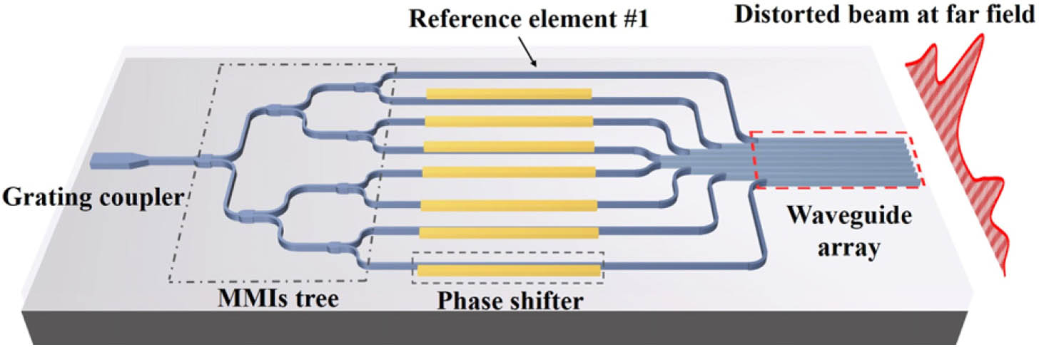
Figure 1.Schematic view of an integrated OPA, along with the far-field pattern.
The relative phase error distributions are ubiquitous and unpredictable on different devices fabricated in a batch. For the integrated waveguides, fabrication-induced phase errors (e.g., due to random fluctuations of the waveguide widths and hence propagation constants) accumulate along the propagation lengths of waveguides, which is unavoidable. Other possible contributions to phase errors are discussed in Appendix A. The total phase errors need to be treated. Note that the far-field beam profile remains unchanged for any phase to change by a multiple of . Hence, we only need to consider the phase error of each element in the range of [0, ). To align the wavefront for all elements, we first build an ANN model to identify the phase errors from the unordered far-field patterns directly. We generate the data set according to the phased array theory [31]. The normalized far-field intensity pattern of the -element phased array can be calculated using the following equations:
![]()
Figure 2.Example of the far-field patterns for feeding the neural network,
Then we build the Net 1, as shown in Fig. 2(c). The sizes of the input and output layers are and , respectively, corresponding to the number of points in the far-field patterns and the relative phase errors of elements , as shown in Fig. 2(a). The input layer with neurons and hidden layers, each with neurons, are connected with a sigmoid activation function to build a forward-propagated neural network. Here represents the total number of the hidden layers. We also use a sigmoid function to normalize the output in range of [0, 1]. The predicted phase errors can be recovered by multiplying the output by . A loss function of mean square error (MSE) between the predicted phase errors and the real phase errors is selected to train the model, which is defined as
3. RESOLVE AMBIGUITY IN THE ANN MODEL OF AN OPA
Training loss and validation loss of the Net 1 cannot achieve convergence to a small value after 2500 epochs, as shown in Fig. 3(a). OPA-oriented device-physics analysis shows that this is caused by the phase ambiguity in the OPA cast into the ANN model. The ANN model is trained to build a functional relationship between the input and output layers, which in principle requires a one-to-one mapping. As presented by Eqs. (1)–(4), the far-field pattern of the OPA mainly depends on the phase error distribution of . However, considering another conjugate phase error distribution of , the corresponding is given by
![]()
Figure 3.Loss of (a) Net 1, (b) Net 2, (c) Net 3, and (d) Net 4 with the architecture in Figs.
Due to the symmetric position of the waveguide-based emitters (), equals , based on Eq. (3). Hence can be written as
Comparing Eqs. (2) and (6), magnitudes of and are totally identical at the far field, since . Consequently, the Net 1 cannot find the right direction between two conjugate cases to minimize the loss, and then build an inaccurate mapping from far-field patterns to the phase labels in the data set during training. In this case, the ANN output phase error distribution will be some sort of “intermediate state” between two conjugate distributions. As these two conjugate cases ( and ) reverse their spatial orders of error sequence and change the signs, their distance in the -dimensional phase error distribution space is usually fairly large. Thus, the “intermediate state” given by the ANN output (the “interpretation” of “intermediate” is network-dependent) is likely far from either or . One can readily see from Eqs. (1)–(3) that the OPA beam profiles calibrated by , , or their intermediate state will generally differ drastically also.
In order to resolve ambiguity caused by the conjugate phase distribution, we introduce an additive pattern 2, , by tuning the phase shifters of element with a virtual phase mask of on top of the intrinsic relative random phase error distribution, as shown in Fig. 2(b). The additive pattern, , can be calculated by
For the conjugate phase error distribution, in Eq. (8) is given by
Comparing Eqs. (8) and (9), and are evidently different. Based on the analysis above, the combined far-field intensity patterns in a conjugate pair, , provide more features for the ANN to resolve the corresponding phase label, , from the ambiguous label . Note that there is no phase shifter in element #1 for which we use an equivalent phase mask as to achieve the same effect. Figure 2(b) shows a sample of input data generated by using the phase mask with data points.
Meanwhile, the output for such an optical system is a periodic function of phase, which is intractable for a standard neural network with a fixed output range, e.g., [0, ). For instance, consider whether one of the actual phase errors is . Within the computing/training accuracy, the network may find both and correspond to roughly the same beam pattern according to Eqs. (1)–(3). However, and are very far on the axis, and the network believes that they must belong to two different states, which results in confusion. Fundamentally, the intrinsic continuity of the mapping function at the two ends of this interval [0, ) is lost, which can baffle the otherwise obvious convergence. To resolve such periodic ambiguity while retaining the intrinsic continuity, we transform the real phase errors, , and the predicted errors, , into the complex domain by defining
Then the continuity-preserving loss function (via a certain form of complex mean square error, or CMSE) is written as
Then, we construct the Net 2, Net 3, and Net 4 in Figs. 2(d)–2(f) with different network architectures or loss functions to tackle the ambiguities. The architectures of Net 2 and Net 1 are identical, but we introduce the CMSE loss function for Net 2 to solve the periodic ambiguity only, as indicated by the purple arrow in Fig. 2(e). The sizes of the hidden layers and output layers of Net 3 and Net 4 are identical with Net 1 and Net 2, respectively. The difference is that Net 3 and Net 4 use the combination of pattern1 and pattern 2 in Figs. 2(a) and 2(b) in conjugate pair to solve the conjugate ambiguity. The sizes of the input layers for these two nets increase to , as illustrated with different colors in Figs. 2(d) and 2(f). Hence, Net 4 using CMSE can solve both conjugate ambiguity and periodic ambiguity. It should be noted that the data set for ANN using the loss function, CMSE, is totally compatible with the one for ANN using a loss function of MSE. So, we train the Net 2 with the single-pattern data set the same as Net 1 (input dimension: ). Net 3 and Net 4 are trained using same data set with an input dimension of and output dimension of .
After training, the validation loss of Net 1 and Net 2 (single beam profile input) cannot achieve convergence. Meanwhile, when comparing the red curves in Figs. 3(a) and 3(c), MSE loss of Net 3 finally converges to a lower level () than that of Net 1 using the loss function of MSE, indicating that the negative effect of the conjugate ambiguity during the training process has been eliminated. From Figs. 3(c) and 3(d), the periodic ambiguity is further removed. As shown in Fig. 3(d), the validation loss of Net 4 decreases to 0.04 (from in Net 1), which indicates the high efficacy enabled by removing the conjugate ambiguity and periodic ambiguity. Here, the time for generating the two data sets (single-pattern and dual-pattern) is all below . Additionally, due to the different complexity of the input layer, it takes about 2.5 h for Net 1 and Net 2 and about 3 h for Net 3 and Net 4 to complete the training process over 2500 epochs.
To further demonstrate the performance of the ANN models, we simulate far-field patterns before and after calibration according to the phase error distributions predicted by Net 1 to Net 4, using four arbitrary samples in the testing data set. Figures 4(a1)–4(a4) show the far-field patterns calculated by the phase error data in the four samples. The irregular far-field profiles in Figs. 4(b1)–4(b4) and 4(c1)–4(c4) illustrate that Net 1 and Net 2 cannot output valid phase distributions, due to the conjugate ambiguity. Meanwhile, the performance of Net 3 is better than we have expected, even if the validation loss after training is only around 0.9. It can still align the wavefront for the testing samples of ii) and iii) and form perfect beams pointed to 0° with side lobe suppression ratio (SLSR) of 12.29 dB and 12.75 dB, as shown in Figs. 4(d2) and 4(d3). However, the poor SLSRs in Figs. 4(d1) and 4(d4), caused by several incorrect elements, indicate the limited capability of MSE-based ANN. By analyzing the residual phase error data in the samples ii) and iii), Net 3 cannot accurately predict the phase of the elements which is close to 0 or , which is consistent with our previous analysis on the periodic ambiguity. Finally, Figs. 4(e1)–(e4) present the beams calibrated by Net 4 with average SLSR of about 12.7 dB, showing the high accuracy of Net 4 (see more detail in Fig. 8 in Appendix C), with both conjugate and periodic ambiguities resolved.
![]()
Figure 4.Simulated performance of the ANNs using four randomly selected samples i) to iv) in testing set. Each sample is signified with a different color. (a1)–(a4) Far-field profiles before calibration. Beam profiles after calibration from the output of (b1)–(b4) Net 1; (c1)–(c4) Net 2; (d1)–(d4) Net 3; and (e1)–(e4) Net 4. The sidelobe levels of the formed beams are noted in (d1)–(d4) and (e1)–(e4). All figures share the same axis.
Hence, as we analyzed above, the enhanced training data set using far-field patterns in a conjugate pair and continuity-preserving loss function are indispensable elements for building such an ANN for phase calibration. It is important to point out that the elimination of symmetrical-array-induced conjugate ambiguity is a crucial factor to construct the unique mapping between the input layer and output layer. And the loss function CMSE introduced here to deal with periodic ambiguity can significantly improve the network performance as a supplemental approach.
4. EXPERIMENT
Figure 5 shows the experimental setup for automatic phase calibration based on the well-trained ANN. The optical signal output from a 1550-nm laser is coupled to the grating coupler in the device by a single-mode fiber via a polarization controller. The far-field patterns are measured using a mechanically rotated detector, 10 cm away from the end face of the chip. During motion, the detector continuously samples the light intensity from to , and a far-field pattern is obtained and then transferred to the computer. A multichannel current source controlled by the computer provides driving power for the electrodes on the chip via 16 channel probes.
![]()
Figure 5.Schematic of the experimental setup for automatic calibration via Net 4 (FPC, fiber polarization controller; SMF, single-mode fiber).
To verify the effectiveness of our approach, we arbitrarily chose two OPA devices fabricated on the same wafer to calibrate the mismatched wavefront. First, we measure the far-field pattern without applying electric power to the phase shifters. Then we control the current source to uniformly apply a driving power of to the phase shifters for the elements #2–#16 and obtain the far-field pattern . Figure 7(b) in Appendix A shows the typical power-phase characteristic of the phase shifter as we vary the heating power. Once the far-field patterns in a conjugate pair are fed to the trained ANN model, it will predict the phase errors for each element. Then the computer automatically calculates the complementary heating power for calibrating the devices and then controls the electric source output driving current for each phase shifter to automatically align the wavefront.
The normalized far-field patterns in blue lines with multiple sidelobes in Figs. 6(a) and 6(d) are measured before calibration for the two devices, reflecting significant wavefront mismatch and variability in different dies. The red curves in Figs. 6(a) and 6(d) indicate the calculated beam profiles according to the phase error output from the ANN model. For device i), profiles of the highest and second-highest lobes in the measured far-field pattern at 0° and 49° are showing excellent agreement with the calculated pattern. Similar excellent agreement of the lobes at , 16°, and 39° can also be observed from far-field patterns in device ii). In addition, positions of the measured lobes of lower levels are also in good agreement with the calculated patterns. Generally, this method ensures that the highest lobes agree well; the fairly small deviations in the lower lobes are due to potential small nonuniformities/noise (see discussion in Appendix C). Figures 6(b) and 6(e) show the measured beams of the two devices after calibration according to the phase error output from the ANN model, along with 12.67 and 12.29 dB SLSR in the entire field of view (180°). Figures 6(c) and 6(f) present the beams of the two devices using the PSO algorithm with 12.46 and 11.73 dB SLSR, which are in reasonable agreement with the ANN results.
![]()
Figure 6.Calibration for two arbitrarily selected devices i) and ii); experimentally measured far-field pattern before calibration (blue line) and calculated far-field pattern (red line) using the ANN-predicted phase error for (a) device i) and (d) device ii); measured beam profile after calibration using ANN for (b) device i) and (e) device ii); condensed beam profile after calibration using PSO for (c) device i) and (f) device ii).
5. DISCUSSION AND CONCLUSION
In terms of the calibration results, the beam profiles after calibration by PSO and ANN-assisted methods both show reasonable agreement with the simulation. But the ANN model is significantly more efficient in time than an iterative optimization approach such as the PSO. In this case, the PSO-based calibration roughly needs iterations in experiment to achieve convergence with 200 far-field measurements per iteration (for 200 swarm elements), which is measurements in total for one OPA device. Simulated statistics over 500 OPA devices show that the PSO approach can achieve a moderate root-mean-square phase error (RMSE) with far-field measurements (see more detail in Appendix D). By comparison, this ANN-assisted method can instantly recognize the phase error distributions and calibrate the devices to achieve a relatively smaller phase error, (see Fig. 8 in Appendix C) in merely two far-field measurements per device, which is several orders of magnitude more efficient. Note that it is possible to reduce the number of iterations for the iterative optimal search approaches at the cost of calibration accuracy (or using nonevolutionary iterative search approaches at the cost of likelihood of approaching the global optimum). However, for the comparable calibration accuracy, this ANN-assisted approach is generally significantly more efficient. For a proof-of-principle demonstration, we use a 16-element 1D OPA here due to fabrication and test-equipment cost concerns. The principle demonstrated here can be readily applied to an OPA of any size, including 2D cases (OPAs of 1D or 2D share the same working principle). For a 2D OPA, one readily sees that both the conjugate ambiguity and periodic ambiguity occur similarly and can be treated similarly using the approaches shown here. For different OPA structures (or with a different number of elements), the ANN should be trained again with regenerated data sets. Note that while it takes some time to train the ANN, the calibration time per device is extremely short after training, and postcalibration performance variation is very small [see Fig. 10(b) in Appendix D]. Hence the ANN-based calibration is preferred in real-world applications where a large batch of OPA devices with the same design can be calibrated almost in real time with only one-time training of the ANN. For a proof-of-principle demonstration, we only use a sigmoid function, which performs well with the current ANN. If other network architectures (or different network depths) are used, other activation functions such as the rectified linear unit (ReLU) might be preferred [32]. As our ANN-assisted noniterative approach works for the full phase error range (), it may also be potentially useful in solving similar problems in related topics (e.g., Ref. [33]).
Note that many phase-retrieval techniques [34–36] have been developed with great success by considering the relation between the diffraction plane and image plane with spatial resolution of phase variation usually much larger than the wavelength. For the half-wavelength pitch OPA studied here, the spatial resolution of phase variation is a half-wavelength, and the corresponding radiation angles are far off the optical axis (up to 90°), which represents a regime seldom studied before in phase retrieval. Furthermore, OPA applications require a phase calibration metric of SLSR over the full field of 180°, which is seldom considered in phase retrieval. Also, in Eqs. (1)–(3), we have used a formalism not based on Fourier transform to deal with the special needs (far off-axis radiation) in our OPA calibration, whereas conventional phase retrieval usually uses Fourier transform. The phase diversity technique in phase retrieval uses a phase distortion to generate a second image for use together with the original image, for purposes such as combating image blurring [37,38]. Our approach to resolving the conjugate ambiguity appears similar to that technique in the aspect of taking more than one “imaging” measurement (note: an “imaging” measurement is just a far-field measurement here). However, we theoretically reveal the exact need of one extra measurement for a different application—OPAs. For an OPA with radiation angles up to 90° (a regime seldom studied in phase retrieval), we have presented conjugate ambiguity analysis: proving the conjugate ambiguity resolution in OPAs needs exactly two imaging measurements. In contrast, three or more imaging measurements [38] may be needed in conventional phase retrieval for different reasons.
Deep learning (or neural networks) has also been introduced into phase retrieval and has shown great promise [39–41]. However, it has not altered the aspects of low spatial resolution of phase variation and small off-axis angles of conventional methods. Note that many common assumptions for routine phase retrieval need to be revised for subwavelength spatial resolution (or high spatial frequency, or far off-axis cases). Considering the nonlinearity in the problem, nontrivial efforts are needed to adapt conventional phase-retrieval methods to achieve the same efficiency and accuracy (judged by the SLSR metric for OPAs) in the regime of subwavelength spatial resolution. Note that many things that can be easily done at large scales can be extremely difficult at subwavelength scales.
In summary, we have demonstrated a noniterative phase calibration approach based on machine-learning technology for integrated OPAs. Thanks to device-physics-based analysis that helps resolve conjugate ambiguity and periodic ambiguity in phase, the well-trained ANN model is able to identify the phase error distributions and retrieve initial working state for the OPAs from merely two measurements of the far-field patterns. Compared with the iterative calibration methods, our neural-network-assisted approach is highly efficient, noniterative, and suitable for calibration of a massive set of device samples. As myriads of lidars are envisioned to be needed in future widespread deployment of self-driving cars, this work may potentially provide a key foundation for rapid, massive calibration of OPA devices with high-quality beam characteristics for widespread use of lidars.
APPENDIX A: DEVICE STRUCTURE, FABRICATION, AND TESTING
The OPA is fabricated on SOI wafers with 2 μm buried oxide and a 220 nm top silicon layer. Three steps of etching are utilized to fabricate the grating coupler, MMIs, and waveguides. The etched structure is then covered by a 3-μm-thick layer for surface protection and for isolating the optical waveguide from metal layers. A waveguide superlattice with an interwaveguide pitch of 0.8 μm is arranged periodically to form the emitters at the end face of the chip with cross talk below [
Note that OPAs with an emitter pitch larger than a half-wavelength (e.g., some OPAs with grating emitters) will generate strong grating lobes at the far field. In practice, such OPAs generally work only in the range of and , where the strong grating lobes are absent. As the input angular pattern to the ANN is limited to this range with no strong grating lobes, our approach can be readily adapted to such OPAs in practice. It is well known the far-field pattern outside this range can be deterministically related to the pattern in this range; hence, the pattern in this range should contain sufficient information to solve for the phase deviation.
APPENDIX B: SUPPORTING EXPERIMENTAL DATA FOR SINGLE-CHANNEL PHASE CHARACTERISTICS
Before calibration, we first measure resistance of the elements #2–#16 through multipin probes for the tested device #1, shown in Fig.
![]()
Figure 7.(a) Measured resistances of the phase shifters in our 16-channel OPA; (b) measured (scatter) and fitted (line) heating power versus output intensity for the phase shifter embedded in an interferometer.
Then, phase versus heating power relationship for the thermo-optic phase shifter of the OPA is obtained by embedding an identical phase shifter in one arm of an integrated Mach–Zehnder interferometer (as in a thermo-optic switch) fabricated together with the OPA. The output intensity versus heating power relation of the switch, along with the fitted sinusoidal curve, as shown in Fig.
APPENDIX C: ACCURACY AND ROBUSTNESS OF THE NETWORK
For the ANN we present in Fig.
![]()
Figure 8.Distribution of calculated
![]()
Figure 9.Accuracy of the ANN versus
APPENDIX D: Calibration Efficiency of the PSO and ANN
In order to illustrate the time efficiency of our noniterative method, we simulate the calibration process using PSO with 500 OPA devices in the test data set. Actually, the performance of the PSO algorithm is mostly dependent on the swarm size (number of elements in the swarm). Figure
![]()
Figure 10.Simulated PSO-based calibration statistics for 500 OPA devices, compared with ANN-model test results. (a) Simulated accuracy of the test set using PSO algorithms with different swarm sizes (the accuracy of ANN is marked for comparison); (b) simulated sidelobe suppression ratio statistics (the average and very small standard deviation of ANN are marked by a red line and a narrow shaded stripe, respectively); (c) total number of experimental evaluations (equivalent to the number of far-field measurements) required for this iterative method for 500 OPA devices. Note that the
For comparison, for our ANN-assisted calibration method, the calibration accuracy () in Fig.
APPENDIX E: BEAM CHARACTERISTIC OF THE END-FIRE OPA
Note that the current OPA in an end-fire configuration forms line-like beams extending vertically at the far field. Figure
![]()
Figure 11.Measured 2D beam profiles (a) before calibration, (b) after calibration using ANN, and (c) after calibration using PSO for device i) in Fig.
References
[1] K. Van Acoleyen, W. Bogaerts, J. Jágerská, N. Le Thomas, R. Houdré, R. Baets. Off-chip beam steering with a one-dimensional optical phased array on silicon-on-insulator. Opt. Lett., 34, 1477-1479(2009).
[2] D. Kwong, A. Hosseini, Y. Zhang, R. T. Chen. 1 × 12 unequally spaced waveguide array for actively tuned optical phased array on a silicon nanomembrane. Appl. Phys. Lett., 99, 051104(2011).
[3] D. Kwong, A. Hosseini, J. Covey, Y. Zhang, X. Xu, H. Subbaraman, R. T. Chen. On-chip silicon optical phased array for two-dimensional beam steering. Opt. Lett., 39, 941-944(2014).
[4] C. T. DeRose, R. D. Kekatpure, D. C. Trotter, A. Starbuck, J. R. Wendt, A. Yaacobi, M. R. Watts, U. Chettiar, N. Engheta, P. S. Davids. Electronically controlled optical beam-steering by an active phased array of metallic nanoantennas. Opt. Express, 21, 5198-5208(2013).
[5] J. Sun, E. Timurdogan, A. Yaacobi, E. S. Hosseini, M. R. Watts. Large-scale nanophotonic phased array. Nature, 493, 195-199(2013).
[6] W. Ke, N. Ampalavanapillai, L. Christina, W. Elaine, A. Kamal, L. Hongtao, S. Efstratios. High-speed indoor optical wireless communication system employing a silicon integrated photonic circuit. Opt. Lett., 43, 1323-1326(2018).
[7] J. Midkiff, K. M. Yoo, J.-D. Shin, H. Dalir, M. Teimourpour, R. T. Chen. Optical phased array beam steering in the mid-infrared on an InP-based platform. Optica, 7, 1544-1547(2020).
[8] P. Wang, A. Kazemian, X. Zeng, Y. Zhuang, Y. Yi. Optimization of aperiodic 3D optical phased arrays based on multilayer Si3N4/SiO2 platforms. Appl. Opt., 60, 484-491(2021).
[9] H. Ito, Y. Kusunoki, J. Maeda, D. Akiyama, N. Kodama, H. Abe, R. Tetsuya, T. Baba. Wide beam steering by slow-light waveguide gratings and a prism lens. Optica, 7, 47-52(2020).
[10] N. Dostart, B. Zhang, A. Khilo, M. Brand, K. A. Qubaisi, D. Onural, D. Feldkhun, K. H. Wagner, M. A. Popovi. Serpentine optical phased arrays for scalable integrated photonic LIDAR beam steering. Optica, 7, 726-733(2020).
[11] W. Song, R. Gatdula, S. Abbaslou, M. Lu, A. Stein, Y. C. Lai, J. Provine, R. F. W. Pease, D. N. Christodoulides, W. Jiang. High-density waveguide superlattices with low crosstalk. Nat. Commun., 6, 7027(2015).
[12] J. C. Hulme, J. K. Doylend, M. J. R. Heck, J. D. Peters, M. L. Davenport, J. T. Bovington, L. A. Coldren, J. E. Bowers. Fully integrated hybrid silicon two dimensional beam scanner. Opt. Express, 23, 5861-5874(2015).
[13] C. V. Poulton, M. J. Byrd, P. Russo, E. Timurdogan, M. Khandaker, D. Vermeulen, M. R. Watts. Long-range LiDAR and free-space data communication with high-performance optical phased arrays. IEEE J. Sel. Top. Quantum Electron., 25, 7700108(2019).
[14] F. Aflatouni, B. Abiri, A. Rekhi, A. Hajimiri. Nanophotonic projection system. Opt. Express, 23, 21012-21022(2015).
[15] C. T. Phare, M. Shin, S. A. Miller, B. Stern, M. Lipson. Silicon optical phased array with high-efficiency beam formation over 180 degree field of view(2018).
[16] J. K. Doylend, M. J. R. Heck, J. T. Bovington, J. D. Peters, L. A. Coldren, J. E. Bowers. Two-dimensional free-space beam steering with an optical phased array on silicon-on-insulator. Opt. Express, 19, 21595-21604(2011).
[17] Y. Zhang, Y.-C. Ling, K. Zhang, C. Gentry, D. Sadighi, G. Whaley, J. Colosimo, P. Suni, S. J. Ben Yoo. Sub-wavelength-pitch silicon-photonic optical phased array for large field-of-regard coherent optical beam steering. Opt. Express, 27, 1929-1940(2019).
[18] S. A. Miller, Y.-C. Chang, C. T. Phare, M. C. Shin, M. Zadka, S. P. Roberts, B. Stern, X. Ji, A. Mohanty, O. A. Jimenez Gordillo, U. D. Dave, M. Lipson. Large-scale optical phased array using a low-power multi-pass silicon photonic platform. Optica, 7, 3-6(2020).
[19] W. Xu, L. Zhou, L. Lu, J. Chen. Aliasing-free optical phased array beam-steering with a plateau envelope. Opt. Express, 27, 3354-3368(2019).
[20] S.-H. Kim, J.-B. You, Y.-G. Ha, G. Kang, D.-S. Lee, H. Yoon, D.-E. Yoo, D.-W. Lee, K. Yu, C.-H. Youn, H.-H. Park. Thermo-optic control of the longitudinal radiation angle in a silicon-based optical phased array. Opt. Lett., 44, 411-414(2019).
[21] P. Wang, G. Luo, Y. Xu, Y. Li, Y. Su, J. Ma, R. Wang, Z. Yang, X. Zhou, Y. Zhang, J. Pan. Design and fabrication of a SiN-Si dual-layer optical phased array chip. Photon. Res., 8, 912-919(2020).
[22] D. N. Hutchison, J. Sun, J. K. Doylend, R. Kumar, J. Heck, W. Kim, C. T. Phare, A. Feshali, H. Rong. High-resolution aliasing-free optical beam steering. Optica, 3, 887-890(2016).
[23] L.-M. Leng, Y. Shao, P.-Y. Zhao, G.-F. Tao, S.-N. Zhu, W. Jiang. Waveguide superlattice-based optical phased array. Phys. Rev. Appl., 15, 014019(2021).
[24] S. Chung, M. Nakai, S. Idres, Y. Ni, H. Hashemi. 19.1 optical phased-array FMCW LiDAR with on-chip calibration. IEEE International Solid-State Circuits Conference (ISSCC), 286-288(2021).
[25] T. Komljenovic, P. Pintus. On-chip calibration and control of optical phased arrays. Opt. Express, 26, 3199-3210(2018).
[26] J. Shim, J.-B. You, H.-W. Rhee, H. Yoon, S.-H. Kim, K. Yu, H.-H. Park. On-chip monitoring of far-field patterns using a planar diffractor in a silicon-based optical phased array. Opt. Lett., 45, 6058-6061(2020).
[27] H. Zhang, Z. Zhang, C. Peng, W. Hu. Phase calibration of on-chip optical phased arrays via interference technique. IEEE Photon. J., 12, 6600210(2020).
[28] J. Peurifoy, Y. Shen, L. Jing, Y. Yang, F. Cano-Renteria, B. G. DeLacy, J. D. Joannopoulos, M. Tegmark, M. Soljačić. Nanophotonic particle simulation and inverse design using artificial neural networks. Sci. Adv., 4, eaar4206(2018).
[29] J. Carrasquilla, R. G. Melko. Machine learning phases of matter. Nat. Phys., 13, 431-434(2017).
[30] J. Liu, D. Zhang, D. Yu, M. Ren, J. Xu. Machine learning powered ellipsometry. Light Sci. Appl., 10, 55(2021).
[31] R. T. Chen, E. Wolf, Z. Fu. Optical true-time delay control systems for wideband phased array antennas. Progress in Optics, 283-359(2000).
[32] I. Goodfellow, Y. Bengio, A. Courville. Deep Learning(2016).
[33] D. Wang, Q. Du, T. Zhou, D. Li, R. Wilcox. Stabilization of the 81-channel coherent beam combination using machine learning. Opt. Express, 29, 5694-5709(2021).
[34] R. W. Gerchberg, W. O. Saxton. Practical algorithm for determination of phase from image and diffraction plane pictures. Optik, 35, 237-246(1972).
[35] J. R. Fienup. Reconstruction of an object from the modulus of its Fourier transform. Opt. Lett., 3, 27-29(1978).
[36] N. Streibl. Phase imaging by the transport equation of intensity. Opt. Commun., 49, 6-10(1984).
[37] R. Gonsalves. Phase retrieval and diversity in adaptive optics. Opt. Eng., 21, 215829(1982).
[38] G. R. Brady, J. R. Fienup. Nonlinear optimization algorithm for retrieving the full complex pupil function. Opt. Express, 14, 474-486(2006).
[39] S. W. Paine, J. R. Fienup. Machine learning for improved image-based wavefront sensing. Opt. Lett., 43, 1235-1238(2018).
[40] A. Sinha, J. Lee, S. Li, G. Barbastathis. Lensless computational imaging through deep learning. Optica, 4, 1117-1125(2017).
[41] Y. Nishizaki, M. Valdivia, R. Horisaki, K. Kitaguchi, M. Saito, J. Tanida, E. Vera. Deep learning wavefront sensing. Opt. Express, 27, 240-251(2019).
[42] J. Kansky, C. Yu, D. Murphy, S. Shaw, R. Lawrence, C. Higgs. Beam control of a 2D polarization maintaining fiber optic phased array with high-fiber count. Proc. SPIE, 6306, 63060G(2006).
[43] J. Kennedy, R. Eberhart. Particle swarm optimization. International Conference on Neural Networks (ICNN), 1942-1948(1995).

Set citation alerts for the article
Please enter your email address
© Copyright 2018-2021 | Chinese Laser Press. All Rights Reserved 沪ICP备15018463号-20