Abstract
A 400 nm femtosecond laser was used to ablate the surface of a high-pressure and high-temperature diamond, and subwavelength surface micro structures with a period of 100 nm were achieved. A variety of micro-nano composite surface structures were prepared by changing the polarization direction and laser scanning direction. By dynamically adjusting the laser polarization and the laser scanning tracks, a maskless direct writing fabrication of micro-nano complex structures was realized. The micro-nano patterning on an ultra-hard and super-stabile diamond provides a new idea for the preparation of friction reducing surfaces, nano imprint transfer templates, surface enhanced Raman scattering test substrates, and micro-nano optical structures.The diamond is known as the hardest material in nature. It has the characteristics of broadband optical transparency, high thermal conductivity, good mechanical stability, and chemical stability[1–3], which has broad applications in cutting and polishing[4,5], special optical components[6,7], wear-resistant parts, heat dissipation components, and so on. However, because of the ultra-hard and super-stability characteristics, the precision machining of diamond becomes very difficult. Although dry etching technology can realize nanometer-scale two-dimensional patterns, it still faces the problems of expensive equipment, complicated procedures, long processing cycles, etc.[8]
In recent years, femtosecond laser direct writing technology[9–14] has gradually gained wide applications due to its strong complementarity with traditional processing technologies, providing new solutions for high-precision machining of diamond materials. Some researchers have discovered that the femtosecond laser can induce nano-stripes, both on the surface and inside of dielectric materials, which have much smaller line widths than wavelengths. The direction of the stripe is closely related to the polarization direction of the femtosecond pulse, while the stripe period is affected by the laser power and other processing parameters within a certain range[15,16]. In general, within a laser focal spot, there can be multiple groups of parallel nano-stripes simultaneously, so as to achieve the surface modification. The micro-nano surface structures have important application potentials ranging from the preparation of nano-imprinting templates to integrated optical devices. At present, some investigations on the laser-induced nano-stripes on hard materials have been carried out. For example, Yao et al. fabricated micro-nano structures with line widths from 450 nm to 500 nm on stainless steel by changing the number of laser pulses[17]. Eaton et al. used the femtosecond laser with 1030 nm and 515 nm wavelengths to prepare micro structures on the diamond surface and discussed the physical mechanism[18]. Zalloum et al. prepared periodic structures with a size of around 700 nm on the surface of artificial high-pressure and high-temperature (HPHT) single-crystal diamonds[19]. However, the most used lasers to process on hard materials are fixed-polarized lasers, which limit the complexity and diversity of micro-nano structures. Systematic work of femtosecond laser-induced micro/nano structures on the surface of the diamond is still rarely reported.
In this Letter, a linearly polarized femtosecond laser galvanometer scanning system was used to scan the HPHT diamond surface to induce subwavelength micro-nano structures. A large area of uniform micro-nano composite stripe architectures could be achieved by fixing the polarization laser. Adjusting the laser polarization and the speed of the laser scanning dynamically, the stripe direction and the relative direction of the scanning line track could be controlled. Thereby, the controllable processing of the micron-scale lines and nano-scale-induced stripes was realized. This process was carried out in a normal temperature atmosphere, which was thoroughly simple, and stripes could be processed quickly at one time, which could meet the needs of production and practicality. The surface enhanced Raman scattering (SERS) of the diamond surface nano-stripe structures was tested. The intensity of the Raman signal was obviously enhanced near with 47-nm-thick gold film covering. This method provides a new idea for the micro-nano precision machining of super hard materials, and it also provides the possibility for extensive applications of diamond materials in more fields.
Sign up for Chinese Optics Letters TOC. Get the latest issue of Chinese Optics Letters delivered right to you!Sign up now
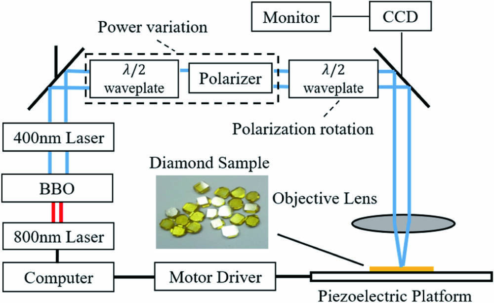
The experimental setup is shown in Fig. 1. A 400 nm femtosecond laser obtained by the second harmonic generation from a mode-locked Ti:sapphire ultrafast amplified laser (Spectral Physics, America; wavelength: 800 nm; pulse width: 100 fs; repetition rate: 1 kHz) was used. After passing through a shutter, the laser power was modulated with a half-wave plate and a polarizer. Subsequently, the laser passed through a half-wave plate, which was fixed in a hollow stepper motor to adjust the polarization direction dynamically. Finally, the laser passing through galvo mirrors and two lenses (4F system) was focused by a microscope object () on a diamond surface. The HPHT diamond with crystal orientation used in the experiment (the inset in Fig. 1) appears light yellow due to impurities and color centers. The samples were wiped with acetone and ethanol, followed by ultrasonic cleaning for 15 min in turn before laser scanning, and then placed on the piezoelectric ceramic plate of a six-axis manual stage to make adjustments of sample position and surface inclination. The piezoelectric ceramic platform could perform nano-scale adjustment in the direction. After laser scanning, the sample was ultrasonically cleaned with deionized water for 30 min in order to remove debris from the sample surface. After cleaning, the micro structures on the sample were characterized by scanning electron microscopy (SEM, JSM-7500F, JEOL).

Figure 1.Sketch diagram of femtosecond laser processing system.
The uniformity of the subwavelength structures induced by the femtosecond laser was closely related to the pulse energy. The stripes induced by low energy pulses were discontinuous, and there were no obvious cycles. High-energy pulses will change the local area and cannot form continuous regular stripe structures. Figure 2 shows the SEM images of micro-nano structures induced by different pulse energies with the same scanning direction and polarization laser. When the laser power is 2.50 μW, no obvious periodic stripe structures are observed, as shown in Fig. 2 (a). There are some tiny particles smaller than the width of stripes attached on the diamond surface. When the laser power is 2.76 μW, distinct stripe structures can be observed in Fig. 2(b). However, the structures have no obvious periodicity. When the laser power is up to 2.92 μW, the stripes are clearly visible, and the period of the structure is 100 nm, as shown in Fig. 2(c). When the laser power is 3.07 μW, the stripes become blurred and gradually lose periodicity in Fig. 2(d). Insets are the Fourier transform spectral patterns corresponding to stripe structures processed with different laser powers. From the spectrograms, it can be observed that the uniformity of stripes in Fig. 2(c) is significantly better than that of other structures processed with different pulse energies.
Figure 2.SEM images of stripe structures induced by different laser powers: (a) 2.50 μW, (b) 2.76 μW, (c) 2.92 μW, and (d) 3.07 μW; insets are the Fourier transform spectrum patterns corresponding to the stripes processed with different laser powers.
Line widths can be set by changing the scanning intervals in laser scanning. The direction of the induced stripes can be controlled by changing the polarization direction of the laser. The preparation of the micro-nano composite structures can be achieved by adjusting the scanning direction and the laser polarization direction. Figure 3 shows the SEM images of different scanning and polarization directions. The laser scanning direction is marked with yellow arrows, and the laser polarization direction is marked with red double arrows in Fig. 3. The directions of laser scanning and laser polarization are both in the horizontal direction in Fig. 3(a1). The stripes formed by laser scanning are in the horizontal direction, and the induced nano-stripes are in the vertical direction. A two-cycle structure perpendicular to each other is formed. In Fig. 3(b1), the laser scanning is in the vertical direction, and the laser polarization is in horizontal direction. A two-cycle structure with the same orientation is formed. In Fig. 3(c1), the laser scanning direction and laser polarization direction are at an angle of 45°. A double-cycle composite structure with an included angle of 45° is formed. The use of laser focus scanning for material removal and polarization-dependent nano-stripe induction enables the preparation of a single-pass uniform dual-cycle complex structure.
Figure 3.Two-cycle nano composite structures induced by different scanning directions and laser polarization directions: (a1) the scanning direction is the same as the polarization direction, (b1) the direction of scanning is perpendicular to the polarization direction, (c1) the angle between the directions of scanning and polarization is 45°; (a2)–(c2) are the corresponding magnification images of (a1)–(c1).
Then, the SERS characteristic[20] of the diamond nano-stripe structure was tested. Gold films with different thicknesses on the diamond surface nano-stripes were obtained by sputter-coating on the diamond surface. A pump laser with wavelength of 532 nm was used as the excitation line, and different concentrations of Rhodamine 6G (R6G) molecules were used as probes to carry out Raman measurements. In Fig. 4(a), the R6G molecules of were used as a probe, and 0 nm, 13 nm, 22 nm, 30 nm, 38 nm, 47 nm, and 55 nm thick gold films were sputtered. The Raman spectra show that the enhancement effect of the nano-stripe is the best when the gold film thickness is 47 nm. The peak is the characteristic Raman peak of diamond materials[21]. The peak near represents the existence of non-diamond carbon produced after laser processing of the diamond surface, whose reason is the in-plane stretching vibration of C-atom hybridization[22]. The Raman spectra of R6G molecules with different concentrations were measured by using the nano-stripe structure with 47-nm-thick gold film, as shown in Fig. 4(b). It can be seen that the intensity of Raman signal decreases with the decrease of R6G molecular concentration. The scattering peaks near are caused by the stretching vibration and bending vibration of the bond[23], and there are a lot of impurities and defects in the yellow diamond sample, which makes the photoluminescence background obvious.
Figure 4.Surface enhanced Raman scattering (SERS) measurements of the diamond surface nano-stripe structure: (a) the R6G molecules of were used as probes, and thicknesses of 0 nm, 13 nm, 22 nm, 30 nm, 38 nm, 47 nm, and 55 nm gold films were sputtered on the nano-stripes; (b) R6G molecules with different concentrations with 47-nm-thick gold film on nano-stripe structure.
The fixed scanning direction and polarization direction of the laser can only produce a uniform dual-cycle nanocomposite structure. However, the induced stripe direction can be controlled by dynamically adjusting the polarization direction of the laser during processing. Figure 5 shows the processing results of a single-line structure with horizontal scanning directions varying with different polarization directions. Figures 5(a)–5(c) correspond to the cases where the polarization directions are horizontal, vertical, and at an angle of 45° to the vertical. The direction of the induced stripes varies with position, and the entire line remains unchanged. The continuous change of the laser polarization direction within 8 mm scanning line was accomplished by adjusting the rotation speed of the stepping motor in Fig. 1, which was 0.47 rad/s, 0.94 rad/s, and 1.88 rad/s, in Figs. 5(d), 5(e), and 5(f), respectively. The direction of the stripes in Fig. 5(d) changes from vertical to horizontal. The direction of the stripes in Fig. 5(e) changes from vertical to horizontal and then to vertical, completing a 180° transition. The direction of the stripes in Fig. 5(f) undergoes a 360° (vertical-horizontal-vertical-horizontal-vertical) continuous transformation. By fixing the laser scanning direction and adjusting the polarization direction of the laser, continuously controllable change of the direction of the induced stripes in the track line trace can be achieved, which provides an effective reference for the preparation of complex micro-nano composite structures.
Figure 5.Control of the induced stripe direction in the scanning tracks by changing the polarization direction of the laser: (a) the scanning direction is the same as the polarization direction, (b) the direction of scanning is perpendicular to the direction of polarization, (c) the angle between the direction of scanning and the direction of polarization is 45°, and (d) the direction of polarization changes 90°, (e) the direction of polarization changes 180°, and (f) the direction of polarization changes 360°.
By controlling the laser scanning direction and the laser polarization direction simultaneously, a more complicated micro-nano composite structure can be prepared. Figures 6(a1) and 6(a2) show a circular structure prepared when the direction of laser polarization is in the fixed horizontal direction, and the direction of the nano-stripes in the ring is fixed in the vertical direction. Figures 6(b1), 6(b2), 6(c1), and 6(c2) show the micro-nano composite circular ring structures prepared by uniformly changing the polarization direction by 360°, in which the stripe direction is uniformly changed by 360°. In Figs. 6(b1) and 6(b2), the nano-stripes are located along the angular direction, and, in Figs. 6(c1) and 6(c2), the nano-stripes are along the radial direction. The differences between the nano-stripes and the scan path are determined by the laser polarization state and the initial phase of laser scanning, regardless of the speed of polarization change. The polarization directions in Figs. 6(d1), 6(d2), 6(e1), and 6(e2) have been changed by and , respectively. Figures 6(a2)–6(e2) show the relationship between the stripe direction and the relative position of the scan path. The rotation speed of the stepping motor in Fig. 6 is 2.62 rad/s in Figs. 6(b1) and 6(c1), 5.236 rad/s in Fig. 6(d1), and 7.854 rad/s in Fig. 6(e1).
Figure 6.Circular micro-nano composite structures were prepared when the laser scanning path and the polarization direction were changing at the same time: (a1), (a2) fixed polarization direction; (b1), (b2), (c1), (c2) change of polarization direction from the initial phase of ; (d1), (d2) change of polarization direction from the initial phase of ; (e1), (e2) change of polarization direction from the initial phase of .
Through the above-mentioned dynamic fine control of the laser polarization direction, laser power, and laser focus scanning speed, we have realized a variety of micro-nano composite structures on the surface of diamond materials. In the follow-up experiment, we will continue to explore the preparation of micro-nano structures and complex devices on the diamond surface, which will provide a powerful reference for processing micro-nano structures on diamond materials.
In conclusion, a 400 nm femtosecond laser was used to prepare a variety of micro-nano complex structures on the HPHT diamond surface. By dynamically adjusting the laser polarization direction during the scanning, a combination of patterns of micrometer-scale direct writing lines and nano-scale-induced stripes was prepared. The diamond micro-nano composite structures exhibited good SERS properties near with 47-nm-thick gold film. High-precision surface modification processing of super hard materials was demonstrated, which provides a new idea for further applications and three-dimensional modification of super-hard material surface.
References
[1] R. N. Patel, T. Schroeder, N. Wan, L. Li, S. L. Mouradian, E. H. Chen, D. R. Englund. Light-Sci. Appl., 5, e16032(2016).
[2] W. Chen, B. Liu, Y. Song, L. Chai, Q. Cui, Q. Liu, C. Wang, M. Hu. High Power Laser Sci. Eng., 6, e18(2018).
[3] L.-S. Fan, L. Constantin, D.-W. Li, L. Liu, K. Keramatnejad, C. Azina, X. Huang, H. R. Golgir, Y. Lu, Z. Ahmadi, F. Wang, J. Shield, B. Cui, J.-F. Silvain, Y.-F. Lu. Light-Sci. Appl., 7, 17177(2018).
[4] X.-F. Song, J.-J. Yang, H.-T. Ren, B. Lin, Y. Nakanishi, L. Yin. Int. J. Adv. Manuf. Technol., 96, 387(2018).
[5] H. Ni, Y. Wang, H. Gong, L. Pan, Z. J. Li, D. Wang. Int. J. Adv. Manuf. Technol., 95, 2185(2018).
[6] S. V. Gasilov, A. Mittone, T. dos Santos Rolo, S. Polyakov, S. Zholudev, S. A. Terentyev, V. Blank, A. Bravin, T. Baumbach. J. Synchrotron Radiat., 24, 1137(2017).
[7] Y. Zhang, Y. Li, L. Liu, C. Yang, Y. Chen, S. Yu. Opt. Express, 25, 15572(2017).
[8] X.-Q. Liu, Q.-D. Chen, K.-M. Guan, Z.-C. Ma, Y.-H. Yu, Q.-K. Li, Z.-N. Tian, H.-B. Sun. Laser Photon. Rev., 11, 1600115(2017).
[9] Y.-L. Sun, W.-F. Dong, L.-G. Niu, T. Jiang, D.-X. Liu, L. Zhang, Y.-S. Wang, Q.-D. Chen, D.-P. Kim, H.-B. Sun. Light-Sci. Appl., 3, e129(2014).
[10] F. Fraggelakis, E. Stratakis, P. A. Loukakos. Appl. Surf. Sci., 444, 154(2018).
[11] A. V. Bogatskaya, E. A. Volkova, A. M. Popov. Laser Phys. Lett., 15, 065301(2018).
[12] S. Dhomkar, P. R. Zangara, J. Henshaw, C. A. Meriles. Phys. Rev. Lett., 120, 117401(2018).
[13] Y.-C. Chen, P. S. Salter, S. Knauer, L. Weng, A. C. Frangeskou, C. J. Stephen, S. N. Ishmael, P. R. Dolan, S. Johnson, B. L. Green, G. W. Morley, M. E. Newton, J. G. Rarity, M. J. Booth, J. M. Smith. Nat. Photon., 11, 77(2017).
[14] L. Jiang, A.-D. Wang, B. Li, T.-H. Cui, Y.-F. Lu. Light-Sci. Appl., 7, 17134(2018).
[15] S. Gao, Z.-H. Wang, J.-G. Hua, Q.-K. Li, A.-W. Li, Y.-H. Yu. Acta Phys. Sin., 66, 147901(2017).
[16] J. Reif, O. Varlamova, S. Varlamov, M. Bestehorn. Appl. Phys. A Mater. Sci. Process., 104, 969(2011).
[17] C. Yao, W. Gao, Y. Ye, Y. Jiang, S. Xu, X. Yuan. Int. J. Modern Phys. B, 31, 1744004(2017).
[18] A. Abdelmalek, B. Sotillo, Z. Bedrane, V. Bharadwaj, S. Pietralunga, R. Ramponi, E. H. Amara, S. M. Eaton. AIP Adv., 7, 105105(2017).
[19] O. H. Y. Zalloum, M. Parrish, A. Terekhov, W. Hofmeister. Opt. Express, 18, 13122(2010).
[20] Y. Jiang, D.-W. Sun, H. Pu, Q. Wei. Trends Food Sci. Technol., 75, 10(2018).
[21] B. Sotillo, V. Bharadwaj, J. P. Hadden, M. Sakakura, A. Chiappini, T. T. Fernandez, S. Longhi, O. Jedrkiewicz, Y. Shimotsuma, L. Criante, R. Osellame, G. Galzerano, M. Ferrari, K. Miura, R. Ramponi, P. E. Barclay, S. M. Eaton. Sci. Rep., 6, 35566(2016).
[22] S. Gao, Z. Z. Li, Z. Y. Hu, F. Yu, Q. D. Chen, Z. N. Tian, H. B. Sun. Opt. Lett., 45, 2684(2020).
[23] A. C. Ferrari, J. Robertson. Phys. Rev. B, 63, 121405(2001).