
Lin Zhang, Jiamin Liu, Hao Jiang, Honggang Gu, Shiyuan Liu. Layer-dependent photoexcited carrier dynamics of WS2 observed using single pulse pump probe method[J]. Chinese Optics Letters, 2022, 20(10): 100002
- Chinese Optics Letters
- Vol. 20, Issue 10, 100002 (2022)
Abstract
1. Introduction
Transition metal dichalcogenides (TMDs) have attracted tremendous attention and played an important role in the development of two-dimensional (2D) semiconductor materials in the past decade due to their unique physical properties and outstanding photoelectric performance[
As one of the most studied materials in the family of TMDs, tungsten disulphide () has been widely used in the field of highly responsive photosensors and electrics devices. A deep understanding of the ultrafast carrier dynamics of and the corresponding mechanisms upon photoexcitation is the prerequisites for its applications. Therefore, many time-domain studies have been carried out on the photoexcited carrier dynamics of and utilizing transient absorption spectroscopy[
It is well known that, in the measurement of dynamic processes on ultrafast time scales, the reported methods include multi-shot methods[
Sign up for Chinese Optics Letters TOC. Get the latest issue of Chinese Optics Letters delivered right to you!Sign up now
2. Experiments
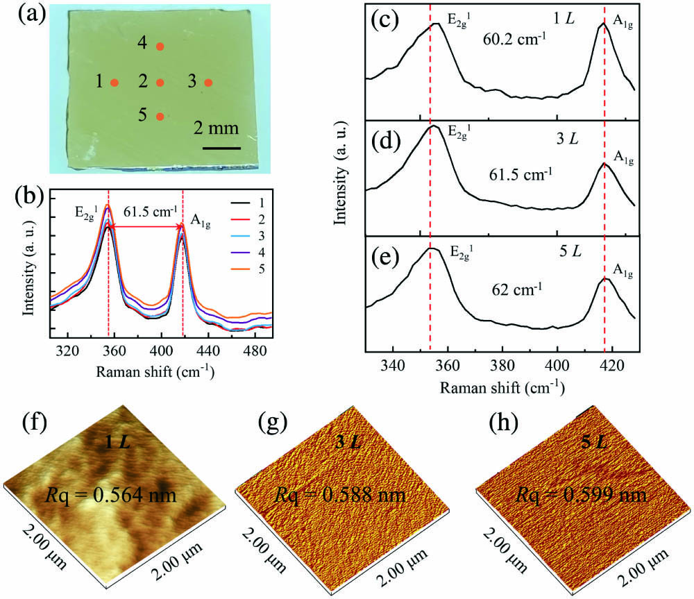
The samples were obtained through commercial purchase (6Carbon Technology), prepared using the chemical vapor deposition (CVD) method. The substrate is sapphire with a thickness of 0.3 mm. Figure 1(a) shows the optical image of the three-layer with size of . A Raman spectrometer (inVia Reflex) is used to analyze the Raman spectra, and the excitation wavelength is set as 532 nm. Figure 1(b) shows the Raman spectra at different marked positions, shown as Fig. 1(a). Two characteristic peaks ( and ) in the spectrum are observed, which represent two kinds of phonon vibration modes (in-plane and out-of-plane, respectively). The position differences between the two peaks maintain in five measurements, which means that the thickness uniformity of the sample is good. The Raman spectra of the from monolayer to five layers are shown in Figs. 1(c)–1(e), respectively. The position difference between peak and peak shows a dependence on the number of layers, which is consistent with previous reports[
![]()
Figure 1.Characterization of the WS2 films with different layers used in this study. (a) Optical image of sample with size of 10 mm × 10 mm. The WS2 film was plated on a 0.3 mm sapphire substrate by the CVD method. (b) Raman spectra of the three-layer WS2 at different points. (c)–(e) Raman spectra of WS2 films with 1–5 layers. (f)–(h) The surface roughness of the 1L, 3L, and 5L samples characterized by AFM.
The schematic diagram of the proposed single pulse pump probe method is shown in Fig. 2(a), which is similar to the configuration in our previous work[
![]()
Figure 2.(a) Schematic diagram of the pump-probe-based optical configuration. (b) Schematic diagram of the marked area in (a). The probe light spot size is smaller than the pump light spot and falls in the center of the pump light spot on the sample. NPBS, non-polarized beam splitter; P, polarizer; F, neutral filter wheel; M, mirror; S, mechanical shutter; L, lens.
3. Results and Discussion
The experiment of the photoexcited free carrier dynamics of is performed at room temperature. It is worth noting that the pulse energy fluctuation will introduce non-negligible measurement errors and even affect the observation of dynamic signals. However, such effects could be minimized by the single-shot strategy because all the data are collected in one test. Based on the above experimental conditions, Fig. 3(a) shows the measured static spectrum (without pump) and dynamic spectrum (with pump), where the wavelength dimension has been mapped into the time domain. It should be noted that the spectra shown in Fig. 3 are the results of the three-layer sample. Obviously, it can be seen that the transmitted light intensity of the probe beam drops rapidly at the moment of pump excitation, as marked in Fig. 3(a). The decrease in transmitted intensity may be due to the enhanced absorption of the probe light by the sample. Through differential processing, a spectrum containing the dynamic evolution information at the detecting area can be obtained as Fig. 3(b). The horizontal black dashed line represents , where . The open circles are the measured data, and the solid line represents the corresponding fitting result using a biexponential function, which can be described as
![]()
Figure 3.(a) Static spectrum I0 (black line) and dynamic spectrum I1 (blue line). The time of pump excitation is marked. (b) Spectrum after differential processing. The open circles are the measured data, and the solid line represents the corresponding fitting result using a biexponential function. The spectra shown in this figure are the results of the three-layer WS2 sample.
In order to further reveal the layer dependency of the dynamic response of being excited, the fs pump probe experiments were performed on samples with different numbers of layers. Figure 4 shows the temporal evolution of the transmitted light intensity extracted from the measured spectrum, where the layers are 1L, 3L, and 5L. Since the change of the probe light intensity is proportional to the carrier population changes[
![]()
Figure 4.Temporal evolution of the transmitted probe light intensity ΔI/I0 of the WS2 films with different layers (1L, 3L, and 5L). The open circles are extracted from the measured spectrum, and the solid lines are the results of fitting using a biexponential function.
Then, the layer dependency of the characteristic time for the three phases in the dynamic response of the carriers is discussed. First, the relationship between the fast carrier excitation time and the layers is shown in Fig. 5(a). It can be found that the carrier excitation time of monolayer () is significantly shorter than that of multilayer films (), and no obvious trend can be concluded. The characteristic times for decay processes ( and ) of with different layers that are extracted from the biexponential function fitting process are shown in Table 1. Correspondingly, Figs. 5(b) and 5(c) show the layer dependence of and . It can be observed that the fast decay phase is on the time scale from several picoseconds to tens of picoseconds, while the slow decay phase is in the scale of hundreds of picoseconds. The solid lines are the fitting results using an exponential function. Obviously, the characteristic time of the fast decay phase has an exponential decay trend with the layers. In contrast, the characteristic time of the slow decay phase increases exponentially as the number of layers increases.
| Parameters | Layers | ||
|---|---|---|---|
| 1L | 3L | 5L | |
| 20.9 | 8.4 | 3.9 | |
| 139.2 | 338.1 | 673.4 | |
Table 1. The Characteristic Times
![]()
Figure 5.(a) Characteristic time of the carrier excitation process as a function of the material layers. (b) The layer dependence of the carrier fast decay characteristic time and (c) the slow decay characteristic time in the process of carrier decay. The corresponding solid lines in (b) and (c) are the fitting results using an exponential function.
It is worth noting that the characteristic time of the carrier dynamic response (the rise and decay) obtained in our experiment is longer than the results reported in Refs. [18,21], which may be attributed to the relatively high pump pulse fluence used in our work[
We now discuss the mechanism that contributes to the observed phenomenon. First, we can start with the fast photoexcitation phase with characteristic time . The films absorb the photon energy, and the electrons transition from the valence band to the conduction band once the pump pulse irradiates on the sample surface. During this process, the carrier generation rate is much faster than the carrier recombination rate, and a large number of electrons and holes accumulate at the bottom of the conduction band and on the top of the valence band, respectively. The existence of these hot carriers inevitably makes the system partly in a non-equilibrium state. Therefore, these unstable electrons and holes need to release their own energy to balance the system. Next, we consider the mechanism of the fast decay phase of the hot carrier with characteristic time . Theoretical predictions of the radiative recombination time are on the nanosecond scale[
Further, we may try to explain the mechanism of the layer dependency of the characteristic time for the decay processes. It can be observed from Figs. 5(b) and 5(c) that the characteristic time of the fast decay phase decreases exponentially with the increase of the layer number. In other words, the carrier recombination rate increases as the number of layers increases. Conversely, the characteristic time of the slow recombination phase increases exponentially with the increase of the layer number. Such phenomena may be explained from the perspective of the photoexcited carrier numbers. As the number of layers increases, more carriers will be excited by the radiated pump pulse, which induce the increase of the carrier recombination rate. By the same token, the increase in the carrier number will take longer to pair the electron–hole and finally reach an equilibrium state.
4. Conclusion
In summary, a pump probe method has been proposed to study the ultrafast carrier dynamics of monolayer and few-layer excited by a fs pump pulse with fluence of . It has been demonstrated that with the configuration proposed in our work, the dynamics of the photoexcited carriers within 282 ps can be obtained. Moreover, the layer dependency of the characteristic time of carrier dynamics has been studied. Results show that the monolayer exhibits a unique photoexcitation time, while the layer dependency of the photoexcitation time for the multilayer material is not observed. The carrier recombination stage shows a strong layer dependency. In addition, Auger recombination is considered to be the main mechanism of carrier recombination. The proposed method in this work is expected to be an effective approach to explore the ultrafast dynamics of photoexcited carriers in 2D semiconductor materials. This work also provides a further understanding of the mechanism of the photoexcited carrier dynamics of layered , which is the prerequisite for applying TMDs in the field of photoelectronic and photovoltaic devices.
References
[1] C. Cong, J. Shang, Y. Wang, T. Yu. Optical properties of 2D semiconductor WS2. Adv. Opt. Mater., 6, 1700767(2018).
[2] R. K. Chowdhury, S. Nandy, S. Bhattacharya, M. Karmakar, S. N. B. Bhaktha, P. K. Datta, A. Taraphder, S. K. Ray. Ultrafast time-resolved investigations of excitons and biexcitons at room temperature in layered WS2. 2D Mater., 6, 015011(2018).
[3] T. Zhu, J. M. Snaider, L. Yuan, L. Huang. Ultrafast dynamic microscopy of carrier and exciton transport. Annu. Rev. Phys. Chem., 70, 219(2019).
[4] K. S. Novoselov, D. Jiang, F. Schedin, T. J. Booth, V. V. Khotkevich, S. V. Morozov, A. K. Geim. Two-dimensional atomic crystals. Proc. Natl. Acad. Sci. USA, 102, 10451(2005).
[5] H. Gu, B. Song, M. Fang, Y. Hong, X. Chen, H. Jiang, W. Ren, S. Liu. Layer-dependent dielectric and optical properties of centimeter-scale 2D WSe2: evolution from a single layer to few layers. Nanoscale, 11, 22762(2019).
[6] B. Song, H. Gu, M. Fang, Y.-T. Ho, X. Chen, H. Jiang, S. Liu. Complex optical conductivity of 2D MoS2: a striking layer-dependency. J. Phys. Chem. Lett., 10, 6246(2019).
[7] K. F. Mak, C. Lee, J. Hone, J. Shan, T. F. Heinz. Atomically thin MoS2: a new direct-gap semiconductor. Phys. Rev. Lett., 105, 136805(2010).
[8] L. Gao. Flexible device applications of 2D semiconductors. Small, 13, 1603994(2017).
[9] D. Jariwala, V. K. Sangwa, L. J. Lauhon, T. J. Marks, M. C. Hersam. Emerging device applications for semiconducting two-dimensional transition metal dichalcogenides. ACS Nano, 8, 1102(2014).
[10] B. W. Baugher, H. O. Churchill, Y. Yang, P. Jarillo-Herrero. Optoelectronic devices based on electrically tunable p-n diodes in a monolayer dichalcogenide. Nat. Nanotechnol., 9, 262(2014).
[11] T. Yang, H. Lin, B. Jia. Ultrafast direct laser writing of 2D materials for multifunctional photonics devices [Invited]. Chin. Opt. Lett., 18, 023601(2020).
[12] T. Jiang, R. Chen, X. Zheng, Z. Xu, Y. Tang. Photo-induced excitonic structure renormalization and broadband absorption in monolayer tungsten disulphide. Opt. Express, 26, 859(2018).
[13] P. Schiettecatte, P. Geiregat, Z. Hens. Ultrafast carrier dynamics in few-layer colloidal molybdenum disulfide probed by broadband transient absorption spectroscopy. J. Phys. Chem. C, 123, 10571(2019).
[14] Y. Li, W. Liu, Y. Wang, Z. Xue, Y. C. Leng, A. Hu, H. Yang, P. H. Tan, Y. Liu, H. Misawa, Q. Sun, Y. Gao, X. Hu, Q. Gong. Ultrafast electron cooling and decay in monolayer WS2 revealed by time- and energy-resolved photoemission electron microscopy. Nano Lett., 20, 3747(2020).
[15] A. Hu, W. Liu, X. Li, S. Xu, Y. Li, Z. Xue, J. Tang, L. Ye, H. Yang, M. Li, Y. Ye, Q. Sun, Q. Gong, G. Lu. Spectromicroscopy and imaging of photoexcited electron dynamics at in-plane silicon pn junctions. Nanoscale, 13, 2626(2021).
[16] W. Zheng, P. Jiang, L. Zhang, Y. Wang, Q. Sun, Y. Liu, Q. Gong, C. Wu. Ultrafast extreme ultraviolet photoemission electron microscope. Rev. Sci. Instrum., 92, 043709(2021).
[17] L. Yuan, L. Huang. Exciton dynamics and annihilation in WS2 2D semiconductors. Nanoscale, 7, 7402(2015).
[18] X. Xing, L. Zhao, Z. Zhang, X. Liu, K. Zhang, Y. Yu, X. Lin, H. Y. Chen, J. Q. Chen, Z. Jin, J. Xu, G.-h. Ma. Role of photoinduced exciton in the transient terahertz conductivity of few-layer WS2 laminate. J. Phys. Chem. C, 121, 20451(2017).
[19] J. K. Gustafson, P. D. Cunningham, K. M. McCreary, B. T. Jonker, L. M. Hayden. Ultrafast carrier dynamics of monolayer WS2 via broad-band time-resolved terahertz spectroscopy. J. Phys. Chem. C, 123, 30676(2019).
[20] H. Wang, C. Zhang, F. Rana. Ultrafast dynamics of defect-assisted electron-hole recombination in monolayer MoS2. Nano Lett., 15, 339(2015).
[21] C. Ruppert, A. Chernikov, H. M. Hill, A. F. Rigosi, T. F. Heinz. The role of electronic and phononic excitation in the optical response of monolayer WS2 after ultrafast excitation. Nano Lett., 17, 644(2017).
[22] Z. Chi, H. Chen, Q. Zhao, Y. X. Weng. Observation of the hot-phonon effect in monolayer MoS2. Nanotechnology, 31, 235712(2020).
[23] Z. Nie, R. Long, L. Sun, C. C. Huang, J. Zhang, Q. Xiong, D. W. Hewak, Z. Shen, O. V. Prezhdo, Z. H. Loh. Ultrafast carrier thermalization and cooling dynamics in few-layer MoS2. ACS Nano, 8, 10931(2014).
[24] V. Vega-Mayoral, D. Vella, T. Borzda, M. Prijatelj, I. Tempra, E. A. Pogna, S. Dal Conte, P. Topolovsek, N. Vujicic, G. Cerullo, D. Mihailovic, C. Gadermaier. Exciton and charge carrier dynamics in few-layer WS2. Nanoscale, 8, 5428(2016).
[25] Z. E. Eroglu, O. Comegys, L. S. Quintanar, N. Azam, S. Elafandi, M. Mahjouri-Samani, A. Boulesbaa. Ultrafast dynamics of exciton formation and decay in two-dimensional tungsten disulfide (2D-WS2) monolayers. Phys. Chem. Chem. Phys., 22, 17385(2020).
[26] A. Brasington, D. Golla, A. Dave, B. Chen, S. Tongay, J. Schaibley, B. J. LeRoy, A. Sandhu. Role of defects and phonons in bandgap dynamics of monolayer WS2 at high carrier densities. J. Phys. Mater., 4, 015005(2021).
[27] P. D. Cunningham, K. M. McCreary, A. T. Hanbicki, M. Currie, B. T. Jonker, L. M. Hayden. Charge trapping and exciton dynamics in large-area CVD grown MoS2. J. Phys. Chem. C, 120, 5819(2016).
[28] Y. Zhao, Q. Huang, H. Cai, X. Lin, H. He, H. Cheng, T. Ma, Y. Lu. Ultrafast control of slow light in THz electromagnetically induced transparency metasurfaces. Chin. Opt. Lett., 19, 073602(2021).
[29] L. Zhang, J. Liu, W. Gong, H. Jiang, S. Liu. Diffraction based single pulse measurement of air ionization dynamics induced by femtosecond laser. Opt. Express, 29, 18601(2021).
[30] Q. Yue, Z. Cheng, L. Han, Y. Yang, C. Guo. One-shot time-resolved holographic polarization microscopy for imaging laser-induced ultrafast phenomena. Opt. Express, 25, 14182(2017).
[31] Z. Zhong, L. Zhang, H. Jiang, W. Gong, H. Gu, X. Chen, S. Liu. A Brewster incidence method for shocked dynamic metrology of transparent materials and its error evaluation. AIP Adv., 10, 105203(2020).
[32] H. Tsai, Y. Huang, P. Tsai, Y. Chen, H. Ahn, S. Lin, Y. Lu. Ultrafast exciton dynamics in scalable monolayer MoS2 synthesized by metal sulfurization. ACS Omega, 5, 10725(2020).
[33] Z. Zhong, W. Gong, H. Jiang, H. Gu, X. Chen, S. Liu. Investigation of spatial chirp induced by misalignments in a parallel grating pair pulse stretcher. Appl. Sci., 10, 103110(2020).
[34] M. Palummo, M. Bernardi, J. C. Grossman. Exciton radiative lifetimes in two-dimensional transition metal dichalcogenides. Nano Lett., 15, 2794(2015).
[35] H. Wang, C. Zhang, W. Chan, C. Manolatou, S. Tiwari, F. Rana. Radiative lifetimes of excitons and trions in monolayers of the metal dichalcogenide MoS2. Phys. Rev. B, 93, 045407(2016).

Set citation alerts for the article
Please enter your email address
© Copyright 2018-2021 | Chinese Laser Press. All Rights Reserved 沪ICP备15018463号-20