
Hanmeng Li, Xingjian Xiao, Bin Fang, Shenglun Gao, Zhizhang Wang, Chen Chen, Yunwei Zhao, Shining Zhu, Tao Li. Bandpass-filter-integrated multiwavelength achromatic metalens[J]. Photonics Research, 2021, 9(7): 1384
- Photonics Research
- Vol. 9, Issue 7, 1384 (2021)
Abstract
1. INTRODUCTION
Metasurfaces with flexible control of the amplitude, phase, and polarization of light by subwavelength nanostructures have been introduced and widely developed [1–4]. Based on the potential to control and manipulate the flow of light, a large number of metasurfaces have been proposed recently as alternatives to conventional optical elements, promoting the miniaturization and function expansion of the device. In addition to various potential applications of metasurfaces, such as holograms [5,6], wave plates [7,8], beam shapers [9,10], and optical switches [11,12], metalenses have attracted intense interest in the last few years due to their wide applications in both consumer and industry products [13–16]. Great efforts have been made toward improving the performance of the metalens, especially the chromatic aberration correction [17–28].
Although the chromatic aberration of metalenses is alleviated to a certain extent, the design of large-scale, high-numerical-aperture, and broadband achromatic flat lenses is still a bottleneck of imaging technology and remains a big challenge in metalens design. In recent works [23,29], it was found that the major reason is that there are some intrinsic constraints among these parameters. The results reveal that the efficiency of the metalens has a negative correlation with the numerical aperture and achromatic bandwidth. By reducing the bandwidth or the number of wavelengths properly, the efficiency would possibly be improved. In fact, a color filter array (CFA) is widely applied to a monochromatic imager, especially the Bayer pattern in single-sensor color imaging systems [30], which means a discrete multiwavelength achromatism in the red, green, and blue (RGB) regions in the visible spectrum is much more practical and important to design the metalens. Some multiwavelength achromatic metasurfaces have been demonstrated toward this purpose [17,19]. However, these devices still suffer from low efficiency and serious crosstalk from the unmodulated wavelengths in the band under a natural white light illumination.
Here we propose a conceptually simple yet powerful approach for an RGB-3-band achromatic metalens with the incorporation of a well-designed bandpass filter, which can directly work under a broadband visible light. First we use a searching optimization algorithm to design a metalens with a numerical aperture (NA) of 0.2, which is achromatic at , 540, and 490 nm. The metalens exhibits a high focusing efficiency using the nanopillars and their Babinet hollow structures (inverse type). Besides the efficiency enhancement of the metalens, we introduce the design of the stacked multilayered bandpass filter, which is composed of multiple distributed Bragg reflectors (DBRs) and defect dielectric layers sandwiched between them fabricated of and to form the Fabry–Perot (FP) resonances at the RGB wavelengths [31,32]. The dependence of the FP resonances on the parameters of the defect layers provides free control over the spectral response of the bandpass filter. We show that by combining the bandpass filter and an accordingly proper metalens, it is able to realize the multiwavelength achromatism and minimize crosstalk from the other wavelengths simultaneously in the visible region. With this approach, the transmittance and the phase response of the device can be controlled independently and are shown to be compatible in manufacturing.
Sign up for Photonics Research TOC. Get the latest issue of Photonics Research delivered right to you!Sign up now
2. DESIGN OF THE METALENS
First we introduce our design process for the multiwavelength achromatic metalens. The primary goal is to find the proper structure pattern and arrangement of the meta-unit cells, which can realize the multiwavelength achromatic function. We applied the pattern search method named the Hooke–Jeeves (HJ) algorithm [33] to achieve this goal. The specific process of the HJ algorithm is shown in Fig. 1(a), where is the objective function or figure of merit (FoM), is the initial distribution, is the ultimate distribution after optimization, is the intermediate variable, is the acceleration factor, is the step size (which is an integer), and is the basis vector of which the th component is 1 with other components equal to 0 [i.e., ]. Briefly speaking, in the th epoch, the th element of will increase and decrease to get two new FoMs. If one of these new FoMs is better than the old one, the corresponding change in will go into effect. Here we selected to be the material of the metalens, considering its relatively high index of refraction and low loss in the visible light band, as well as its practical manufacturing compatibility. By employing a commercial software (Lumerical FDTD Solutions), we can obtain the response electrical field of different unit structures. We added 12 kinds of meta-units with a period of 350 nm including square, rectangular, circular, elliptical, toroidal, and cross-shaped pillars; the rest are the corresponding hollow structures (inverse type) of different geometries into our library as shown in Fig. 1(b). Each type of unit structure has only one or two geometry parameters (such as side length of the square, length and width of the rectangle, inner and outer diameters of the annulus; the cross can be treated as the combination of two rectangles); these parameters are designed in the range of 50 to 310 nm after calculation. The height of the meta-units is set to be 1 μm to get a high diffraction efficiency after careful optimizations. By encoding all the unit structures into number ( is the number of all structures with different parameters, which equals 6000 in our case), we can get an matrix . The element represents the electrical field of the th structure of the th frequency. According to the radial symmetry of the lens, we only need to calculate the radial structure distribution in lattices. Therefore, in each lattice, we have unit structures for selection. In our algorithm, the step size is a variable, which ranges from 1 to . The initial value of is set as 512, which is determined by the simulation results.
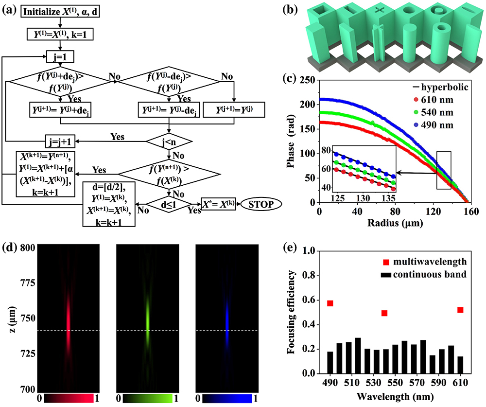
Figure 1.(a) Flow chart of the Hooke–Jeeves (HJ) algorithm used to design our metalens. (b) The schematics of 12 kinds of meta-unit architectures, including nanopillars and their Babinet hollow structures. Our designed metalens is composed of these meta-units with varying in-plane geometrical parameters. (c) The comparison of the standard hyperbolic phase profile (black lines) and the calculated ones of metalens at the designed wavelengths: 610 nm (red dots), 540 nm (green dots), 490 nm (blue dots). The inset is a zoom-in image for clarification. (d) Simulated focusing intensity distributions of the designed multiwavelength achromatic metalens, which is designed with an
In our calculations, we choose the electric-field intensity at the focal point as the single frequency FOM [34], which can be written as and can be calculated as follows:
Because there are three frequencies in our case, the problem is actually a multi-objective problem. In this case, based on maximum formulation [35], the whole FOM can be written as
Finally, the whole optimization problem can be converted to solve
Using the optimization approach mentioned above, we propose a multiwavelength achromatic metalens with a diameter of 300 μm and NA of 0.2, working at three designed spectral RGB components of 610, 540, and 490 nm. After completing all the calculations, we get the optimization result of the phase profile of the multiwavelength achromatic metalens at the designed wavelengths: 610 nm (red dots), 540 nm (green dots), and 490 nm (blue dots), which are consistent with the standard hyperbolic phase profile (black lines) as displayed in Fig. 1(c).
According to our calculation data, approximately 80% of the selected meta-units to combine our metalens are the structures symmetric in two arbitrary orthogonal directions in a plane showing polarization independence. As a result, the metalens is insensitive to the polarization state in general. Moreover, the phase response of the meta-units arises from the optical path in our case, which means the diffraction light keeps the original polarization state.
3. FOCUSING PROPERTIES OF THE METALENS
To characterize the focusing properties of the multiwavelength achromatic metalens, we use Lumerical FDTD Solutions for the full-wave simulations. The metalens diameter is set as 300 μm, and the NA is 0.2 given maintaining consistency with the calculated results, while the focal length is 735 μm theoretically for the three wavelengths. The normalized intensities in the simulation at the three wavelengths along the propagation direction ( axis) are shown in Fig. 1(d) for incident light at 610, 540, and 490 nm, respectively. As the white dashed lines at in Fig. 1(d) indicate, the metalens obtains an approximate focal distance of 735 μm, which means that we designed a multiwavelength achromatic metalens at three wavelengths (RGB) that are in good agreement with the calculation values. The focusing efficiency (the ratio of the intensity of the cross-sectional region of a diameter of 3 times the full width at half-maximum centered at the focal spot to the intensity that goes through the metalens [36,37]) was calculated, which is revealed in Fig. 1(d) for each wavelength, and found to be about 55%. For comparison, we use the same design optimization method to achieve a quasicontinuous band achromatic metalens. We divided the band (from 490 to 610 nm wavelength) into 15 wavelengths and satisfy simultaneously the achromatism for all these 15 wavelengths. An obvious decrease in the focusing efficiency at desired RGB 3-waveglengths can be found in Fig. 1(e), which is at the level of 22% because of the trade-off between the number of wavelengths and the focusing efficiency.
4. RGB-3-CHANNEL BANDPASS FILTER
As mentioned above, we need to realize a multiwavelength achromatic metalens with achromatic focusing for RGB lights, and the bandpass filter is designed for RGB channels accordingly. Here we demonstrate an RGB-3-channel bandpass filter composed of defect dielectric layers sandwiched between multiple DBRs. Every two groups of DBRs form an FP resonator whose center wavelength is controlled by the design of the defect dielectric layers. To design the FP bandpass filters, we use FDTD simulations to optimize the parameters of the DBRs and the defect dielectric layers by analyzing the transmission spectra of the whole structure. First, we need to define the basic configuration of our designed structure. To simplify the description, basic layers of () and () are symbolized as an H layer and the L layer, respectively. To meet the requirements of the filter in the visible region, the thickness of the H layer is set to 45 nm and the L layer is 62 nm accordingly. We use DBRs as the high-reflectivity mirrors forming the FP resonator. A basic DBR consists of four pairs of and quarter-wavelength stacks, represented by , whose subscript indicates the number of pairs. In order to form a stop band covering the whole 300 nm bandwidth (from 400 to 700 nm), we use multiple DBRs of different thicknesses to stack up and down. After the parameter optimization of the DBRs, we choose six DBRs to combine the whole band-stop filter represented by , and the orders of the DBRs indicate the actual structure from bottom to top. The numbers before H and L represent the coefficients that the thickness of each layer of the DBR should multiply.
In order to fulfill an RGB-3-channel bandpass filter, we introduce several defect layers between the DBRs to build cavities. The FP resonances are formed inside the cavities, which allow multiple Lorentzian-shaped peaks in the transmission spectrum. For this work, we choose two groups of defect layers to form three resonances within the DBRs’ stop band. We insert one group of () between the third and fourth DBRs and another group of () between the fourth and fifth DBRs. The six parameters (from to ) also indicate the coefficients that the thickness of each defect layer should multiply. The schematic of the filter is displayed in Fig. 2(a). The first group of defect layers contributes to the resonance in the blue band, while the second one mainly controls the two resonances in the green and red bands. In Fig. 2(b), the simulated transmission spectra varied with the critical parameter are plotted. We set the parameters from to , except , as 1.7, 2.65, 3.2, 4.5, and 4.1. The is treated as a variable, and we sweep it from 1.5 to 5.5 to get the optimal spectrum. When , the three peaks of transmittance, which are 99.6% (, red region, ), 97.5% (, green region, ), and 98.8% (, blue region, ), are achieved as shown by the black dashed line in Fig. 2(c).
![]()
Figure 2.(a) Schematic illustration of the proposed bandpass filter, which is composed of multiple DBRs and several dielectric defect layers sandwiched between them. (b) Simulated transmission spectrum of the designed filter varied with the parameter
As a proof of concept, the designed bandpass filter was fabricated on a single fused silica substrate. The and stacked layers are deposited by plasma-enhanced chemical vapor deposition (PECVD) in a predetermined sequence. We use a full-spectrum microspectro-photometer (CRAIC 20/30PV) to measure the transmission spectra of our samples. The purple solid line in Fig. 2(c) shows our experimental result, which agrees well with the simulation. The discrepancies in the blue and green light region probably come from the material absorption and small fabrication discrepancies.
After we fabricated the metalens ( and ) on top of our filter (the fabrication will be addressed in Section 5), we measured the transmission spectra of the complete sample in the same way as displayed by the red line in Fig. 2(c). The transmittance of the whole structure shows a slight drop due to the impact of the metalens. Finally, we obtain an expected spectrum of our complete device, exhibiting three peaks at the designed wavelengths, which are 71% (, red region, ), 59% (, green region, ), and 51% (, blue region, ), while the background transmittance in the 300 nm wavelength band is very low.
5. MEASUREMENT OF THE BANDPASS-FILTER-INTEGRATED MULTIWAVELENGTH ACHROMATIC METALENS
The fabrication of the multiwavelength achromatic metalens will be introduced here. First, the silicon nitride layer was deposited on the top of the bandpass filter using the PECVD to a final thickness of 1 μm. Then a 200 nm PMMA resist film was spin coated onto the sample and baked at 170°C for 5 min. Next, a 40 nm thick layer of water-soluble conductive polymer (AR-PC 5090) was spin coated on the resist for the dissipation of E-beam charges. The lens pattern was written on an electron beam resist using an E-beam writer (Elionix, ELS-F125). The conductive polymer was then dissolved in water, and the resist was developed in a resist developer solution. An electron beam evaporated chromium layer was used to reverse the generated pattern with a lift-off process and was then used as a hard mask for dry etching the silicon nitride layer. The dry etching was performed in a mixture of CHF3 and SF6 plasmas using an inductively coupled plasma reactive ion etching process (Oxford Instruments, PlasmaPro100 Cobra300). Finally, the chromium layer was removed by the stripping solution. Figure 3(a) shows the optical image of the whole metalens and scanning electron microscope (SEM) image of the selected part of the metalens.
![]()
Figure 3.(a) Optical image of the fabricated achromatic metalens with 0.2 NA and 300 μm diameter (scale bar is 50 μm) and the zoom-in SEM image shown in the right panel (scale bar is 1 μm). (b) Experimental longitudinal cross sections of the focusing light intensity by the filter-integrated multiwavelength achromatic metalens under additional filtered illuminations (10 nm bandwidth) at 610 nm (red region), 540 nm (green region), and 490 nm (blue region) wavelengths, respectively, above which is the normalized focal spots at the designed focal length of 735 μm.
The optical performance of the bandpass-filter-integrated multiwavelength achromatic metalens was measured via our homemade optical setup. First, the achromatism at the three wavelengths of the whole structure was demonstrated as it was illuminated by a white light laser (Fianium Super-continuum, 4 W) with a wavelength ranging from 450 to 660 nm. A linear polarizer (LP) was employed to generate a linear polarization incidence. To capture the light intensity profile, an achromatic objective () and a coupled charge device (CCD) were placed on a motorized stage and moved together along the propagation direction. The measured intensities of the focusing light at the three wavelengths (610, 540, and 490 nm) along the propagation direction ( axis) are displayed in Fig. 3(b) from left to right, respectively. Filters with a bandwidth of 10 nm are used to characterize the features at the three wavelengths. It is observed that at the designed focal length (the white dashed line at ) light is focused quite well at the designed wavelengths, showing a good multiwavelength achromatism. The normalized focal spots can be seen in the upper row of Fig. 3(b). The experimental focusing efficiencies for the three wavelengths (, 540, and 490 nm) reached 50%, 48%, and 47%, while the measured FWHMs are 1.81, 1.6, and 1.42 μm, respectively. For further analysis, we show the comparison of the normalized focusing intensity profile of the simulated and experimental results in Fig. 3(c). We also calculated the Strehl ratios of the experiment results (0.89 at 610 nm, 0.91 at 540 nm, and 0.78 at 490 nm) as shown in the panels.
Next, the 1951 United States Air Force (USAF) resolution test chart was employed to test the imaging performance of our imaging device. Instead of the super-continuous laser, a halogen light (incoherent) source is used to avoid speckle noises, and additional 10 nm bandwidth filters are used in the imaging processes to check its performance at individual wavelengths. The sample was directly mounted at twice the focal length in front of the metalens, corresponding to an optical system without the image zoom (here, ). Figures 4(a)–4(c) show the microscopic images of the USAF resolution test chart with filters of , 540, and 490 nm in turn, manifesting clear resolution of Element 1 and Group 8 (i.e., a resolution of 1.95 μm) without image change.
![]()
Figure 4.(a)–(c) Imaging results with the filter-integrated multiwavelength achromatic metalens under additional filtered illuminations (10 nm bandwidth) at 610 nm (red region), 540 nm (green region), and 490 nm (blue region) wavelengths, respectively. (d) and (e) The experiment captured white light images (without additional filters) for the cases of the filter-integrated multiwavelength achromatic metalens and that without the bandpass filter, respectively. The imaging target is a standard USAF resolution chart.
Afterwards, we removed the additional 10 nm filters to illuminate the resolution test chart with the white light and imaged it directly by bandpass-filter-integrated metalens, as shown by the results in Fig. 4(d). As expected, our device acquires a high white imaging quality, and especially the signal-to-noise ratio (SNR) is still high by eliminating crosstalk from other wavelengths. The chromatic aberration almost disappears, and the resolution remains at the level of 2 μm. To demonstrate the advantage of our device, we fabricated another sample of the same multiwavelength achromatic metalens on a bare fused silica substrate without the designed bandpass filter. Figure 4(e) shows its white light imaging of the resolution test chart that reveals quite low SNR. Since there is no filter to block other wavelengths, this image has strong chromatic aberrations, which greatly reduces the resolution (even Group 7 is indistinct) and degrades the imaging performance. To confirm the impact of the designed bandpass filter in our device, we measured the focusing performance of the two devices. Figures 4(f) and 4(g) show the longitudinal cross section of the focusing light intensity by the bandpass-filter-integrated metalens and that without the filter, respectively, with the super-continuum white light laser incidence. It is evident that our bandpass filter is greatly conductive to reduce the chromatic aberration in both the transverse and longitudinal directions around the focal spot as the white dashed lines (at ) in Figs. 4(f) and 4(g) reveal. The complete device exhibits greatly improved focusing capability for a white light incidence, which verifies the contrast of Figs. 4(d) and 4(e). Moreover, our approach provides the foundation for such ideas and is much more convenient in fabrication.
6. CONCLUSION
In summary, we have proposed and experimentally demonstrated a multiwavelength achromatic metalens integrating an RGB-3-channel bandpass filter. The metalens () is composed of nanopillars, and its inverse structures were designed using the searching optimization algorithm for RGB achromatism (, 540, and 490 nm) with high focusing efficiency. The spectrum of the bandpass filter can be flexibly controlled by changing the thicknesses of the defect dielectric layers inserted between the DBRs, which can be easily modulated to show three transmission peaks for the corresponding three wavelengths. The combination of the metalens and the filter not only greatly improves the imaging performance but also enriches the function expansion in designing metasurfaces for both the wavefront and spectrum manipulation simultaneously.
Acknowledgment
Acknowledgment. T. Li is grateful for the support from the Dengfeng Project B of Nanjing University.
References
[1] N. F. Yu, P. Genevet, M. A. Kats, F. Aieta, J. P. Tetienne, F. Capasso, Z. Gaburro. Light propagation with phase discontinuities: generalized laws of reflection and refraction. Science, 334, 333-337(2011).
[2] S. Sun, K.-Y. Yang, C.-M. Wang, T.-K. Juan, W. T. Chen, C. Y. Liao, Q. He, S. Xiao, W.-T. Kung, G.-Y. Guo, L. Zhou, D. P. Tsai. High-efficiency broadband anomalous reflection by gradient meta-surfaces. Nano Lett., 12, 6223-6229(2012).
[3] A. V. Kildishev, A. Boltasseva, V. M. Shalaev. Planar photonics with metasurfaces. Science, 339, 1232009(2013).
[4] N. Yu, F. Capasso. Flat optics with designer metasurfaces. Nat. Mater., 13, 139-150(2014).
[5] J. Lin, P. Genevet, M. A. Kats, N. Antoniou, F. Capasso. Nanostructured holograms for broadband manipulation of vector beams. Nano Lett., 13, 4269-4274(2013).
[6] Y.-W. Huang, W. T. Chen, W.-Y. Tsai, P. C. Wu, C.-M. Wang, G. Sun, D. P. Tsai. Aluminum plasmonic multicolor meta-hologram. Nano Lett., 15, 3122-3127(2015).
[7] N. Yu, F. Aieta, P. Genevet, M. A. Kats, Z. Gaburro, F. Capasso. A broadband, background-free quarter-wave plate based on plasmonic metasurfaces. Nano Lett., 12, 6328-6333(2012).
[8] F. Ding, Z. Wang, S. He, V. M. Shalaev, A. V. Kildishev. Broadband high-efficiency half-wave plate: a supercell-based plasmonic metasurface approach. ACS Nano, 9, 4111-4119(2015).
[9] L. Huang, X. Chen, H. Muehlenbernd, G. Li, B. Bai, Q. Tan, G. Jin, T. Zentgraf, S. Zhang. Dispersionless phase discontinuities for controlling light propagation. Nano Lett., 12, 5750-5755(2012).
[10] O. Avayu, O. Eisenbach, R. Ditcovski, T. Ellenbogen. Optical metasurfaces for polarization-controlled beam shaping. Opt. Lett., 39, 3892-3895(2014).
[11] D. Wen, F. Yue, G. Li, G. Zheng, K. Chan, S. Chen, M. Chen, K. F. Li, P. W. H. Wong, K. W. Cheah, E. Y. B. Pun, S. Zhang, X. Chen. Helicity multiplexed broadband metasurface holograms. Nat. Commun., 6, 8241(2015).
[12] E. Maguid, I. Yulevich, D. Veksler, V. Kleiner, M. L. Brongersma, E. Hasman. Photonic spin-controlled multifunctional shared-aperture antenna array. Science, 352, 1202-1206(2016).
[13] M. Khorasaninejad, W. T. Chen, R. C. Devlin, J. Oh, A. Y. Zhu, F. Capasso. Metalenses at visible wavelengths: diffraction-limited focusing and subwavelength resolution imaging. Science, 352, 1190-1194(2016).
[14] Z. B. Fan, Z. K. Shao, M. Y. Xie, X. N. Pang, W. S. Ruan, F. L. Zhao, Y. J. Chen, S. Y. Yu, J. W. Dong. Silicon nitride metalenses for close-to-one numerical aperture and wide-angle visible imaging. Phys. Rev. Appl., 10, 014005(2018).
[15] T. Li. New opportunities for metalenses in imaging applications. Sci. China Phys. Mech. Astron., 63, 284231(2020).
[16] G. Y. Lee, J. Y. Hong, S. Hwang, S. Moon, H. Kang, S. Jeon, H. Kim, J. H. Jeong, B. Lee. Metasurface eyepiece for augmented reality. Nat. Commun., 9, 4562(2018).
[17] B. Wang, F. L. Dong, Q. T. Li, D. Yang, C. W. Sun, J. J. Chen, Z. W. Song, L. H. Xu, W. G. Chu, Y. F. Xiao, Q. H. Gong, Y. Li. Visible-frequency dielectric metasurfaces for multiwavelength achromatic and highly dispersive holograms. Nano Lett., 16, 5235-5240(2016).
[18] E. Arbabi, A. Arbabi, S. M. Kamali, Y. Horie, A. Faraon. Controlling the sign of chromatic dispersion in diffractive optics with dielectric metasurfaces. Optica, 4, 625-632(2017).
[19] O. Avayu, E. Almeida, Y. Prior, T. Ellenbogen. Composite functional metasurfaces for multispectral achromatic optics. Nat. Commun., 8, 14992(2017).
[20] M. Khorasaninejad, Z. Shi, A. Y. Zhu, W. T. Chen, V. Sanjeev, A. Zaidi, F. Capasso. Achromatic metalens over 60 nm bandwidth in the visible and metalens with reverse chromatic dispersion. Nano Lett., 17, 1819-1824(2017).
[21] S. Wang, P. C. Wu, V.-C. Su, Y.-C. Lai, C. H. Chu, J.-W. Chen, S.-H. Lu, J. Chen, B. Xu, C.-H. Kuan, T. Li, S. Zhu, D. P. Tsai. Broadband achromatic optical metasurface devices. Nat. Commun., 8, 187(2017).
[22] W. T. Chen, A. Y. Zhu, V. Sanjeev, M. Khorasaninejad, Z. Shi, E. Lee, F. Capasso. A broadband achromatic metalens for focusing and imaging in the visible. Nat. Nanotechnol., 13, 220-226(2018).
[23] S. Shrestha, A. C. Overvig, M. Lu, A. Stein, N. F. Yu. Broadband achromatic dielectric metalenses. Light Sci. Appl., 7, 85(2018).
[24] S. Wang, P. C. Wu, V.-C. Su, Y.-C. Lai, M.-K. Chen, H. Y. Kuo, B. H. Chen, Y. H. Chen, T.-T. Huang, J.-H. Wang, R.-M. Lin, C.-H. Kuan, T. Li, Z. Wang, S. Zhu, D. P. Tsai. A broadband achromatic metalens in the visible. Nat. Nanotechnol., 13, 227-232(2018).
[25] W. T. Chen, A. Y. Zhu, J. Sisler, Z. Bharwani, F. Capasso. A broadband achromatic polarization-insensitive metalens consisting of anisotropic nanostructures. Nat. Commun., 10, 355(2019).
[26] Z. Jin, S. Mei, S. Chen, Y. Li, C. Zhang, Y. He, X. Yu, C. Yu, J. K. W. Yang, B. Luk’yanchuk, S. Xiao, C.-W. Qiu. Complex inverse design of meta-optics by segmented hierarchical evolutionary algorithm. ACS Nano, 13, 821-829(2019).
[27] L. Jin, Z. Dong, S. Mei, Y. F. Yu, Z. Wei, Z. Pan, S. D. Rezaei, X. Li, A. I. Kuznetsov, Y. S. Kivshar, J. K. W. Yang, C.-W. Qiu. Noninterleaved metasurface for (26 − 1) spin- and wavelength-encoded holograms. Nano Lett., 18, 8016-8024(2018).
[28] L. Jin, Y.-W. Huang, Z. Jin, R. C. Devlin, Z. Dong, S. Mei, M. Jiang, W. T. Chen, Z. Wei, H. Liu, J. Teng, A. Danner, X. Li, S. Xiao, S. Zhang, C. Yu, J. K. W. Yang, F. Capasso, C.-W. Qiu. Dielectric multi-momentum meta-transformer in the visible. Nat. Commun., 10, 4789(2019).
[29] X. Xiao, S. Zhu, T. Li. Design and parametric analysis of the broadband achromatic flat lens. Infrared Laser Eng., 49, 20201031(2020).
[30] R. Palum. Image sampling with the Bayer color filter array. PICS 2001: Image Processing, Image Quality, Image Capture, Systems Conference, 239-245(2001).
[31] J. H. Correia, M. Bartek, R. F. Wolffenbuttel. High-selectivity single-chip spectrometer in silicon for operation at visible part of the spectrum. IEEE Trans. Electron Devices, 47, 553-559(2000).
[32] A. Emadi, H. W. Wu, G. de Graaf, R. Wolffenbuttel. Design and implementation of a sub-nm resolution microspectrometer based on a linear-variable optical filter. Opt. Express, 20, 489-507(2012).
[33] R. Hooke, T. A. Jeeves. Direct search solution of numerical and statistical problems. J. ACM, 8, 212-229(1961).
[34] Z. Lin, V. Liu, R. Pestourie, S. G. Johnson. Topology optimization of freeform large-area metasurfaces. Opt. Express, 27, 15765-15775(2019).
[35] S. Boyd, L. Vandenberghe, L. Faybusovich. Convex optimization. IEEE Trans. Autom. Control, 51, 1859(2006).
[36] M. Meem, S. Banerji, A. Majumder, F. G. Vasquez, B. Sensale-Rodriguez, R. Menon. Broadband lightweight flat lenses for long-wave infrared imaging. Proc. Natl. Acad. Sci. USA, 116, 21375-21378(2019).
[37] N. Mohammad, M. Meem, B. Shen, P. Wang, R. Menon. Broadband imaging with one planar diffractive lens. Sci. Rep., 8, 2799(2018).

Set citation alerts for the article
Please enter your email address
© Copyright 2018-2021 | Chinese Laser Press. All Rights Reserved 沪ICP备15018463号-20