• Chinese Optics Letters
  • Vol. 19, Issue 1, 011301 (2021)
Lifeng Ma1, Jing Li1, Zhouhui Liu1, Yuxuan Zhang1, Nianen Zhang1, Shuqiao Zheng1, and Cuicui Lu1、2、*
Author Affiliations
  • 1Key Laboratory of Advanced Optoelectronic Quantum Architecture and Measurements of Ministry of Education, Beijing Key Laboratory of Nanophotonics and Ultrafine Optoelectronic Systems, School of Physics, Beijing Institute of Technology, Beijing 100081, China
  • 2Collaborative Innovation Center of Light Manipulations and Applications, Shandong Normal University, Jinan 250358, China
  • show less
    DOI: 10.3788/COL202119.011301 Cite this Article Set citation alerts
    Lifeng Ma, Jing Li, Zhouhui Liu, Yuxuan Zhang, Nianen Zhang, Shuqiao Zheng, Cuicui Lu. Intelligent algorithms: new avenues for designing nanophotonic devices [Invited][J]. Chinese Optics Letters, 2021, 19(1): 011301 Copy Citation Text show less
    Summary of intelligent algorithms and their applications for designing nanophotonic devices in this review.
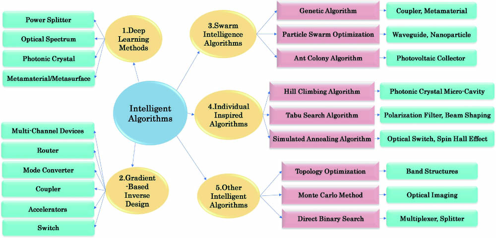
    Fig. 1. Summary of intelligent algorithms and their applications for designing nanophotonic devices in this review.
    Inclusion relation of machine learning, representation learning, deep learning, and artificial intelligence.
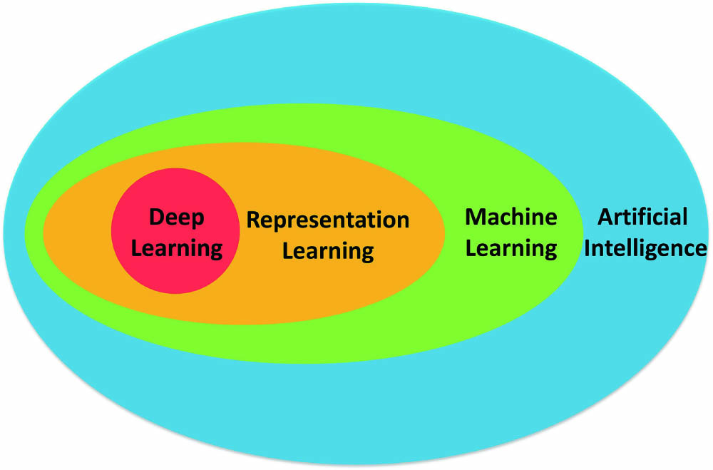
    Fig. 2. Inclusion relation of machine learning, representation learning, deep learning, and artificial intelligence.
    Neurons in each layer process and transfer data in the form of column vectors, and the weights of neural networks are expressed as matrices. The θ represents the element of the matrix Θ. It is worth noting that we did not list all the weights of layer I−1, but only the information processing of the first neuron in the Ith layer is shown here.
    Fig. 3. Neurons in each layer process and transfer data in the form of column vectors, and the weights of neural networks are expressed as matrices. The θ represents the element of the matrix Θ. It is worth noting that we did not list all the weights of layer I1, but only the information processing of the first neuron in the Ith layer is shown here.
    (a) Bidirectional network used for inverse design[13]. (b) The TN consists of an inverse design network and a forward modeling network[14]. (c) A CNN consists of two bidirectional neural networks, and it is capable of automatically designing and optimizing three-dimensional (3D) chiral metamaterials with strong chiral-optical responses at specified wavelengths[17]. (d) A DNN for forward and inverse design of a power splitter[16].
    Fig. 4. (a) Bidirectional network used for inverse design[13]. (b) The TN consists of an inverse design network and a forward modeling network[14]. (c) A CNN consists of two bidirectional neural networks, and it is capable of automatically designing and optimizing three-dimensional (3D) chiral metamaterials with strong chiral-optical responses at specified wavelengths[17]. (d) A DNN for forward and inverse design of a power splitter[16].
    (a) CNN used to predict the invariance of 1D photonic crystal[18]. (b) A novel CAVE for the design of a power splitter[23].
    Fig. 5. (a) CNN used to predict the invariance of 1D photonic crystal[18]. (b) A novel CAVE for the design of a power splitter[23].
    Nanophotonic devices designed by the gradient-based inverse design. (a) The structure diagram of 2×2×2 hub[62]. (b) The electromagnetic energy density of the hub about the fundamental TE-polarized mode at either 1550 nm or 1310 nm. (c) Performance specification of the TE mode converter[62]. (d) and (e) 1×3 power router with 500 nm wide input and output waveguides[60]: (d) SEM image of the fabricated router; (e) the electromagnetic energy density of the power router at 1550 nm.
    Fig. 6. Nanophotonic devices designed by the gradient-based inverse design. (a) The structure diagram of 2×2×2 hub[62]. (b) The electromagnetic energy density of the hub about the fundamental TE-polarized mode at either 1550 nm or 1310 nm. (c) Performance specification of the TE mode converter[62]. (d) and (e) 1×3 power router with 500 nm wide input and output waveguides[60]: (d) SEM image of the fabricated router; (e) the electromagnetic energy density of the power router at 1550 nm.
    Nanophotonic devices designed by the gradient-based inverse design. (a) The structure diagram of TE/TM router[62]. (b) The Electromagnetic energy density of the TE/TM router at 1550 nm. (c) Measured transmission of the three-channel router[65]. (d) Simulated electromagnetic energy density of the three-channel router at the three operating wavelengths.
    Fig. 7. Nanophotonic devices designed by the gradient-based inverse design. (a) The structure diagram of TE/TM router[62]. (b) The Electromagnetic energy density of the TE/TM router at 1550 nm. (c) Measured transmission of the three-channel router[65]. (d) Simulated electromagnetic energy density of the three-channel router at the three operating wavelengths.
    Nanophotonic devices designed by the gradient-based inverse design. (a) SEM image of cascaded Fano–Lorentzian resonators implemented on a silicon-on-insulator platform[67]. (b) The R=94% reflector used to implement a Lorentzian resonator. Top: optimization trajectory to obtain the desired non-resonant high reflection; bottom: low-power transmission of a single device with non-resonant reflection R=94% and red line is a fit with a Lorentzian line shape. (c) A conceptual photonic circuit that consists of a grating coupler followed by a waveguide-splitter and two resonators, and the outputs of them are then recombined in a waveguide-splitter and coupled off-chip through a grating coupler[61]. (d) Spectra of the nano-beams from the device shown in (a). The green, black, and red data correspond to the upper, both, and the lower nano-beam, respectively. (e) Demonstration that cavities with a fabrication-induced frequency offset can be tuned in resonance via gas tuning; the color bar corresponds to normalized counts.
    Fig. 8. Nanophotonic devices designed by the gradient-based inverse design. (a) SEM image of cascaded Fano–Lorentzian resonators implemented on a silicon-on-insulator platform[67]. (b) The R=94% reflector used to implement a Lorentzian resonator. Top: optimization trajectory to obtain the desired non-resonant high reflection; bottom: low-power transmission of a single device with non-resonant reflection R=94% and red line is a fit with a Lorentzian line shape. (c) A conceptual photonic circuit that consists of a grating coupler followed by a waveguide-splitter and two resonators, and the outputs of them are then recombined in a waveguide-splitter and coupled off-chip through a grating coupler[61]. (d) Spectra of the nano-beams from the device shown in (a). The green, black, and red data correspond to the upper, both, and the lower nano-beam, respectively. (e) Demonstration that cavities with a fabrication-induced frequency offset can be tuned in resonance via gas tuning; the color bar corresponds to normalized counts.
    The flow chart of GA[77].
    Fig. 9. The flow chart of GA[77].
    Nanophotonic devices designed by GA. (a) Lattice optical materials capable of focusing light into several different focal points in the far field. The left is a schematic diagram of the experimental device. The right shows light focused on several different points through a lattice of lattice optical materials[6]. (b) Simulated reflection characteristics of antireflection coatings[76]. (c) The left is the initial silicon plate and the corresponding electric field distribution before optimization, and the right is the structure and electric field distribution of the reflector after optimization[77]. (d) The structure obtained after GA and simulated transmittance spectrum[78].
    Fig. 10. Nanophotonic devices designed by GA. (a) Lattice optical materials capable of focusing light into several different focal points in the far field. The left is a schematic diagram of the experimental device. The right shows light focused on several different points through a lattice of lattice optical materials[6]. (b) Simulated reflection characteristics of antireflection coatings[76]. (c) The left is the initial silicon plate and the corresponding electric field distribution before optimization, and the right is the structure and electric field distribution of the reflector after optimization[77]. (d) The structure obtained after GA and simulated transmittance spectrum[78].
    Nanophotonic devices designed by GA. (a) The structure diagram of wavelength router and (b) the simulated transmittance[7]. (c) The optimized structure of the polarization router. (d) and (e) are the simulated transmission spectra of the polarization router’s O1 and O2 ports[8].
    Fig. 11. Nanophotonic devices designed by GA. (a) The structure diagram of wavelength router and (b) the simulated transmittance[7]. (c) The optimized structure of the polarization router. (d) and (e) are the simulated transmission spectra of the polarization router’s O1 and O2 ports[8].
    Nanophotonic devices designed by GA. (a) Measured data and calculated results (red solid line), the illustration is a schematic of carbon nanotube films and diode FE measurements. (b) Optimized electron beam trajectories for type of FE device[79]. (c) The total scattering efficiency of normalization (black line), and the contribution of induced electric dipole (ED) and magnetic dipole (MD) moments of core-shell nanoparticles[80].
    Fig. 12. Nanophotonic devices designed by GA. (a) Measured data and calculated results (red solid line), the illustration is a schematic of carbon nanotube films and diode FE measurements. (b) Optimized electron beam trajectories for type of FE device[79]. (c) The total scattering efficiency of normalization (black line), and the contribution of induced electric dipole (ED) and magnetic dipole (MD) moments of core-shell nanoparticles[80].
    Nanophotonic devices designed by PSO. (a) A notch filter based on microcavity and (b) single frame extract video recording of the electric field intensity of the notch filter at the wavelength of 1500 nm[86]. (c) The structure of the tapered PSO and the distribution inside the electric field[5]. (d) The optimized geometry of the silver nanoparticles array and (e) the magnitude of its Fourier transform[87].
    Fig. 13. Nanophotonic devices designed by PSO. (a) A notch filter based on microcavity and (b) single frame extract video recording of the electric field intensity of the notch filter at the wavelength of 1500 nm[86]. (c) The structure of the tapered PSO and the distribution inside the electric field[5]. (d) The optimized geometry of the silver nanoparticles array and (e) the magnitude of its Fourier transform[87].
    Nanophotonic devices designed by PSO. (a) The SEM image of SOL and (b) the SEM image of the cluster of nanoholes on the metal membrane. The SOL image shows all the main features of the cluster[88]. (c) Optimized power splitter device and (d) normalized strength[90]. (e) The white rectangle represents the spatial distribution of the nanometer aperture of the two-channel multiplexing lens. (f) The simulated intensity profiles of the radiated beam of the two-channel multiplexing metalens in the xz plane[91].
    Fig. 14. Nanophotonic devices designed by PSO. (a) The SEM image of SOL and (b) the SEM image of the cluster of nanoholes on the metal membrane. The SOL image shows all the main features of the cluster[88]. (c) Optimized power splitter device and (d) normalized strength[90]. (e) The white rectangle represents the spatial distribution of the nanometer aperture of the two-channel multiplexing lens. (f) The simulated intensity profiles of the radiated beam of the two-channel multiplexing metalens in the xz plane[91].
    The flow chart of ACA optimization process[94].
    Fig. 15. The flow chart of ACA optimization process[94].
    Nanophotonic devices designed by ACA. (a) The ACA-based method was used to calculate the reflection coefficient of the antireflection coating system on silicon substrate and (b) the simulation results show that the reflectivity of the antireflection coating system is changed with wavelength and incident angle by ACA[95].
    Fig. 16. Nanophotonic devices designed by ACA. (a) The ACA-based method was used to calculate the reflection coefficient of the antireflection coating system on silicon substrate and (b) the simulation results show that the reflectivity of the antireflection coating system is changed with wavelength and incident angle by ACA[95].
    The flow chart of SAA[98].
    Fig. 17. The flow chart of SAA[98].
    Nanophotonic devices designed by SAA. (a) A schematic of the twisted light emitter. (b) Details of structure parameters. R (R=1200 nm) stands for the radius of the device, H (H=220 nm) the height and W (W=440 nm) the width of the waveguide. The red arrow represents light from the left waveguide. Φ1 and Φ2 represents the propagating phase modulation and resonance modulation, respectively. Here, a scanning electron microscope image of the fabricated OAM is presented[102]. (c) FDTD simulation result and experiment data of the OAM emitter.
    Fig. 18. Nanophotonic devices designed by SAA. (a) A schematic of the twisted light emitter. (b) Details of structure parameters. R (R=1200nm) stands for the radius of the device, H (H=220nm) the height and W (W=440nm) the width of the waveguide. The red arrow represents light from the left waveguide. Φ1 and Φ2 represents the propagating phase modulation and resonance modulation, respectively. Here, a scanning electron microscope image of the fabricated OAM is presented[102]. (c) FDTD simulation result and experiment data of the OAM emitter.
    Nanophotonic devices designed by SAA. (a) Schematic of the photonic spin element. Incident light is coupled into different waveguides according to the spin states. (b) The core component of an optical element. The design area is divided into 288 pixels. The green blocks stand for optimized structures filled with silicon and the white blocks stand for air. (c) The measured output power at different ports when the polarization of incident light varies[103].
    Fig. 19. Nanophotonic devices designed by SAA. (a) Schematic of the photonic spin element. Incident light is coupled into different waveguides according to the spin states. (b) The core component of an optical element. The design area is divided into 288 pixels. The green blocks stand for optimized structures filled with silicon and the white blocks stand for air. (c) The measured output power at different ports when the polarization of incident light varies[103].
    Nanophotonic devices designed by the hill-climbing algorithm. (a) An example of the target function in which the difficulties of hill climbing are shown. (b) The schematic of the photonic crystal split-beam nanocavity. R1, R2, and R3 are optimized by the algorithm. Experimental transmission spectrum of the split-beam cavity under 0.6 mW input power respectively in the whole measurement range, (c) the 2nd TE mode individually and (d) the 4th TE mode individually[105].
    Fig. 20. Nanophotonic devices designed by the hill-climbing algorithm. (a) An example of the target function in which the difficulties of hill climbing are shown. (b) The schematic of the photonic crystal split-beam nanocavity. R1, R2, and R3 are optimized by the algorithm. Experimental transmission spectrum of the split-beam cavity under 0.6 mW input power respectively in the whole measurement range, (c) the 2nd TE mode individually and (d) the 4th TE mode individually[105].
    (a) Flowchart of the hill climbing algorithm. (b) An example of the target function in which the difficulties of hill climbing are shown.
    Fig. 21. (a) Flowchart of the hill climbing algorithm. (b) An example of the target function in which the difficulties of hill climbing are shown.
    The flowchart of TS.
    Fig. 22. The flowchart of TS.
    Nanophotonic devices designed by TS. (a) Basic photonic lattice configuration for the beam shaping problem. (b) Best possible trade-off between the amplitude and the phase profile of the beam in the beam shaping problem[109]. (c) The |Ez| field profile (arbitrary units) and comparison of orthogonal polarization components along target plane of optimized TM polarized Gaussian beam. (d) The |Hz| field profile (arbitrary units) and comparison of orthogonal polarization components along target plane of optimized TE polarized Gaussian beam[110].
    Fig. 23. Nanophotonic devices designed by TS. (a) Basic photonic lattice configuration for the beam shaping problem. (b) Best possible trade-off between the amplitude and the phase profile of the beam in the beam shaping problem[109]. (c) The |Ez| field profile (arbitrary units) and comparison of orthogonal polarization components along target plane of optimized TM polarized Gaussian beam. (d) The |Hz| field profile (arbitrary units) and comparison of orthogonal polarization components along target plane of optimized TE polarized Gaussian beam[110].
    The flow chart of DBS algorithm[112].
    Fig. 24. The flow chart of DBS algorithm[112].
    Nanophotonic devices designed by DBS. (a) Panel a, structure diagram of a free-space to multi-mode waveguide coupler and polarization splitter; panels b and c are simulated time-averaged intensity distribution for light polarized along X and that polarized along Y, respectively[120]. (b) The structure diagram of a polarization splitter. (c) and (d) The simulated steady-state intensity distributions for TE and TM polarized light at the design wavelength of 1550 nm, respectively[113]. (e) and (f) Reference coupled system and the cloak for micro-ring resonator[124].
    Fig. 25. Nanophotonic devices designed by DBS. (a) Panel a, structure diagram of a free-space to multi-mode waveguide coupler and polarization splitter; panels b and c are simulated time-averaged intensity distribution for light polarized along X and that polarized along Y, respectively[120]. (b) The structure diagram of a polarization splitter. (c) and (d) The simulated steady-state intensity distributions for TE and TM polarized light at the design wavelength of 1550 nm, respectively[113]. (e) and (f) Reference coupled system and the cloak for micro-ring resonator[124].
    Nanophotonic devices designed by DBS. (a) The top-view microscope image of the mode-division multiplexing circuit (top), and the lower left corner is the microscope image of the four-cascaded crossing[126]. (b) The scanning electron microscope image. (c) The measured transmission spectra for the mode-division multiplexing circuit. (d) The top view of the 1 × 4 power splitter (top), and the bottom is optical field distribution[129]. (e) Excess loss of each output port.
    Fig. 26. Nanophotonic devices designed by DBS. (a) The top-view microscope image of the mode-division multiplexing circuit (top), and the lower left corner is the microscope image of the four-cascaded crossing[126]. (b) The scanning electron microscope image. (c) The measured transmission spectra for the mode-division multiplexing circuit. (d) The top view of the 1 × 4 power splitter (top), and the bottom is optical field distribution[129]. (e) Excess loss of each output port.
    (a) The structure of the topology optimization algorithm used in the work. (b) The 3D model of gold nanoparticle dimer with predefined key parameters in geometry and material.
    Fig. 27. (a) The structure of the topology optimization algorithm used in the work. (b) The 3D model of gold nanoparticle dimer with predefined key parameters in geometry and material.
    Nanophotonic devices designed by the level set method. (a) The evolution of the dielectric distribution[133]. (b) The bandgap versus the iteration. (c) The final band structure with the largest bandgap between ωTM1 and ωTM2.
    Fig. 28. Nanophotonic devices designed by the level set method. (a) The evolution of the dielectric distribution[133]. (b) The bandgap versus the iteration. (c) The final band structure with the largest bandgap between ωTM1 and ωTM2.
    Intelligent Design AlgorithmsAdvantagesDisadvantagesUnique FeaturesSuitable Design for Photonic Structures and Devices
    1. Deep learning methodsSpend less time than traditional algorithms (after training). More likely to find better local optimal solutions. Many typical structures and strong flexibility. Realize inverse design more easily.Take a lot of computational and time cost for preparation and training. Difficult to exploit the trained ANN for further analysis. Poor performance when dealing with problems with few samples.Great for dealing with problems that training set is easy to generate. Ability of transfer learning (albeit immature). Some hyperparameters need to be tweaked.Nanoparticle[51], power splitter[16,23], optical spectrum[34,37,50,52], metamaterial[17], metasuface[21,49]
    2. Gradient-based inverse design algorithmLarge parameter space, high computational efficiency.Exhibit a continuous topography, produce a local optimal solution.Gradient-based, large parameter space.Multi-channel devices[62], router[6062,64,65,67], coupler[63], mode converter[62], accelerators[66], switch[68]
    3. Genetic algorithmSuitable for solving complex optimization problems, concurrency, extensibility.Low search efficiency in late evolution, premature convergence.Large coverage, self-organization, self-adaptation, self-learning.Coupler[78], metamaterial[6], nanoparticle[80], router[79]
    4. Particle swarm optimizationFast convergence speed, easily understood, parallel computing.High requirement for parameter setting.Real-time change of perception.Waveguide[5], nanoparticle[87]
    5. Ant colony algorithmSuitable for combinatorial and continuous function optimization, intuitive.High time cost.Usually combined with other algorithms.Photovoltaic collector[95]
    6. Simulated annealing algorithmRobustness of a random initial guess, simple structure, parallel computing.Sensitive to parameters, low efficiency.Converge with the drop of temperature.Coupler[103], switch[99], metamaterial[139]
    7. Hill-climbing algorithmEasily understood, avoid traversal in solution space.Unable to break out the local optimum.One of the most basic heuristic algorithms.Nano-cavity[104]
    8. Tabu search algorithmSuitable for combinatorial optimization, fast convergence speed.Premature convergence, high requirement for parameter setting.Parallel tabu search can improve efficiency.Polarization filter[110], beam shaping device[109]
    9. Direct binary searchDiscrete structure generated by DBS algorithms is more favorable to the fabrication.Suitable for small parameter space, computationally expensive, sensitive to the starting point.A simpler iterative algorithm.Coupler[120], computational microscopy[121], polarizer[115], router[113,122,128,129], optical modulator[123], integrated cloak[124]
    10. Topology optimizationLarge degree of freedom in design, high sustainability.Complex shapes are difficult to manufacture.Optimize the material distribution.Band structures[133]
    11. Monte Carlo methodStrong adaptability.Assumptions need to be fair.Solve problems without analytical solutions.Optical imaging[140]
    Table 1. Comparison of Various Intelligent Design Algorithms
    Lifeng Ma, Jing Li, Zhouhui Liu, Yuxuan Zhang, Nianen Zhang, Shuqiao Zheng, Cuicui Lu. Intelligent algorithms: new avenues for designing nanophotonic devices [Invited][J]. Chinese Optics Letters, 2021, 19(1): 011301
    Download Citation