
Tongtong Kang, Boyu Fan, Jun Qin, Weihao Yang, Shuang Xia, Zheng Peng, Bo Liu, Sui Peng, Xiao Liang, Tingting Tang, Longjiang Deng, Yi Luo, Hanbin Wang, Qiang Zhou, Lei Bi. Mid-infrared active metasurface based on Si/VO2 hybrid meta-atoms[J]. Photonics Research, 2022, 10(2): 373
- Photonics Research
- Vol. 10, Issue 2, 373 (2022)
Abstract
1. INTRODUCTION
All-dielectric metasurfaces enabling light manipulation in two-dimensional photonic nanostructures have attracted great research interest recently. Compared to plasmonic devices, all-dielectric metasurfaces show characteristics of low optical absorption and unique Mie resonant modes [1–6]. A variety of novel photonic devices based on all-dielectric metasurfaces have been developed, including metalens [7–10], beam steerers [11–13], polarizers [14], and optical holography [15–21]. In the mid-infrared wavelength range, all-dielectric metasurfaces are promising for sensing, multispectral imaging, emissivity control, and infrared camouflage applications [22–27]. Nevertheless, most all-dielectric metasurfaces in the mid-infrared are static with fixed optical properties by design, which limit their application for tunable photonic devices.
Recently, active metasurfaces based on phase-change materials have attracted great research interest [28–37]. Phase-change materials such as (GST) and show large refractive index change () in the visible to far-infrared wavelength range upon phase transition (PT). For GST, the large refractive index contrast is attributed to the nonvolatile process, which has been widely utilized for reconfigurable metasurfaces, including tunable color display [38], varifocal metalenses [7,39], beam-steering devices [40], switches [41], and tunable thermal absorbers [42], etc. Compared to GST, the PT process of is volatile, which also shows much lower PT temperature than GST (68°C versus 600°C). Therefore, is better fitted for the photonic devices requiring dynamic and continuous modulation. For instance, has been applied for adaptive thermal camouflage [43], optical modulators [34,44], and tunable absorbers/emitters [45,46]. Recently, -based active all-dielectric metasurfaces have been developed. is either used as the only material to form Mie resonators, or incorporated in Mie resonators as the substrate or superstrate. Tunable Mie resonances based on nanodisks in the visible wavelength range were reported [47]. Optical limiting effect based on Huygens’ metasurfaces using nanodisks was experimentally observed [4]. Amplitude or spectral tuning was demonstrated in -based all-dielectric metasurfaces [48]. Apart from the phase change materials, other active materials are also employed to the reconfigurable metasurface devices, such as liquid crystal [49], graphene [50,51], InSb [52], and magnesium [53]. These devices show excellent tunability of the transmission spectrum in the visible to near-infrared, highlighting a promising potential for future device applications.
Here, we report a -based active all-dielectric metasurface in the mid-infrared wavelength range. Compared to previous reports, we made a step further by experimentally incorporating thin films in different locations of a silicon nanodisk Mie resonator and demonstrated its tunable transmittance spectrum in the mid-infrared. We show experimentally and theoretically that the insulator to metal phase transition (IMT) of influences the scattering cross section of Mie resonance modes differently, which strongly depends on the film locations. By judiciously designing and fabricating at the bottom or the middle of the Si Mie resonators, we show selective modulation of the scattering cross section of magnetic dipole or electric dipole resonances, respectively. We experimentally demonstrated a large modulation of the transmittance from 82% to 28% at 4.6 μm wavelength. These results indicate a promising potential of -based active metasurface for mid-infrared photonic device applications, such as infrared camouflage, chemical/biomedical sensing, optical neuromorphic computing, and multispectral imaging.
Sign up for Photonics Research TOC. Get the latest issue of Photonics Research delivered right to you!Sign up now
2. EXPERIMENTAL PROCEDURE
Figure 1(a) shows the schematic of the -based metasurfaces. The device consists of an array of hybrid nanodisks fabricated on a double side polished substrate. Two devices with at different locations of the meta-atoms were fabricated, namely hybrid metasurface with at the bottom of /HMB, and hybrid metasurface with in the middle of , respectively. The hybrid Mie resonators were fabricated by e-beam lithography (EBL) and deep reactive ion etching (DRIE) after deposition of and films on , as shown Fig. 1(a) (see details in Appendix A). Figures 1(b) and 1(c) show the scanning electron microscope (SEM) images of the two fabricated devices. The period of the nanodisks is 2.5 μm for both devices. The thickness of for both cases is 100 nm. The disk radius for both metasurfaces is 0.62 μm. The height for the HMB device is 0.9 μm, whereas the up and bottom silicon film thicknesses and for the HMM device are 570 nm and 330 nm, respectively.
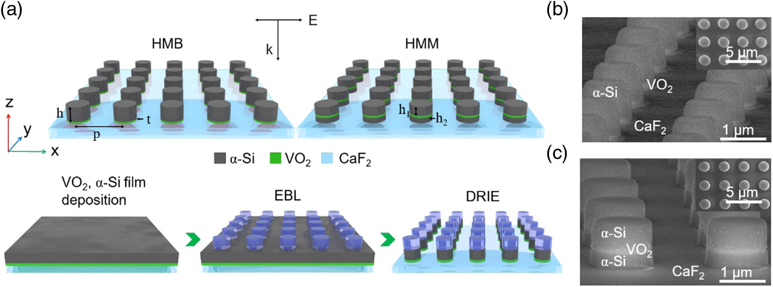
Figure 1.Device structure and process flow. (a) Process flow and schematics of the two hybrid α-
3. RESULTS AND DISCUSSION
Figures 2(a) and 2(c) show the simulated transmittance spectra of the HMB and HMM. Considering the trapezoid shape of the fabricated nanodisks shown in Figs. 1(b) and 1(c), the structures of our simulation are optimized to well match with the experiment results. The spectrum shows two dips at 3.6 μm and 4.2 μm, corresponding to the electric dipole resonance (ED) and magnetic dipole resonance (MD) modes, respectively. We observe the disappearance of the MD mode at the wavelength of 4.2 μm when changes from the dielectric to the metallic state, as shown in Fig. 2(a). For the ED mode, only a slight blueshift of the resonance peak and linewidth broadening are observed upon dielectric to metal phase transition. Figure 2(b) shows the transmittance spectra of the HMB device measured using a Fourier transform infrared (FTIR) spectrometer (see Appendix B), which matches with the simulation very well. For dielectric state , the ED and MD modes are observed at 3.7 μm and 4.2 μm wavelengths, respectively. After phase transition of to the metallic state, the MD mode disappears and the ED mode shifts to a shorter wavelength of 3.6 μm with a broader linewidth, which are consistent with the simulation results. The results are quite different for the HMM device. Figure 2(c) shows the simulated transmittance spectra for the HMM device. The ED mode disappears when changes from the dielectric to the metallic state, whereas the MD mode remains. The resonance wavelength of the MD mode redshifts from 4.2 μm to 4.5 μm with a slight linewidth broadening. Figure 2(d) shows the measured transmittance spectra for the HMM device, which also match with the simulation results. Upon insulator to metal phase transition, the ED mode disappears, whereas the MD mode redshifts from 4.2 μm to 4.5 μm. Here, the shift of the MD upon phase transition in our experiment is comparable to the simulation results, demonstrating that was not influenced by the etching process. Wavelength shift of the MD mode leads to a large intensity modulation amplitude from 82% to 28% at 4.6 μm wavelength. Interestingly, if we compare the transmittance spectra at the dielectric state for HMB and HMM samples, both in simulation and experiment, we notice they are almost the same. This is because and -Si show similar index of refraction at the mid-infrared wavelength range. Therefore, the transmittance spectrum shows little dependence on the thin film location. However, after insulator to metal phase transition, the two samples show drastically different transmittance spectra. This result highlights that engineering the film location in the meta-atom can significantly influence the optical property of the active metasurfaces. The simulated transmission phases of both metasurfaces are shown in Figs. 2(e) and 2(f). MD and ED resonances disappear for the HMB and HMM devices, respectively, resulting in clear phase modulation around the resonance wavelengths.
![]()
Figure 2.Tunable optical properties of HMB and HMM configurations. (a) Simulated and (b) measured transmittance spectra of the HMB configuration at dielectric and metallic states. (c) Simulated and (d) measured transmittance spectra of HMM configuration at dielectric and metallic states. Simulated transmission phase spectra of (e) HMB and (f) HMM configurations at dielectric and metallic states.
In order to study the mechanism of the active metasurface, near-field modal distributions of both the HMB and HMM devices are simulated, as shown in Fig. 3. Figure 3(a) shows the normalized electric field profiles of the ED mode at around 3.6 μm wavelength in the x–z plane of the HMB device. The color contour indicates the electric field profile. The white arrows indicate the electric field vector distribution. When is at the dielectric state (left), the electric field is centered in the nanodisk and mostly points along the x direction. Only a small amount of the electric field is distributed in the layer. Therefore, after IMT, the electric field becomes only slightly weaker in the Si nanoresonator, as shown by the right panel of Fig. 3(a). The higher absorption loss of the metallic also causes a broader linewidth of the ED mode, as shown in Figs. 2(a) and 2(b). The case is different for the MD mode, as shown in Fig. 3(b). The electric field forms current loops which are largely confined in the layer for the dielectric state. After IMT, the electric field is mostly absorbed by the metallic , as shown in the right panel of Fig. 3(b). The electric current loops disappear, causing the disappearance of the MD resonance mode. Similarly, we simulated the modal profiles of the HMM device, as shown in Figs. 3(c) and 3(d). When is at the dielectric state [the left panels of Figs. 3(c) and 3(d)], the electric field distribution is similar to the HMB devices. This explains the similarity of the measured transmittance spectra between Figs. 2(b) and 2(d). However, when the changes to the metallic state, the modal profile is very different for the HMM device. As shown by the right panel of Fig. 3(c), the electric field is strongly attenuated because is located at the antinode of the electric field, causing the disappearance of the ED mode. For the MD mode shown in the right panel of Fig. 3(d), the electric field is only partly absorbed by the very thin metallic film. The electric current loop and the MD mode still remain. The MD mode is redshifted due to a higher refractive index of the metallic . Similarly, due to the absorption loss of the metallic , a broader linewidth is observed for the MD mode, as shown in Figs. 2(c) and 2(d).
![]()
Figure 3.Modal profiles of the HMB and HMM devices at ED and MD wavelengths, for both the dielectric state (D state) and the metallic state (M state). (a) Electric field distributions of ED mode at the dielectric state (left) and the metallic state (right) for the HMB device. (b) Electric field distributions of MD mode at the dielectric state (left) and the metallic state (right) for the HMB device. (c) Electric field distributions of the ED mode for the dielectric state (left) and the metallic state (right) of the HMM device. (d) Electric field distributions of MD mode for the dielectric state (left) and the metallic state (right) of the HMM device.
![]()
Figure 4.Multipolar decomposition of the scattering cross sections. Scattering cross-section spectra of ED and MD modes of (a) HMB and (b) HMM configurations at the dielectric and metallic states. Simulated and fitted transmission spectra of (c) HMB and (d) HMM configurations for different metallic fractions of
4. CONCLUSION
In summary, we demonstrate a mid-infrared active metasurface based on hybrid nanoresonators. By incorporating at the bottom or middle of α-Si nanoresonators, we show similar transmittance spectra of the two metasurfaces for the dielectric state, but drastically different transmittance spectra for the metallic state. Based on modal analysis, multipolar decomposition and TCMT fitting, we show that varying the location of thin films induces different absorption loss of the Mie resonance modes, leading to almost independent tuning of the Mie resonance scattering cross sections for the ED and MD modes. The -based active all-dielectric metasurface is promising for mid-infrared photonic applications such as infrared camouflage, chemical/biomedical sensing, optical neuromorphic computing, and multispectral imaging.
Acknowledgment
Acknowledgment. L. B. and T. K. conceived and designed the experiment. T. K. and B. F. performed the sample fabrication, and L. B. and J. Q. supervised the project. All authors discussed the research.
APPENDIX A: SAMPLE FABRICATION
The multilayer thin films were deposited on double polished substrates by magnetron sputtering (Leybold, UNIVEX400CF), pulsed laser deposition (TSST), and plasma-enhanced chemical vapor deposition (PECVD, Trion). To promote adhesion, a 10 nm thick film was first deposited on the substrate by magnetron sputtering under 3.7 mTorr Ar ambient at room temperature. A 100 nm thick thin film was then deposited on the film by pulsed laser deposition at room temperature using a 248 nm KrF excimer laser. The laser fluence was . The deposition oxygen partial pressure was 14 mTorr. After deposition, the film was crystallized by
The hybrid meta-atoms were fabricated by EBL and inductively coupled plasma-reactive ion etching (ICP-RIE). First, a 120 nm thick hydrogen silsesquioxane resist layer was spin-coated on the multilayer films with a spin speed of 4000 r/min. The sample was then baked on a hot plate for 1 min at 150°C. Then the nanodisk patterns were exposed by EBL using an acceleration voltage of 10 kV and an average dose of . After exposure, the sample was developed in a mixed solution of (1/4/100) for 3 min and rinsed in de-ionized water for 1 min. After that, the top Si film was first etched in plasma in an ICP-RIE system under 7.5 mTorr pressure. The powers of ICP and RIE were 500 W and 40 W, respectively. Finally, the film was etched in a , , and plasma mixture under 35 mTorr pressure with an RIE power of 20 W.
APPENDIX B: OPTICAL CHARACTERIZATION
The transmission spectra were measured by an FTIR spectrometer (Perkin Elmer) equipped with a reflective focusing infrared microscope (Spotlight 2000i). The spot size was . To induce the phase transition of , a hot plate was used to heat the sample in the 20°C–100°C temperature range.
APPENDIX C: SIMULATION AND MULTIPOLAR DECOMPOSITION
The simulation of the transmittance spectra and near-field modal profiles was performed using the commercial software COMSOL Multiphysics. Periodic boundary conditions were used around the nanodisks. The port boundary condition was used to define the polarization and angle of incidence. To avoid the effect of scattered light, a perfectly matched layer was set at the top and bottom layers near the port. The transmittance spectra were calculated using the simulated S parameters in COMSOL. The optical constants of were adopted from Ref. [
To perform multipolar decomposition, we calculated the scattering field of the nanodisks embedded in a homogeneous medium using COMSOL. periodic nanodisks were used in our simulation to resemble the scattering field of the periodic nanodisks. The total electric fields were extracted from COMSOL, and the displacement current was defined as
References
[1] J. Tian, H. Luo, Y. Yang, F. Ding, Y. Qu, D. Zhao, M. Qiu, S. I. Bozhevolnyi. Active control of anapole states by structuring the phase-change alloy Ge2Sb2Te5. Nat. Commun., 10, 396(2019).
[2] D. R. Abujetas, Á. Barreda, F. Moreno, A. Litman, J. M. Geffrin, J. A. Sánchez-Gil. High-
[3] H. M. Doeleman, F. Monticone, W. Den Hollander, A. Alù, A. F. Koenderink. Experimental observation of a polarization vortex at an optical bound state in the continuum. Nat. Photonics, 12, 397-401(2018).
[4] A. Howes, Z. Zhu, D. Curie, J. R. Avila, V. D. Wheeler, R. F. Haglund, J. G. Valentine. Optical limiting based on Huygens’ metasurfaces. Nano Lett., 20, 4638-4644(2020).
[5] A. Howes, W. Wang, I. Kravchenko, J. Valentine. Dynamic transmission control based on all-dielectric Huygens metasurfaces. Optica, 5, 787-792(2018).
[6] S. Yuan, X. Qiu, C. Cui, L. Zhu, Y. Wang, Y. Li, J. Song, Q. Huang, J. Xia. Strong photoluminescence enhancement in all-dielectric Fano metasurface with high quality factor. ACS Nano, 11, 10704-10711(2017).
[7] M. Y. Shalaginov, S. An, Y. Zhang, F. Yang, P. Su, V. Liberman, J. B. Chou, C. M. Roberts, M. Kang, C. Rios, Q. Du, C. Fowler, A. Agarwal, K. A. Richardson, C. Rivero-Baleine, H. Zhang, J. Hu, T. Gu. Reconfigurable all-dielectric metalens with diffraction-limited performance. Nat. Commun., 12, 1225(2021).
[8] S. Gao, C. S. Park, C. Zhou, S. S. Lee, D. Y. Choi. Twofold polarization-selective all-dielectric trifoci metalens for linearly polarized visible light. Adv. Opt. Mater., 7, 1900883(2019).
[9] C. Schlickriede, S. S. Kruk, S. S. Kruk, L. Wang, B. Sain, Y. Kivshar, T. Zentgraf. Nonlinear imaging with all-dielectric metasurfaces. Nano Lett., 20, 4370-4376(2020).
[10] L. Yu, Y. Fan, Y. Wang, C. Zhang, W. Yang, Q. Song, S. Xiao. Spin angular momentum controlled multifunctional all-dielectric metasurface doublet. Laser Photonics Rev., 14, 1900324(2020).
[11] S. Q. Li, X. Xu, R. M. Veetil, V. Valuckas, R. Paniagua-Domínguez, A. I. Kuznetsov. Phase-only transmissive spatial light modulator based on tunable dielectric metasurface. Science, 364, 1087-1090(2019).
[12] T. Shi, Y. Wang, Z. L. Deng, X. Ye, Z. Dai, Y. Cao, B. O. Guan, S. Xiao, X. Li. All-dielectric kissing-dimer metagratings for asymmetric high diffraction. Adv. Opt. Mater., 7, 1901389(2019).
[13] P. C. Wu, R. A. Pala, G. Kafaie Shirmanesh, W. H. Cheng, R. Sokhoyan, M. Grajower, M. Z. Alam, D. Lee, H. A. Atwater. Dynamic beam steering with all-dielectric electro-optic III–V multiple-quantum-well metasurfaces. Nat. Commun., 10, 3654(2019).
[14] S. Wang, Z. L. Deng, Y. Wang, Q. Zhou, X. Wang, Y. Cao, B. O. Guan, S. Xiao, X. Li. Arbitrary polarization conversion dichroism metasurfaces for all-in-one full Poincaré sphere polarizers. Light Sci. Appl., 10, 24(2021).
[15] G. Qu, W. Yang, Q. Song, Y. Liu, C. W. Qiu, J. Han, D. P. Tsai, S. Xiao. Reprogrammable meta-hologram for optical encryption. Nat. Commun., 11, 5484(2020).
[16] S. Sun, W. Yang, C. Zhang, J. Jing, Y. Gao, X. Yu, Q. Song, S. Xiao. Real-time tunable colors from microfluidic reconfigurable all-dielectric metasurfaces. ACS Nano, 12, 2151-2159(2018).
[17] X. Zhang, Q. Wang, Q. Xu, X. Zhang, C. Tian, Y. Xu, J. Gu, Z. Tian, C. Ouyang, J. Han, W. Zhang. All-dielectric meta-holograms with holographic images transforming longitudinally. ACS Photonics, 5, 599-606(2018).
[18] M. A. Ansari, I. Kim, D. Lee, M. H. Waseem, M. Zubair, N. Mahmood, T. Badloe, S. Yerci, T. Tauqeer, M. Q. Mehmood, J. Rho. A spin-encoded all-dielectric metahologram for visible light. Laser Photonics Rev., 13, 1900065(2019).
[19] B. Reineke, B. Sain, R. Zhao, L. Carletti, B. Liu, L. Huang, C. De Angelis, T. Zentgraf. Silicon metasurfaces for third harmonic geometric phase manipulation and multiplexed holography. Nano Lett., 19, 6585-6591(2019).
[20] X. Guo, P. Li, J. Zhong, S. Liu, B. Wei, W. Zhu, S. Qi, H. Cheng, J. Zhao. Tying polarization-switchable optical vortex knots and links via holographic all-dielectric metasurfaces. Laser Photonics Rev., 14, 1900366(2020).
[21] Q. Wei, B. Sain, Y. Wang, B. Reineke, X. Li, L. Huang, T. Zentgraf. Simultaneous spectral and spatial modulation for color printing and holography using all-dielectric metasurfaces. Nano Lett., 19, 8964-8971(2019).
[22] K. Tang, X. Wang, K. Dong, Y. Li, J. Li, B. Sun, X. Zhang, C. Dames, C. Qiu, J. Yao, J. Wu. A thermal radiation modulation platform by emissivity engineering with graded metal–insulator transition. Adv. Mater., 32, 1907071(2020).
[23] L. Long, S. Taylor, L. Wang. Enhanced infrared emission by thermally switching the excitation of magnetic polariton with scalable microstructured VO2 metasurfaces. ACS Photonics, 7, 2219-2227(2020).
[24] K. Tang, K. Dong, C. J. Nicolai, Y. Li, J. Li, S. Lou, C. W. Qiu, D. H. Raulet, J. Yao, J. Wu. Millikelvin-resolved ambient thermography. Sci. Adv., 6, eabd8688(2020).
[25] H. Zuo, D. Y. Choi, X. Gai, P. Ma, L. Xu, D. N. Neshev, B. Zhang, B. Luther-Davies. High-efficiency all-dielectric metalenses for mid-infrared imaging. Adv. Opt. Mater., 5, 1700585(2017).
[26] C. Yan, X. Li, M. Pu, X. Ma, F. Zhang, P. Gao, K. Liu, X. Luo. Midinfrared real-time polarization imaging with all-dielectric metasurfaces. Appl. Phys. Lett., 114, 161904(2019).
[27] T. Lewi, N. A. Butakov, J. A. Schuller. Thermal tuning capabilities of semiconductor metasurface resonators. Nanophotonics, 8, 331-338(2018).
[28] S. An, C. Fowler, B. Zheng, M. Y. Shalaginov, H. Tang, H. Li, L. Zhou, J. Ding, A. M. Agarwal, C. Rivero-Baleine, K. A. Richardson, T. Gu, J. Hu, H. Zhang. A deep learning approach for objective-driven all-dielectric metasurface design. ACS Photonics, 6, 3196-3207(2019).
[29] C. H. Chu, M. L. Tseng, J. Chen, P. C. Wu, Y. H. Chen, H. C. Wang, T. Y. Chen, W. T. Hsieh, H. J. Wu, G. Sun, D. P. Tsai. Active dielectric metasurface based on phase-change medium. Laser Photonics Rev., 10, 986-994(2016).
[30] A. Leitis, A. Heßler, S. Wahl, M. Wuttig, T. Taubner, A. Tittl, H. Altug. All-dielectric programmable Huygens’ metasurfaces. Adv. Funct. Mater., 30, 1910259(2020).
[31] S. Abdollahramezani, O. Hemmatyar, M. Taghinejad, H. Taghinejad, Y. Kiarashinejad, M. Zandehshahvar, T. Fan, S. Deshmukh, A. A. Eftekhar, W. Cai, E. Pop, M. A. El-Sayed, A. Adibi. Dynamic hybrid metasurfaces. Nano Lett., 21, 1238-1245(2021).
[32] Y. Wang, P. Landreman, D. Schoen, K. Okabe, A. Marshall, U. Celano, H. S. P. Wong, J. Park, M. L. Brongersma. Electrical tuning of phase-change antennas and metasurfaces. Nat. Nanotechnol., 16, 667-672(2021).
[33] Y. Zhang, C. Fowler, J. Liang, B. Azhar, M. Y. Shalaginov, S. Deckoff-Jones, S. An, J. B. Chou, C. M. Roberts, V. Liberman, M. Kang, C. Ríos, K. A. Richardson, C. Rivero-Baleine, T. Gu, H. Zhang, J. Hu. Electrically reconfigurable non-volatile metasurface using low-loss optical phase-change material. Nat. Nanotechnol., 16, 661-666(2021).
[34] Y. Kim, P. C. Wu, R. Sokhoyan, K. Mauser, R. Glaudell, G. Kafaie Shirmanesh, H. A. Atwater. Phase modulation with electrically tunable vanadium dioxide phase-change metasurfaces. Nano Lett., 19, 3961-3968(2019).
[35] B. Gholipour, A. Karvounis, J. Yin, C. Soci, K. F. MacDonald, N. I. Zheludev. Phase-change-driven dielectric-plasmonic transitions in chalcogenide metasurfaces. NPG Asia Mater., 10, 533-539(2018).
[36] C. Ruiz De Galarreta, I. Sinev, A. M. Arseny, P. Trofimov, K. Ladutenko, S. G.-C. Carrillo, E. Gemo, A. Baldycheva, J. Bertolotti, C. D. Wright. Reconfigurable multilevel control of hybrid all-dielectric phase-change metasurfaces. Optica, 7, 476-484(2020).
[37] M. N. Julian, C. Williams, S. Borg, S. Bartram, H. J. Kim. Reversible optical tuning of GeSbTe phase-change metasurface spectral filters for mid-wave infrared imaging. Optica, 7, 746-754(2020).
[38] S. G. C. Carrillo, L. Trimby, Y. Y. Au, V. K. Nagareddy, G. Rodriguez-Hernandez, P. Hosseini, C. Ríos, H. Bhaskaran, C. D. Wright. A nonvolatile phase-change metamaterial color display. Adv. Opt. Mater., 7, 1801782(2019).
[39] X. Yin, T. Steinle, L. Huang, T. Taubner, M. Wuttig, T. Zentgraf, H. Giessen. Beam switching and bifocal zoom lensing using active plasmonic metasurfaces. Light Sci. Appl., 6, e17016(2017).
[40] C. R. de Galarreta, A. M. Alexeev, Y. Y. Au, M. Lopez-Garcia, M. Klemm, M. Cryan, J. Bertolotti, C. D. Wright. Nonvolatile reconfigurable phase-change metadevices for beam steering in the near infrared. Adv. Funct. Mater., 28, 1704993(2018).
[41] A. Ahmadivand, B. Gerislioglu, R. Sinha, M. Karabiyik, N. Pala. Optical switching using transition from dipolar to charge transfer plasmon modes in Ge2Sb2Te5 bridged metallodielectric dimers. Sci. Rep., 7, 42807(2017).
[42] A. Tittl, A. K. U. Michel, M. Schäferling, X. Yin, B. Gholipour, L. Cui, M. Wuttig, T. Taubner, F. Neubrech, H. Giessen. A switchable mid-infrared plasmonic perfect absorber with multispectral thermal imaging capability. Adv. Mater., 27, 4597-4603(2015).
[43] S. Chandra, D. Franklin, J. Cozart, A. Safaei, D. Chanda. Adaptive multispectral infrared camouflage. ACS Photonics, 5, 4513-4519(2018).
[44] P. Guo, M. S. Weimer, J. D. Emery, B. T. Diroll, X. Chen, A. S. Hock, R. P. H. Chang, A. B. F. Martinson, R. D. Schaller. Conformal coating of a phase change material on ordered plasmonic nanorod arrays for broadband all-optical switching. ACS Nano, 11, 693-701(2017).
[45] K. Sun, C. A. Riedel, A. Urbani, M. Simeoni, S. Mengali, M. Zalkovskij, B. Bilenberg, C. H. De Groot, O. L. Muskens. VO2 thermochromic metamaterial-based smart optical solar reflector. ACS Photonics, 5, 2280-2286(2018).
[46] J. Rensberg, S. Zhang, Y. Zhou, A. S. McLeod, C. Schwarz, M. Goldflam, M. Liu, J. Kerbusch, R. Nawrodt, S. Ramanathan, D. N. Basov, F. Capasso, C. Ronning, M. A. Kats. Active optical metasurfaces based on defect-engineered phase-transition materials. Nano Lett., 16, 1050-1055(2016).
[47] P. Kepič, F. Ligmajer, M. Hrtoň, H. Ren, L. D. S. Menezes, S. A. Maier, T. Šikola. Optically tunable Mie resonance VO2 nanoantennas for metasurfaces in the visible. ACS Photonics, 8, 1048-1057(2021).
[48] A. Tripathi, J. John, S. Kruk, Z. Zhang, H. S. Nguyen, L. Berguiga, P. R. Romeo, R. Orobtchouk, S. Ramanathan, Y. Kivshar, S. Cueff. Tunable Mie-resonant dielectric metasurfaces based on VO2 phase-transition materials. ACS Photonics, 8, 1206-1213(2021).
[49] Y. Hu, X. Ou, T. Zeng, J. Lai, J. Zhang, X. Li, X. Luo, L. Li, F. Fan, H. Duan. Electrically tunable multifunctional polarization-dependent metasurfaces integrated with liquid crystals in the visible region. Nano Lett., 21, 4554-4562(2021).
[50] B. Zeng, Z. Huang, A. Singh, Y. Yao, A. K. Azad, A. D. Mohite, A. J. Taylor, D. R. Smith, H. T. Chen. Hybrid graphene metasurfaces for high-speed mid-infrared light modulation and single-pixel imaging. Light Sci. Appl., 7, 51(2018).
[51] M. C. Sherrott, P. W. C. Hon, K. T. Fountaine, J. C. Garcia, S. M. Ponti, V. W. Brar, L. A. Sweatlock, H. A. Atwater. Experimental demonstration of >230° phase modulation in gate-tunable graphene-gold reconfigurable mid-infrared metasurfaces. Nano Lett., 17, 3027-3034(2017).
[52] P. P. Iyer, M. Pendharkar, C. J. Palmstrøm, J. A. Schuller. Ultrawide thermal free-carrier tuning of dielectric antennas coupled to epsilon-near-zero substrates. Nat. Commun., 8, 472(2017).
[53] J. Li, Y. Chen, Y. Hu, H. Duan, N. Liu. Magnesium-based metasurfaces for dual-function switching between dynamic holography and dynamic color display. ACS Nano, 14, 7892-7898(2020).
[54] C. Li, W. Zhu, Z. Liu, R. Pan, S. Hu, S. Du, J. Li, C. Gu. Independent tuning of bright and dark meta-atoms with phase change materials on EIT metasurfaces. Nanoscale, 12, 10065-10071(2020).
[55] L. Yang. Thermal tuning intelligent infrared absorber(2017).

Set citation alerts for the article
Please enter your email address
© Copyright 2018-2021 | Chinese Laser Press. All Rights Reserved 沪ICP备15018463号-20