
Weibao He, Mingyu Tong, Zhongjie Xu, Yuze Hu, Xiang’ai Cheng, Tian Jiang. Ultrafast all-optical terahertz modulation based on an inverse-designed metasurface[J]. Photonics Research, 2021, 9(6): 1099
- Photonics Research
- Vol. 9, Issue 6, 1099 (2021)
Abstract
1. INTRODUCTION
Terahertz is an electromagnetic wave falling in the far-infrared band with the frequency ranging from 0.1 to 10 THz at the interface of electronics and photonics [1]. Terahertz technology has caught many attentions for its pregnant applications including imaging, communication, and non-destructive testing [2–6]. These applications promote the development of terahertz modulators with ultrafast modulation speed, high modulation depth, and broad operation bandwidth [7–10]. However, the interaction between terahertz waves and traditional materials is so weak that it is hard to adjust terahertz information, restricting applications of terahertz devices. Fortunately, periodically artificial metamaterials, which can confine electromagnetic fields in subwavelength volume, provide an opportunity to realize controllable terahertz modulation in amplitude, phase, and polarization [11–14]. To achieve efficient terahertz modulation, sensitive physical processes in the terahertz regime are required for active tunning, such as inductive-capacitive (LC) coupling [13,15], the electromagnetically induced transparency (EIT) effect [16,17], and bound state in the continuum [18,19]. As a super-sensitive physical phenomenon, the EIT effect, produced by the interaction between the bright and dark modes in metamaterials, is generally used for ultrafast and high-depth terahertz modulation due to its susceptiveness and high resonance amplitude [20–23]. The usual metamaterial supported EIT effect is designed by arrays of metal split ring resonators (SRRs). Cooperating SRR with two-dimensional materials such as transition metal dichalcogenides (TMDCs) [24,25], perovskite [26,27], and thin-film semiconductor (Ge, Si) [28,29], ultrafast terahertz switching is realized by external pump excitation. However, the performance of a traditionally designed structure is likely to be highly dependent on the characteristics of the terahertz devices. And the broad applicability of past structure is doubtful, as the greater demands on functionality [30]. Besides, demand on a novel terahertz device needs numerous time-consuming attempts. Thus, it is significant to improve the design approach for the development of terahertz devices.
The inverse design method based on optimization algorithms has been used for the optimal structure parameters and a large number of applications in the field of nanophononics including photonic crystal [31,32], metasurface [33–36], demultiplexer [37,38], and silicon optical waveguide [39,40], arousing further interest in the structure design of terahertz metamaterials. One of the most important advantages of inverse-designed structures is to achieve high performance beyond traditional structures [37,41]. By means of inverse design optimization algorithms, it is even available to obtain better performance than the traditional devices [41]. Compared to conventional design for photonic devices depending on intuition-based strategies, inverse design is welcome for several key reasons [31,42–44]. (1) Inverse design can automate to search for the optimal objective with the computer-assisted design process, which greatly reduces the artificial attempts. (2) To achieve considerable success in existing metamaterial structures, the schemes of inverse design can ignore the underlying physics, with simplicity and universality. (3) Not limited to periodic artificial structure, inverse design algorithms can design complex, aperiodic structures with novel functionality and high performance, which enriches the designing structures. The inverse design algorithms contain artificial neural network algorithm [45], genetic algorithm [46], topology optimization [47], direct-binary-search algorithm [41], and particle swarm optimization (PSO) [40,48]. Compared to other algorithms, the advantages of PSO are fewer parameters to adjust and the simple principle for ease of implementation. This algorithm has large adaptability not relying on the problem information with faster convergence and low requirement of computer performance, which is suitable for our actual design. According to practical applications on terahertz modulation, the algorithms of inverse design offer more opportunities for the development of terahertz devices.
Herein, we propose a novel concept of building an ultrafast all-optical terahertz modulator utilizing inverse design, incorporating the PSO algorithm with the finite-difference time-domain method. In this work, a metasurface with a Fano-type transmission spectrum supported by the EIT effect was designed and fabricated to achieve high-depth and ultrafast modulation by covering Ge film. The sensitivity characteristic and near-field contributions confirm the existence of the EIT effect in our inverse-designed metasurface. The ultrafast terahertz EIT resonance modulation is experimentally demonstrated through optical pump terahertz probe technology. The experimental data is consistent with the simulated results, indicating that it is robust for our scheme of inverse design to manufacture a feasible terahertz modulator. Finally, an ultrafast modulation speed on the picosecond scale is obtained in our hybrid structure combing inverse-designed metasurface with Ge film. Overall, we present an inverse design method for ultrafast terahertz modulation for the first time to our knowledge, which brings opportunities for novel terahertz devices.
Sign up for Photonics Research TOC. Get the latest issue of Photonics Research delivered right to you!Sign up now
2. RESULT AND DISCUSSION
A. Inverse-Designed Metasurface and Its Functionality
To realize an ultrafast terahertz modulator, hybrid structure cooperating metasurfaces with semiconductors have been proposed in this work. Compared with approaches to electrical, thermal active control combined with phase material such as vanadium dioxide [49–51], all-optical terahertz modulation with active mediums can support faster modulation speed in the nanosecond or picosecond scale. A host of works reveal that the speed of modulation is mainly determined by the ultrafast dynamics based on the relaxation of semiconductor free carriers [24,26,29,52]. Here germanium (Ge) with carrier lifetime in the picosecond scale attracts us for ultrafast terahertz modulation [29]. As shown in Fig. 1(a), we utilize germanium (Ge) film combined with inverse-designed metasurface to control terahertz waves through exciting photon-generated carriers by pump light. The initial conductivity of Ge is set as 10 S/m without pump excitation. When the pump light arrives at the surface of semiconductor, the concentration of carriers is changed; at the meantime the conductivity changes, which provides an avenue to regulate terahertz wave information such as amplitude, phase, polarization. On the one hand, the short carrier relaxation time gives rise to ultrafast response; on the other hand, sensitive physical phenomena should be discovered for feasible and easy terahertz adjustment. Fortunately, the high sensitivity of the EIT effect to change in the resonant local electromagnetic field favors its utilization in switchable modulation. In a typical EIT metasurface unit cell, a pair of two coupled Lorentzian oscillators is utilized to describe the interaction between the bright and dark modes. To describe the EIT effect of the hybrid structure, a simple coupled harmonic oscillator model can be employed [53]:
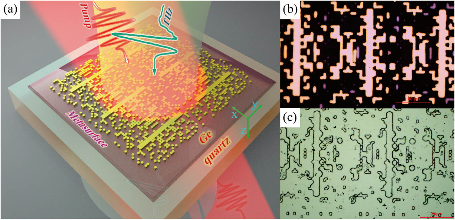
Figure 1.Structure chart of ultrafast all-optical terahertz modulation. (a) Schematic illustration of hybrid structure combining Ge film with inverse-designed metasurface at the pump light of 800 nm for terahertz modulation. (b) Processed inverse-designed metasurface structure without Ge film covering on the face. (c) Processed inverse-designed metasurface structure covering 200 nm thick Ge film on the face. The scale bar in the pictures is 50 μm.
![]()
Figure 2.Sketched scheme of inverse design of ultrafast terahertz modulator based on EIT effect utilizing the PSO algorithm and finite-difference time-domain method. (a) General design cycle of PSO algorithm. At this optimization procedure, we set the target function by using coupled harmonic oscillator model. The number of particles is set as 10, and the number of iterations is 100. (b) The fitness function tends to convergence with the increasing iterations. After 60 iterations, the fitness is convergent, and the result is what we want. (c) The transmittance of the terahertz wave at the last design is described in the red line, and the black line shows the target transmittance. All terahertz transmittance is obtained through finite-difference time-domain method.
B. Light-Activated Germanium-Controlled Terahertz EIT Resonance Switching
To further study the EIT effect caused by our designed metasurface, pump light at wavelength 800 nm (an optical pulse of energy 1.55 eV, which is higher than the energy bandgap of the Ge film) was use to excite photoinduced carrier concentrations of Ge and change its conductivity to modulate the shape of the EIT spectrum as shown in Fig. 3. Due to the high sensitivity to the electromagnetic environment, EIT resonance can switch on or off at different pumping energy fluences. Figure 3(a) displays the experimental transmission spectral dispersion of a hybrid structure combined with Ge film and a metasurface at various pumping energy fluences. Optical excitation of Ge film results in interband transition of electrons from the valence band to the conduction band. The injected free carriers give rise to the changes of local electromagnetic environment and lead to different coupled strength between the bright mode and dark mode. In other words, the free carriers of photoexcited Ge film alter the strength of terahertz electric field confined in our inverse-designed metasurface structure. This change generates a strong modulation of EIT resonance amplitude. With the optical pump energy fluence increasing from 0 to , the EIT resonance (defined by a transmittance peak at 0.76 THz and dip at 0.67 THz) is increasingly suppressed as the concentration of photoexcited free carriers increases. The transmission resonance amplitude defined by achieves maximum with no pump light and decreases with growing pump energy fluence. The normalized resonance amplitude extracted from transmittance spectra is shown in Fig. 3(b), reaching over 95% modulation depth in our experiment. All results show the trend toward smoothness with the resonance being almost completely faded away at pump energy over . On the other hand, our simulation results described in Figs. 3(c) and 3(d) show the same trend as the experimental process. By changing the conductivity of Ge film covered over the inverse-designed metasurface, the local electromagnetic environment alters and contributes to modulation of terahertz wave information including amplitude and phase. In this work, we define the state of “switching on” at the maximal resonance amplitude and the state of “switching off” at the case of over 90% modulation of normalized resonance amplitude. In the simulation, we set the corresponding conductivities for references only to illustrate the tendency of EIT modulation [29]. With the conductivity of Ge film ranging from (without pump) to (with high pump power), the EIT resonance amplitude falls to zeros gradually. It is clear that the EIT resonance is eliminated with the conductivity of Ge up to , meaning in the switched-off state. Note that the resonance frequency in our experiment is different from the simulation. (The transmission peak of EIT is 0.79 THz in our simulation, and the dip is 0.57 THz.) The depth of EIT resonance also has distinction. Mainly, we attribute these differences of transmittance spectra between experiment and simulation (the structure we simulated is from inverse design) to the fabrication errors and the material characters. Another significant physical phenomenon based on EIT is the slow-light effect that is described in Fig. 7 (Appendix A). Without loss of generality, we quantitatively characterize the slow-light performance in our inverse-designed hybrid metasurface structure combined with Ge film as the group delay , where is the terahertz angle frequency. As we can see, the group delay influenced by the slow-light phenomenon of the EIT effect reaches 1.65 ps at a certain frequency 0.76 THz (the peak of transmittance spectra of the EIT window) without pump light. Subsequently, the slow-light effect degrades together with the increasing pump fluence, presenting as the group delay at the peak of the transparency window trending to 0 ps. Both optical excited modulation of transmittance amplitude and the slow-light effect reveal, in a way, that EIT effect exists in our inverse-designed metasurface structure, offering a high sensitivity for carrying out THz modulation.
![]()
Figure 3.Experimentally light-activated Ge-controlled terahertz EIT modulation for varying pump fluences and simulation results of EIT resonance modulation with different conductivities of Ge film. (a) Experimental modulation of terahertz EIT amplitudes for various pump fluences ranging from 0 to
C. Ultrafast Dynamics of EIT Resonance Amplitude Modulation
The ongoing request is to investigate the dynamically tunable terahertz EIT response of a hybrid structure integrating an inverse-designed metasurface with Ge film. By taking advantage of optical pump terahertz probe (OPTP) technology, we explore the possibility of the ultrafast switch dynamics for terahertz EIT resonance. As just mentioned before, the modulation behavior can be influenced by optical pump excitation, together with Ge carrier dynamics changing in the time domain. Therefore, by moving the pump-probe delay stage, we employ the time-resolved optical pump measurements to illustrate the ultrafast modulation processes at a selectable optical pump fluence of , where the largest modulation depth can come true. The time delay given in Fig. 4 represents the relative time delay in the arrival of the pump light and the terahertz probe at the sample face. The time-domain terahertz spectra are experimentally measured by a terahertz time-domain spectrum (TDS) system for each relative time delay, and then the dynamics of terahertz modulation can be exhibited. First, we characterize the ultrafast relaxation time of the pure Ge film with femtosecond pulse laser pumping, which is shown in Fig. 8 (Appendix A). Depending on different carrier concentrations in time scale, the absolute transmission change defined by was measured by OPTP, where is the transmission of a terahertz pulse through the sample at a real time, and is that of the sample in absence of pump fluence. To improve the signal-to-noise ratio, we set the time delay of TDS at the maximum amplitude of terahertz pulse in the time domain to explore the terahertz transmittance. The negative differential transmission of pure Ge film exhibits a characteristic curve performed by an exponential delay. The mono-exponential delay profiles convolved with the instrument response function can be used to fit the experimentally measured results, given by [62]
![]()
Figure 4.Temporal evolution dynamics of ultrafast terahertz modulation behaviors under the pump fluence
D. Near-Field Distributions of Inverse-Designed Metasurface Combined with Ge Film
In order to illuminate the physical mechanism of terahertz EIT modulation of the inverse-designed metasurface with Ge film, we perform the simulations of near-field distributions as a function of the conductivity of Ge film. To clarify the interaction between dark mode and bright mode, a field profile monitor monitoring the near field at 0.67 THz (the dip of transmittance spectra of EIT resonance) is placed 1 μm above the metasurface. It is visible that the near-field radiation of the metasurface entirety gradually decreases as shown in Figs. 5(a)–5(d), with increasing conductivity of Ge film from 10 to 1000 S/m. More details discovered in the near-field profiles show that the electric field distribution of cut wire nearly keeps unchanged with the increased conductivity of Ge film and performs a dipole resonance. Then the dipole resonance can reradiate the terahertz wave and play a role in bright mode in the EIT effect. In contrast to the cut wire in the metasurface, the near-field strength of the nearby cross group is higher, and weakens with growing conductivity of the Ge film. We consider these modes dark modes due to the strong confinement of electric field in the crosses. The increasing conductivity of Ge film reduces the strength of dark modes and meanwhile weakens the interaction between bright mode and dark mode, allowing for gradually declining EIT resonance amplitude. The tendency of EIT modulation in our experiment through various pump fluences is in accord with the transformation of near-field strength in simulation with different conductivities of Ge film.
![]()
Figure 5.Simulated near-field distributions as a function of Ge film conductivity ranging from 10 to 1000 S/m.
![]()
Figure 6.(a) Schematic illustration of one-unit inverse-designed metasurface combined with 200 nm thick Ge film (the red part), including a cut wire and numerous crosses around it. The material of inverse-designed metasurface is gold with thickness of 200 nm (the golden part). The whole unit structure is mirror symmetric. The periods of one-unit metasurface are
![]()
Figure 7.Experimentally measured group delay spectra of hybrid structure combining a reverse-designed metasurface with Ge film as a function of pump fluence ranging from 0 to
![]()
Figure 8.Negative differential transmission spectra of pure 200 nm thick Ge film are experimentally measured at the maximal amplitude of terahertz time-domain pulse signal as a function of optical-pump terahertz time delay. Experimental data points are fitted with equation in the main text and the delay time constants
![]()
Figure 9.Modulations of the EIT resonance amplitude as a function of pump-probe time delay evaluated from the transmission spectra of Fig.
3. CONCLUSION
In summary, using a PSO algorithm, we have performed an inverse-designed metasurface supporting the EIT effect. Through setting a goal fitness calculated by a coupled harmonic oscillator model, we search for the terahertz transmittance displaying a desired EIT window, and then we manufacture this inverse-designed structure so as to experimentally find the EIT effect, which confirmed a feasible scheme to design ultrasensitive terahertz physics phenomena. Utilizing its sensitive character, we further verify this EIT effect by covering Ge film in the structure and optical excitation realizes modulation of EIT resonance amplitude as well as slow-light switching. Furthermore, under the pump pulse excitation, dynamical modulation of this Ge film hybrid metasurface exhibits ultrafast switching characteristic in the picosecond time scale. Also, the near-field profiles from simulation confirm the interaction between bright mode and dark mode at various conductivity of Ge film, agreeing well with the modulation of terahertz EIT resonance amplitude at different pump energy densities. Compared to split ring resonators and other conventional metamaterial structures, the inverse-designed structure in the terahertz regime provides a more flexible method to design multifunctional terahertz devices. In the future, the optimization algorithm of inverse design could be extended to incorporate interesting physics and modulators such as multiple EIT resonance modulation and broadband polarization converters. Our results suggest that this method is useful for terahertz modulation and paves the way for advanced terahertz multifunction devices with high performance.
APPENDIX A
References
[1] M. Tonouchi. Cutting-edge terahertz technology. Nat. Photonics, 1, 97-105(2007).
[2] S. Koenig, D. Lopez-Diaz, J. Antes, F. Boes, R. Henneberger, A. Leuther, A. Tessmann, R. Schmogrow, D. Hillerkuss, R. Palmer, T. Zwick, C. Koos, W. Freude, O. Ambacher, J. Leuthold, I. Kallfass. Wireless sub-THz communication system with high data rate. Nat. Photonics, 7, 977-981(2013).
[3] X. Zang, W. Xu, M. Gu, B. Yao, L. Chen, Y. Peng, J. Xie, A. V. Balakin, A. P. Shkurinov, Y. Zhu, S. Zhuang. Polarization-insensitive metalens with extended focal depth and longitudinal high-tolerance imaging. Adv. Opt. Mater., 8, 1901342(2020).
[4] S. Zhong. Progress in terahertz nondestructive testing: a review. Front. Mech. Eng., 14, 273-281(2019).
[5] Y. Kawano. Terahertz sensing and imaging based on nanostructured semiconductors and carbon materials. Laser Photon. Rev., 6, 246-257(2012).
[6] P. U. Jepsen, D. G. Cooke, M. Koch. Terahertz spectroscopy and imaging–Modern techniques and applications. Laser Photon. Rev., 5, 124-166(2011).
[7] Y. Hu, T. Jiang, J. Zhou, H. Hao, H. Sun, H. Ouyang, M. Tong, Y. Tang, H. Li, J. You, X. Zheng, Z. Xu, X. Cheng. Ultrafast terahertz frequency and phase tuning by all-optical molecularization of metasurfaces. Adv. Opt. Mater., 7, 1970084(2019).
[8] T. Nagatsuma, G. Ducournau, C. C. Renaud. Advances in terahertz communications accelerated by photonics. Nat. Photonics, 10, 371-379(2016).
[9] X. C. Q. Yang, Q. Xu, C. Tian, Y. Xu, L. Cong, X. Zhang, Y. Li, C. Zhang, X. Zhang, J. Han, W. Zhang. Broadband terahertz rotator with an all-dielectric metasurface. Photon. Res., 6, 1056-1061(2018).
[10] Z. Chen, X. Chen, L. Tao, K. Chen, M. Long, X. Liu, K. Yan, R. I. Stantchev, E. Pickwell-MacPherson, J. B. Xu. Graphene controlled Brewster angle device for ultra broadband terahertz modulation. Nat. Commun., 9, 4909(2018).
[11] L. Cong, Y. K. Srivastava, H. Zhang, X. Zhang, J. Han, R. Singh. All-optical active THz metasurfaces for ultrafast polarization switching and dynamic beam splitting. Light Sci. Appl., 7, 28(2018).
[12] C. C. Chang, Z. Zhao, D. Li, A. J. Taylor, S. Fan, H. T. Chen. Broadband linear-to-circular polarization conversion enabled by birefringent off-resonance reflective metasurfaces. Phys. Rev. Lett., 123, 237401(2019).
[13] H.-T. Chen, W. J. Padilla, J. M. O. Zide, A. C. Gossard, A. J. Taylor, R. D. Averitt. Active terahertz metamaterial devices. Nature, 444, 597-600(2006).
[14] Z. Miao, Q. Wu, X. Li, Q. He, K. Ding, Z. An, Y. Zhang, L. Zhou. Widely tunable terahertz phase modulation with gate-controlled graphene metasurfaces. Phys. Rev. X, 5, 041027(2015).
[15] H.-T. Chen, J. F. O’Hara, A. K. Azad, A. J. Taylor, R. D. Averitt, D. B. Shrekenhamer, W. J. Padilla. Experimental demonstration of frequency-agile terahertz metamaterials. Nat. Photonics, 2, 295-298(2008).
[16] S. J. Kindness, N. W. Almond, B. Wei, R. Wallis, W. Michailow, V. S. Kamboj, P. Braeuninger-Weimer, S. Hofmann, H. E. Beere, D. A. Ritchie, R. Degl’Innocenti. Active control of electromagnetically induced transparency in a terahertz metamaterial array with graphene for continuous resonance frequency tuning. Adv. Opt. Mater., 6, 1800570(2018).
[17] S. Xiao, T. Wang, T. Liu, X. Yan, Z. Li, C. Xu. Active modulation of electromagnetically induced transparency analogue in terahertz hybrid metal-graphene metamaterials. Carbon, 126, 271-278(2018).
[18] S. Han, L. Cong, Y. K. Srivastava, B. Qiang, M. V. Rybin, A. Kumar, R. Jain, W. X. Lim, V. G. Achanta, S. S. Prabhu, Q. J. Wang, Y. S. Kivshar, R. Singh. All-dielectric active terahertz photonics driven by bound states in the continuum. Adv. Mater., 31, 1901921(2019).
[19] L. Cong, R. Singh. Symmetry-protected dual bound states in the continuum in metamaterials. Adv. Opt. Mater., 7, 1900383(2019).
[20] M. Liu, Z. Tian, X. Zhang, J. Gu, C. Ouyang, J. Han, W. Zhang. Tailoring the plasmon-induced transparency resonances in terahertz metamaterials. Opt. Express, 25, 19844-19855(2017).
[21] X. Chen, S. Ghosh, Q. Xu, C. Ouyang, Y. Li, X. Zhang, Z. Tian, J. Gu, L. Liu, A. K. Azad, J. Han, W. Zhang. Active control of polarization-dependent near-field coupling in hybrid metasurfaces. Appl. Phys. Lett., 113, 061111(2018).
[22] J. Gu, R. Singh, X. Liu, X. Zhang, Y. Ma, S. Zhang, S. A. Maier, Z. Tian, A. K. Azad, H.-T. Chen, A. J. Taylor, J. Han, W. Zhang. Active control of electromagnetically induced transparency analogue in terahertz metamaterials. Nat. Commun., 3, 1151(2012).
[23] T.-T. Kim, H.-D. Kim, R. Zhao, S. S. Oh, T. Ha, D. S. Chung, Y. H. Lee, B. Min, S. Zhang. Electrically tunable slow light using graphene metamaterials. ACS Photon., 5, 1800-1807(2018).
[24] Y. Hu, T. Jiang, J. Zhou, H. Hao, H. Sun, H. Ouyang, M. Tong, Y. Tang, H. Li, J. You, X. Zheng, Z. Xu, X. Cheng. Ultrafast terahertz transmission/group delay switching in photoactive WSe2-functionalized metaphotonic devices. Nano Energy, 68, 104280(2020).
[25] Y. K. Srivastava, A. Chaturvedi, M. Manjappa, A. Kumar, G. Dayal, C. Kloc, R. Singh. MoS2 for ultrafast all-optical switching and modulation of THz Fano metaphotonic devices. Adv. Opt. Mater., 5, 1700762(2017).
[26] A. Kumar, A. Solanki, M. Manjappa, S. Ramesh, Y. K. Srivastava, P. Agarwal, T. C. Sum, R. Singh. Excitons in 2D perovskites for ultrafast terahertz photonic devices. Sci. Adv., 6, eaax8821(2020).
[27] M. Manjappa, Y. K. Srivastava, A. Solanki, A. Kumar, T. C. Sum, R. Singh. Hybrid lead halide perovskites for ultrasensitive photoactive switching in terahertz metamaterial devices. Adv. Mater., 29, 1605881(2017).
[28] Y. Hu, J. You, M. Tong, X. Zheng, Z. Xu, X. Cheng, T. Jiang. Pump-color selective control of ultrafast all-optical switching dynamics in metaphotonic devices. Adv. Sci., 7, 2000799(2020).
[29] W. X. Lim, M. Manjappa, Y. K. Srivastava, L. Cong, A. Kumar, K. F. MacDonald, R. Singh. Ultrafast all-optical switching of germanium-based flexible metaphotonic devices. Adv. Mater., 30, 1705331(2018).
[30] H. J. Joyce, J. L. Boland, C. L. Davies, S. A. Baig, M. B. Johnston. A review of the electrical properties of semiconductor nanowires: insights gained from terahertz conductivity spectroscopy. Semicond. Sci. Technol., 31, 103003(2016).
[31] J. S. Jensen, O. Sigmund. Topology optimization for nano-photonics. Laser Photon. Rev., 5, 308-321(2011).
[32] M. Minkov, I. A. D. Williamson, L. C. Andreani, D. Gerace, B. Lou, A. Y. Song, T. W. Hughes, S. Fan. inverse design of photonic crystals through automatic differentiation. ACS Photon., 7, 1729-1741(2020).
[33] D. Sell, J. Yang, S. Doshay, R. Yang, J. A. Fan. Large-angle, multifunctional metagratings based on freeform multimode geometries. Nano Lett., 17, 3752-3757(2017).
[34] C. Sitawarin, W. Jin, Z. Lin, A. W. Rodriguez. Inverse-designed photonic fibers and metasurfaces for nonlinear frequency conversion [invited]. Photon. Res., 6, B82-B89(2018).
[35] W. Ma, F. Cheng, Y. Xu, Q. Wen, Y. Liu. Probabilistic representation and inverse design of metamaterials based on a deep generative model with semi-supervised learning strategy. Adv. Mater., 31, 1901111(2019).
[36] Y. Chen, Y. Hu, J. Zhao, Y. Deng, Z. Wang, X. Cheng, D. Lei, Y. Deng, H. Duan. Topology optimization-based inverse design of plasmonic nanodimer with maximum near-field enhancement. Adv. Funct. Mater., 30, 2000642(2020).
[37] A. Y. Piggott, J. Lu, K. G. Lagoudakis, J. Petykiewicz, T. M. Babinec, J. Vučković. Inverse design and demonstration of a compact and broadband on-chip wavelength demultiplexer. Nat. Photonics, 9, 374-377(2015).
[38] L. Su, A. Y. Piggott, N. V. Sapra, J. Petykiewicz, J. Vučković. Inverse design and demonstration of a compact on-chip narrowband three-channel wavelength demultiplexer. ACS Photon., 5, 301-305(2018).
[39] B. Shen, P. Wang, R. Polson, R. Menon. An integrated-nanophotonics polarization beamsplitter with 2.4 × 2.4 μm2 footprint. Nat. Photonics, 9, 378-382(2015).
[40] S. Y. Y. Zhang, A. E.-J. Lim, G.-Q. Lo, C. Galland, T. Baehr-Jones, M. Hochberg. A compact and low loss Y-junction for submicron silicon waveguide. Opt. Express, 21, 1310-1316(2013).
[41] B. Shen, P. Wang, R. Polson, R. Menon. Ultra-high-efficiency metamaterial polarizer. Optica, 1, 356-360(2014).
[42] S. So, T. Badloe, J. Noh, J. Rho, J. Bravo-Abad. Deep learning enabled inverse design in nanophotonics. Nanophotonics, 9, 1041-1057(2020).
[43] S. Molesky, Z. Lin, A. Y. Piggott, W. Jin, J. Vucković, A. W. Rodriguez. Inverse design in nanophotonics. Nat. Photonics, 12, 659-670(2018).
[44] L. Su, D. Vercruysse, J. Skarda, N. V. Sapra, J. A. Petykiewicz, J. Vučković. Nanophotonic inverse design with SPINS: software architecture and practical considerations. Appl. Phys. Rev., 7, 011407(2020).
[45] W. Ma, F. Cheng, Y. Liu. Deep-learning-enabled on-demand design of chiral metamaterials. ACS Nano, 12, 6326-6334(2018).
[46] M. D. Huntington, L. J. Lauhon, T. W. Odom. Subwavelength lattice optics by evolutionary design. Nano Lett., 14, 7195-7200(2014).
[47] Z. Lin, X. Liang, M. Lončar, S. G. Johnson, A. W. Rodriguez. Cavity-enhanced second-harmonic generation via nonlinear-overlap optimization. Optica, 3, 233-238(2016).
[48] J. C. Mak, C. Sideris, J. Jeong, A. Hajimiri, J. K. Poon. Binary particle swarm optimized 2 x 2 power splitters in a standard foundry silicon photonic platform. Opt. Lett., 41, 3868-3871(2016).
[49] T. Nakanishi, Y. Nakata, Y. Urade, K. Okimura. Broadband operation of active terahertz quarter-wave plate achieved with vanadium-dioxide-based metasurface switchable by current injection. Appl. Phys. Lett., 117, 091102(2020).
[50] D. Wang, L. Zhang, Y. Gong, L. Jian, T. Venkatesan, C. Qiu, M. Hong. Multiband switchable terahertz quarter-wave plates via phase-change metasurfaces. IEEE Photon. J., 8, 5500308(2016).
[51] D. Wang, L. Zhang, Y. Gu, M. Q. Mehmood, Y. Gong, A. Srivastava, L. Jian, T. Venkatesan, C.-W. Qiu, M. Hong. Switchable ultrathin quarter-wave plate in terahertz using active phase-change metasurface. Sci. Rep., 5, 15020(2015).
[52] M. Manjappa, A. Solanki, A. Kumar, T. C. Sum, R. Singh. Solution-processed lead iodide for ultrafast all-optical switching of terahertz photonic devices. Adv. Mater., 31, 1901455(2019).
[53] S. Zhang, D. A. Genov, Y. Wang, M. Liu, X. Zhang. Plasmon-induced transparency in metamaterials. Phys. Rev. Lett., 101, 047401(2008).
[54] P. Tassin, L. Zhang, R. Zhao, A. Jain, T. Koschny, C. M. Soukoulis. Electromagnetically induced transparency and absorption in metamaterials: the radiating two-oscillator model and its experimental confirmation. Phys. Rev. Lett., 109, 187401(2012).
[55] R. Eberhart, J. Kennedy. A new optimizer using particle swarm theory. Proceedings of the Sixth International Symposium on Micro Machine and Human Science (MHS’95), 39-43(1995).
[56] D.-C. Wang, R. Tang, Z. Feng, S. Sun, S. Xiao, W. Tan. Symmetry-assisted spectral line shapes manipulation in dielectric double-Fano metasurfaces. Adv. Opt. Mater., 9, 2001874(2021).
[57] D.-C. Wang, S. Sun, Z. Feng, W. Tan, C.-W. Qiu. Multipolar-interference-assisted terahertz waveplates via all-dielectric metamaterials. Appl. Phys. Lett., 113, 201103(2018).
[58] T. W. Hughes, M. Minkov, I. A. D. Williamson, S. Fan. Adjoint method and inverse design for nonlinear nanophotonic devices. ACS Photon., 5, 4781-4787(2018).
[59] Z. Tao, J. You, J. Zhang, X. Zheng, H. Liu, T. Jiang. Optical circular dichroism engineering in chiral metamaterials utilizing a deep learning network. Opt. Lett., 45, 1403-1406(2020).
[60] Z. Tao, J. Zhang, J. You, H. Hao, H. Ouyang, Q. Yan, S. Du, Z. Zhao, Q. Yang, X. Zheng, T. Jiang. Exploiting deep learning network in optical chirality tuning and manipulation of diffractive chiral metamaterials. Nanophotonics, 9, 2945-2956(2020).
[61] S. Du, J. You, J. Zhang, Z. Tao, H. Hao, Y. Tang, X. Zheng, T. Jiang. Expedited circular dichroism prediction and engineering in two-dimensional diffractive chiral metamaterials leveraging a powerful model-agnostic data enhancement algorithm. Nanophotonics, 10, 20200570(2020).
[62] M. ElKabbash, A. R. Rashed, B. Kucukoz, Q. Nguyen, A. Karatay, G. Yaglioglu, E. Ozbay, H. Caglayan, G. Strangi. Ultrafast transient optical loss dynamics in exciton–plasmon nano-assemblies. Nanoscale, 9, 6558-6566(2017).

Set citation alerts for the article
Please enter your email address
© Copyright 2018-2021 | Chinese Laser Press. All Rights Reserved 沪ICP备15018463号-20