
Zhicheng Dai, Yushen Liu, Guofeng Yang, Feng Xie, Chun Zhu, Yan Gu, Naiyan Lu, Qigao Fan, Yu Ding, Yuhang Li, Yingzhou Yu, Xiumei Zhang. Carrier transport and photoconductive gain mechanisms of AlGaN MSM photodetectors with high Al Content[J]. Chinese Optics Letters, 2021, 19(8): 082504
- Chinese Optics Letters
- Vol. 19, Issue 8, 082504 (2021)
Abstract
Keywords
1. Introduction
Ultraviolet (UV) photodetectors (PDs) have obtained wide applications in many fields due to their huge advantages, such as superior thermal stability, high sensitivity, and reliability[
As is well known, MSM PD structures consist of two metal electrodes with back-to-back Schottky contact, one in positive contact and the other in reverse bias contact. The ideal MSM PDs with Schottky contact are not expected to exhibit an internal gain, and the responsivity should not change with the applied bias[
Here, we have fabricated an solar-blind MSM PD. The MSM PD possesses high spectral responsivity and external quantum efficiency due to the photoconductive gain mechanism. Furthermore, the dark current and photocurrent of the PD at room and high temperatures are investigated, indicating its excellent working characteristic at high temperature. The Poole–Frenkel emission (PFE) model and changing space charge regions are explored to explain the carrier transport and photoconductive gain mechanisms for high-Al-content solar-blind MSM PDs, respectively.
Sign up for Chinese Optics Letters TOC. Get the latest issue of Chinese Optics Letters delivered right to you!Sign up now
2. Experimental Details
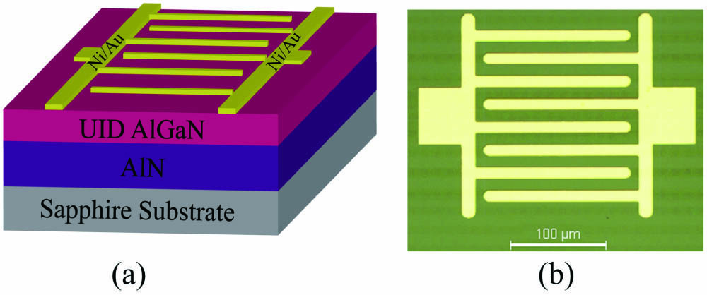
Figure 1(a) illustrates the epitaxial structure of the solar-blind MSM PD. The PD epitaxial layers were grown by metal organic chemical vapor deposition (MOCVD), which consisted of a sapphire substrate, a 1 µm AlN buffer layer, and a 1 µm unintentionally doped (UID) active layer. Figure 1(b) shows an optical microscopy image of the fabricated AlGaN PD. To form two back-to-back Schottky contact electrodes, 50 nm Ni and 100 nm Au metal stacks were fabricated on the surface of the active layer by electron beam (EB) evaporation, and eight sets of interdigital electrodes with a length of 200 µm were formed. The widths and the spacings of the interdigital electrodes were both 12 µm. The contact electrodes were annealed at 250°C for 120 s through rapid thermal annealing in a environment.
![]()
Figure 1.(a) Epitaxial structure of the Al0.55Ga0.45N solar-blind MSM PD. (b) Optical microscopy image of the Al0.55Ga0.45N MSM PD with an area of 200 µm × 200 µm.
The crystal phase and morphology of the epitaxial layer were characterized by atomic force microscopy (AFM) and high-resolution X-ray diffraction (XRD). A transmission electron microscope (TEM) was employed to analyze the dislocations of the layer. Temperature-dependent current–voltage (I-V) curves were characterized by utilizing a Keithley 4200 semiconductor parameter analyzer in dark or under the illumination of 230 nm monochromatic light. The temperature was controlled from 300 K to 425 K on a probe station with a heater. In addition, the spectral responsivity of the PD was measured using a monochromator fitted with a 500 W xenon lamp as the excitation source. The optical power density at different wavelengths was calibrated by a standardized Si-based PD.
3. Results and Discussion
Figure 2(a) displays the omega-2theta XRD pattern of the plane, where the diffraction peaks of the active layer and the AlN buffer layer can be clearly observed. A AFM image of the surface shown in Fig. 2(b) indicates that typical step-flow structures dominate the surface morphology, and the surface root-mean-square (RMS) roughness is 1.02 nm. Figures 2(c) and 2(d) show the dark-field TEM images of the interface, where the AlGaN active layer and the AlN buffer layer are separated by the green dashed line. It is estimated from the TEM images that the screw dislocation density is , and the edge dislocation density is for the active layer.
![]()
Figure 2.(a) Omega-2theta XRD pattern of the Al0.55Ga0.45N (002) plane. (b) Typical 5 µm × 5 µm AFM image of the AlGaN epitaxial layer. (c), (d) TEM images of the AlGaN/AlN interface.
Figure 3(a) shows the transmission spectrum of the active layer. A sharp cutoff appears in the transmission spectrum curve around 265 nm with the transmittance reaching 65%, which verifies the Al content of 0.55 in the AlGaN active layer. Figure 3(b) exhibits the spectral response at different bias voltages for the solar-blind MSM PD on a logarithmic scale. It can be seen that the responsivities under different voltages exhibit maximum peaks at about 265 nm with optical power of , which further corresponds to the bandgap of AlGaN with an Al content of 0.55. In addition, assuming that the gain is one, and the external quantum efficiency is 100%, the ideal responsivity expected for MSM PD is 0.21 A/W from[
![]()
Figure 3.(a) Transmission spectrum of Al0.55Ga0.45N active layer. (b) Photo-response spectra of the Al0.55Ga0.45N PD from 2 to 10 V at room temperature on the logarithmic scale.
Figure 4 shows the I-V curves of the PD in dark and under 230 nm UV illumination at 25°C and 150°C. It is observed that the MSM PD has a low dark current of approximately 2.56 nA under a bias voltage of 2 V. In addition, the specific detectivity ratio () under weak signals is an important indicator for evaluating the comprehensive performance of PDs and can be determined by[
![]()
Figure 4.I-V curves of the Al0.55Ga0.45N MSM PD in the dark and under 230 nm illumination at 25°C and 150°C. The inset is the breakdown voltage of the PD.
In order to study the carrier transport mechanism of the high-Al-content MSM PD, the I-V characteristics measured under different temperatures are depicted in Fig. 5. It is found that when the bias voltage is less than 4 V, the curves of the reverse leakage current at different temperatures basically overlap, indicating that the leakage current exhibits weak dependence on the temperature at low bias voltage, which demonstrates that the tunneling effect is the dominant origin of leakage current flow[
![]()
Figure 5.Temperature-dependent I-V characteristics of the Al0.55Ga0.45N MSM PD in dark conditions.
It is well known that the current related to PFE is expressed as[
![]()
Figure 6.(a) Derived ln(IPF/E) versus sqrt(E) curves employing PFE as carrier transport mechanism at high bias voltages. (b) Derived linear fit of parameter m(T) versus q/kT. (c) Linear fit of parameter n(T) versus q/kT. (d) Schematic drawing of the energy band of the metal/AlGaN interface.
As discussed above, the high internal gain existing in the MSM PD is proposed to be caused by photoconductive gain. Here, we adopted the model of space charge region change inside the semiconductor to explain the photoconductivity gain. The current responsivity R of this model can be expressed by[
![]()
Figure 7.Band diagram in the cross section of the AlGaN photoconductor. The dashed line represents the contraction of the band bending around the dislocation under UV illumination.
4. Conclusion
In conclusion, high-Al-content solar-blind MSM PDs were fabricated, and they possess high spectral responsivity, external quantum efficiency, and low UV/visible rejection ratios. It also reveals a solar-blind photo-response with a sharp cutoff wavelength at about 265 nm, and high detectivities of Jones and Jones at 25°C and 150°C under a bias voltage of 4 V are obtained. The extremely high external quantum efficiency indicates the photoconductive gain mechanism for the MSM PDs, which is illustrated by the reduction of the depletion region and the increase in the space charge region under UV illumination. Additionally, the I-V characteristics under different voltages and temperatures demonstrate that the carrier transport of the fabricated solar-blind PDs is dominated by the PFE mechanism.
References
[1] D. Y. Guo, K. Chen, S. L. Wang, F. M. Wu, A. P. Liu, C. R. Li, P. G. Li, C. K. Tan, W. H. Tang. Self-powered solar-blind photodetectors based on α/β phase junction of Ga2O3. Phys. Rev. Appl., 13, 024051(2020).
[2] C. H. Zeng, W. K. Lin, T. He, Y. K. Zhao, Y. H. Sun, Q. Cui, X. Zhang, S. L. Lu, X. M. Zhang, Y. M. Xu, M. Kong, B. S. Zhang. Ultraviolet-infrared dual-color photodetector based on vertical GaN nanowire array and graphine. Chin. Opt. Lett., 18, 112501(2020).
[3] X. Y. Zhou, X. Tan, Y. G. Wang, X. B. Song, T. T. Han, J. Li, W. L. Lu, G. D. Gu, S. X. Liang, Y. J. Lu, Z. H. Feng. High-performance 4H-SiC p-i-n ultraviolet avalanche photodiodes with large active area. Chin. Opt. Lett., 17, 090401(2019).
[4] B. Zhao, F. Wang, H. Y. Chen, Y. P. Wang, M. M. Jiang, X. S. Fang, D. X. Zhao. Solar-blind avalanche photodetector based on single ZnO–Ga2O3 core–shell microwire. Nano. Lett., 15, 3988(2015).
[5] J. Yu, C. X. Shan, X. M. Huang, X. W. Zhang, S. P. Wang, D. Z. Shen. ZnO-based ultraviolet avalanche photodetectors. J. Phys. D, 46, 305105(2013).
[6] K. K. Tian, C. S. Chu, J. M. Che, H. Shao, J. Q. Kou, Y. H. Zhang, Z. H. Zhang, T. B. Wei. On the polarization self-screening effect in multiple quantum wells for nitride-based near ultraviolet light-emitting diodes. Chin. Opt. Lett., 17, 122301(2019).
[7] Z. G. Shao, D. J. Chen, Y. L. Liu, H. Lu, R. Zhang, Y. D. Zheng, L. Li, K. X. Dong. Significant performance improvement in AlGaN solar-blind avalanche photodiodes by exploiting the built-in polarization electric field. IEEE J. Sel. Top. Quantum Electron., 20, 3803306(2014).
[8] E. Monroy, F. Calle, J. A. Garrido, P. Youinou, E. Muñoz, F. Omnès, B. Beaumont, P. Gibart. Si-doped AlxGa1-xN photoconductive detectors. Semicond. Sci. Technol., 14, 685(1999).
[9] H. Jiang, N. Nakata, G. Y. Zhao, H. Ishikawa, C. L. Shao, T. Egawa, T. Jimbo, M. Umeno. Back-illuminated GaN metal-semiconductor-metal UV photodetector with high internal gain. Jpn. J. Appl. Phys., 40, L505(2001).
[10] S. Walde, M. Brendel, U. Zeimer, F. Brunner, S. Hagedorn, M. Weyers. Impact of open-core threading dislocations on the performance of AlGaN metal-semiconductor-metal photodetectors. J. Appl. Phys., 123, 161551(2018).
[11] F. Xie, H. Lu, D. J. Chen, P. Han, R. Zhang, Y. D. Zheng, L. Li, W. H. Jiang, C. Chen. Large-area solar-blind AlGaN-based MSM photodetectors with ultra-low dark current. Electron. Lett., 47, 930(2011).
[12] O. Katz, V. Garber, B. Meyler, G. Bahir, J. Salzman. Gain mechanism in GaN Schottky ultraviolet detectors. Appl. Phys. Lett., 79, 1417(2001).
[13] Y. Xu, X. H. Chen, D. Zhou, F. F. Ren, J. J. Zhou, S. Bai, H. Lu, S. Gu, R. Zhang, Y. D. Zheng, J. D. Ye. Carrier transport and gain mechanisms in β–Ga2O3-based metal–semiconductor–metal solar-blind Schottky photodetectors. IEEE Trans. Electron Devices, 66, 2276(2019).
[14] H. Srour, J. P. Salvestrini, A. Ahaitouf, S. Gautier, T. Moudakir, B. Assouar, M. Abarkan, S. Hamady, A. Ougazzaden. Solar blind metal-semiconductor-metal ultraviolet photodetectors using quasi-alloy of BGaN/GaN superlattices. Appl. Phys. Lett., 99, 221101(2011).
[15] O. Katz, G. Bahir, J. Salzman. Persistent photocurrent and surface trapping in GaN Schottky ultraviolet detectors. Appl. Phys. Lett., 84, 4092(2004).
[16] D. B. Li, X. J. Sun, H. Song, Z. M. Li, Y. R. Chen, G. Q. Miao, H. Jiang. Influence of threading dislocations on GaN-based metal-semiconductor-metal ultraviolet photodetectors. Appl. Phys. Lett., 98, 1541(2011).
[17] P. K. Rao, B. Park, S. T. Lee, Y. K. Noh, M. D. Kim, J. E. Oh. Analysis of leakage current mechanisms in Pt/Au Schottky contact on Ga-polarity GaN by Frenkel–Poole emission and deep level studies. J. Appl. Phys., 110, 013716(2011).
[18] B. S. Simpkins, E. T. Yu, P. Waltereit, J. S. Speck. Correlated scanning Kelvin probe and conductive atomic force microscopy studies of dislocations in gallium nitride. J. Appl. Phys., 94, 1448(2003).
[19] S. Rathkanthiwar, A. Kalra, S. V. Solanke, N. Mohta, R. Muralidharan, S. Raghavan, D. N. Nath. Gain mechanism and carrier transport in high responsivity AlGaN-based solar blind metal semiconductor metal photodetectors. J. Appl. Phys., 121, 164502(2017).
[20] E. Monroy, F. Calle, E. Munoz, F. Omnès, B. Beaumont, P. Gibart. Visible-blindness in photoconductive and photovoltaic AlGaN ultraviolet detectors. J. Electron. Mater., 28, 240(1999).
[21] N. Youngblood, C. Chen, S. J. Koester, M. Li. Waveguide-integrated black phosphorus photodetector with high responsivity and low dark current. Nat. Photon., 9, 247(2015).
[22] X. K. Zhou, D. Z. Yang, D. G. Ma, A. Vadim, T. Ahamad, S. M. Alshehri. Ultrahigh gain polymer photodetectors with spectral response from UV to near‐infrared using ZnO nanoparticles as anode interfacial layer. Adv. Funct. Mater., 26, 6619(2016).
[23] H. Zhang, E. J. Miller, E. T. Yu. Analysis of leakage current mechanisms in Schottky contacts to GaN and Al0.25Ga0.75N/GaN grown by molecular-beam epitaxy. J. Appl. Phys., 99, 023703(2006).
[24] F. C. Chiu. A review on conduction mechanisms in dielectric films. Adv. Mater. Sci. Eng., 2014, 578168(2014).
[25] E. Arslan, S. Buetuen, E. Ozbay. Leakage current by Frenkel–Poole emission in Ni/Au Schottky contacts on Al0.83In0.17N/AlN/GaN heterostructures. Appl. Phy. Lett., 94, 142106(2009).
[26] J. R. Yeargan, H. L. Taylor. The Poole–Frenkel effect with compensation present. J. Appl. Phys., 39, 5600(1968).
[27] V. W. L. Chin, T. L. Tansley, T. Osotchan. Electron mobilities in gallium, indium, and aluminum nitrides. J. Appl. Phys., 75, 7365(1994).
[28] O. Ambacher, J. Majewski, C. Miskys, A. Link, M. Hermann, M. Eickhoff, M. Stutzmann, F. Bernardini, V. Fiorentini, V. Tilak. Pyroelectric properties of Al(In)GaN/GaN hetero- and quantum well structures. J. Phys. Condens. Matter, 14, 3399(2002).

Set citation alerts for the article
Please enter your email address
© Copyright 2018-2021 | Chinese Laser Press. All Rights Reserved 沪ICP备15018463号-20