
Chunyan Jin, Wei Wu, Lei Cao, Bofeng Gao, Jiaxin Chen, Wei Cai, Mengxin Ren, Jingjun Xu. Fabrication of lithium niobate metasurfaces via a combination of FIB and ICP-RIE[J]. Chinese Optics Letters, 2022, 20(11): 113602
- Chinese Optics Letters
- Vol. 20, Issue 11, 113602 (2022)
Abstract
1. Introduction
Lithium niobate (, LN) is a key crystal material in photonics, which has comprehensive functional properties, such as optical harmonic generation, electro-optic, acousto-optic, and photorefractive properties[
Until now, there are two main technical routes developed to fabricate the LN metasurfaces. One method is the focused ion beam (FIB) milling[
The FIB milling process, which realizes the nano-structures by direct milling through the LN film using the ion beam (such as gallium ion, ), has several advantages. For example, the FIB milling technique has greater flexibility and lower cost compared with the combined EBL-PE processes. Moreover, the surface and sidewalls of the nano-structures fabricated by the FIB are generally smooth. However, several problems also arise from FIB milling, such as a round top in nano-structures and crystal lattice damage. The first problem could be attributed to angle divergence and scattering of the ion beams and also the redeposition of sputtered atoms during FIB milling. Furthermore, in order to remove the surface lattice damage, amorphization by the high-energy ion beam bombardment and unwanted ion implantation, a subsequent wet treatment by dilute hydrofluoric acid (HF) is usually adopted[
Sign up for Chinese Optics Letters TOC. Get the latest issue of Chinese Optics Letters delivered right to you!Sign up now
On the other hand, the combined EBL-PE process involves first patterning a high-precision electron beam resist (e-beam resist) mask by EBL and then further transferring it to the LN layer by PE. However, LN is chemically inert and therefore difficult to etch. The e-beam resist mask usually has low selectivity to LN, so thick resist is normally required, however, this will greatly limit fabrication resolution and pattern density. Alternatively, multilayer masking schemes have been developed, such as stacking multiple e-beam resist layers or adding hard mask layers [e.g., nickel[
In this paper, to overcome the respective constraints of the above individual technique, we demonstrate a technical route that combines the FIB direct milling and the PE procedure (inductively coupled plasma reactive ion etching, ICP-RIE) to fabricate LN metasurfaces. Unlike the round shaped ridges fabricated by FIB alone, the cross sections obtained here are trapezoids with sidewall angles of larger than 80°. The transmission spectral properties of the metasurfaces are studied both numerically and experimentally. Quasi-bound states in the continuum (QBIC) are steadily observed in experiments, confirming the high quality of the fabricated samples. Our study opens up a new route for fabricating high--factor LN metasurfaces for applications in optical communications, on-chip photonics, laser physics, and sensing.
2. Fabrication of LN Metasurfaces
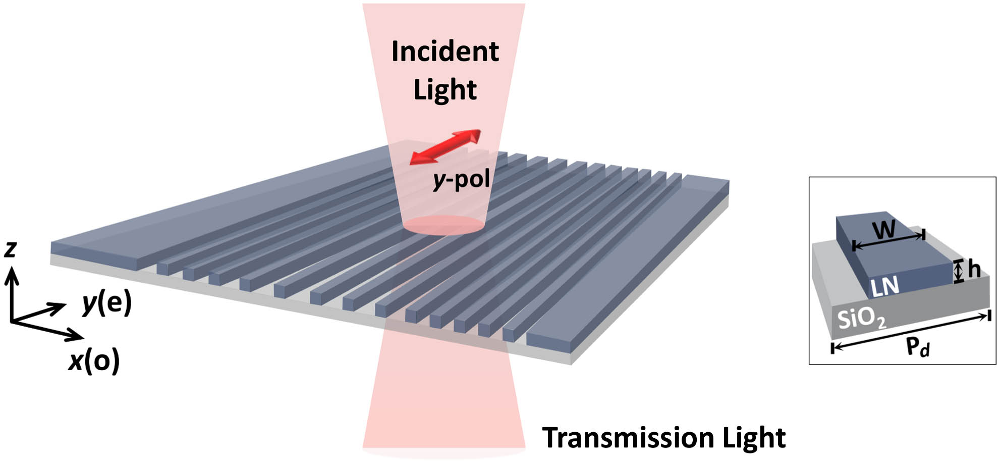
The structural design of the LN nano-grating metasurfaces is illustrated in Fig. 1. The LNOI wafer (NANOLN Co., Ltd.) adopted here includes a quartz substrate and a 230-nm-thick LN film on top. The geometry of the nano-grating array is defined by the ridge width () and the ridge height (). Furthermore, the lattice constant is Pd. Nano-grating ridges are oriented parallel to the optical axis of the LN crystal, denoted here as the axis.
![]()
Figure 1.Schematic of LN nano-grating metasurfaces fabricated on an LNOI wafer. The grating ridges are oriented parallelly to the optical axis of the LN [y(e)]. Geometries of the metasurfaces are defined by period Pd, ridge width w, and height h.
The process to fabricate the metasurfaces is illustrated in Fig. 2(a). In order to remove particles and organic impurities on the surface, the LNOI wafer was first washed with acetone and then rinsed with isopropanol. The entire cleaning process was conducted in an ultrasonic bath. A 40-nm-thick Cr layer, acting as a conducting layer for FIB milling, was further deposited on the LN surface by electron beam evaporation. The good electronic conductivity of the Cr layer ensures a controllable and precise FIB fabrication. Both the Cr and LN layers were milled through and patterned into the nano-grating arrays by the ion beam with a current of 80 pA at an acceleration voltage of 30 kV. The patterned Cr layer served as a protective hard mask in the subsequent ICP-RIE process. This PE process employed a reactive sulfur hexafluoride () gas mixed with physical bombardment argon (Ar) gas. Since the etching rate of the Cr layer is much lower than that of the LN layer, the sidewalls of the LN nano-grating ridges that were unprotected by the Cr mask were selectively etched, and the LN damaged layer and redeposited layer caused by the ion beam were removed as well. The sample was further wet treated using the standard clean 1 (SC-1; by volume) for 5 min at a temperature of 80°C to remove lithium fluoride (LiF), which is a chemical by-product of fluorine-based gas and LN generated during the PE process[
![]()
Figure 2.Illustration of fabrication process. (a) Flow chart: LNOI substrate was cleaned by organic solvent, and a 40-nm-thick Cr layer was deposited on top of the LNOI by electron beam evaporation. Both the Cr and LN layers were milled by FIB followed by an ICP-RIE process. The fabricated structures were treated afterwards by SC-1 solution to remove LiF. Finally, the Cr mask was removed by wet etching. (b) Representative scanning electron microscopy (SEM) images of the fabricated metasurface with Pd = 400 nm. The cross sections are shown on the right, in which Pt is used as a protection layer for cross-section cutting.
Figure 2(b) gives representative scanning electron microscopy (SEM) images of the metasurface with Pd = 400 nm, where the grating duty cycle defined by w/Pd was fixed at 62.5%. In our experiment, a series of tests were performed, and fabricating parameters were determined carefully to ensure the desired duty cycle. The footprint of the metasurface array was . The SEM image in the right panel demonstrates the cross section of the LN nano-ridge, which is an isosceles trapezoid with a top width of 211 nm and a bottom width of 275 nm, hence a slant angle of about 82°, which is larger than that of previously reported metasurfaces[
3. Results and Discussion
Such nano-grating structures could support the bound states in the continuum (BIC) mode when the incident is polarized along the ridge orientation[
We next study the BIC properties of our nano-grating metasurfaces. We start with the numerical studies. The numerical calculations were conducted using a finite element method (COMSOL Multiphysics software). The actual cross-section profiles of the fabricated ridges depicted in Fig. 2(b) were considered in the simulation modeling. The birefringent refractive indices of LN were taken from ellipsometry measurements, and the optical constant of the substrate was set as 1.45. The simulated transmission spectral color map of the metasurface with Pd = 400 nm as a function of the incident angle under -polarized () incidence is presented in Fig. 3(a). Sharp transmission resonances with narrow linewidths are observed around 700 nm, and a nearly vanishing linewidth is observed at the SP-BIC point denoted by the solid white circle at normal incidence. In our experiments, the transmission spectra of the metasurface for incident light were measured in the visible and near-infrared wavelength range using a commercial microspectrophotometer (IdeaOptics Technologies). The experimental and simulated transmission spectra obtained for incident angles of 0°, 5°, 10°, 15°, and 20° are presented in Fig. 3(b). The transmission spectra at normal incidence exhibit a stepwise shape and become relatively flat with nearly 100% transmission in the long wavelength range. This high transmission originates from both the high transparency of LN and the structural design of the grating, which includes geometric parameters satisfying the impedance matching condition for free space, leading to near-zero light reflectance. Here, the photonic SP-BIC mode cannot be directly observed under normal incidence. Agreeing with the simulation prediction depicted by blue dotted line, the experimentally obtained QBIC resonance dips (red solid line) with a non-zero spectral width can be observed for oblique incidence[
![]()
Figure 3.Spectra of LN nano-grating metasurfaces under y-pol incidence. (a) Simulated angle-resolved transmission (T) spectra of LN metasurface with Pd = 400 nm, where the point associated with the SP-BIC mode is highlighted by a white circle. (b) Evolution of the experimental (red solid line) and simulated (blue dotted line) transmission spectra versus wavelength for incident angles of 0°, 5°, 10°, 15°, and 20°, where the right panels present the Ey component of the corresponding near-field distributions of the SP-BIC mode at 0° and the QBIC modes under other non-zero incident angles. (c) The peak wavelength positions and transmission values corresponding to the observed resonance dips excited by the y-pol light as a function of the incident angles, while the numbers given within parentheses are the Q-factor values obtained at the corresponding angle.
4. Conclusion
In conclusion, we have developed a recipe for fabricating the LN metasurfaces using FIB direct milling followed by ICP-RIE. The fabricated ridge cross sections are trapezoidal, and the sidewall angles are larger than 80°. The sharp QBIC spectral resonances are observed under oblique incidence in experiments, which confirms the high quality of the fabricated samples. Our methods can be applied to fabricate the LN metasurfaces with sharp resonances for various applications including optical steering, nonlinear optics, and sensing.
References
[1] R. S. Weis, T. K. Gaylord. Lithium niobate: summary of physical properties and crystal structure. Appl. Phys. A, 37, 191(1985).
[2] B. Gao, M. Ren, D. Zheng, W. Wu, W. Cai, J. Sun, J. Xu. Long-lived lithium niobate: history and progress. J. Synthetic Crystals, 50, 1183(2021).
[3] C. Wang, M. Zhang, M. Yu, R. Zhu, H. Hu, M. Lončar. Monolithic lithium niobate photonic circuits for Kerr frequency comb generation and modulation. Nat. Commun., 10, 978(2019).
[4] M. Zhang, B. Buscaino, C. Wang, A. Shams-Ansari, C. Reimer, R. Zhu, J. M. Kahn, M. Lončar. Broadband electro-optic frequency comb generation in a lithium niobate microring resonator. Nature, 568, 373(2019).
[5] Y. He, Q.-F. Yang, J. Ling, R. Luo, H. Liang, M. Li, B. Shen, H. Wang, K. Vahala, Q. Lin. Self-starting bi-chromatic soliton microcomb. Optica, 6, 1138(2019).
[6] C. Wang, M. Zhang, X. Chen, M. Bertrand, A. Shams-Ansari, S. Chandrasekhar, P. Winzer, M. Lončar. Integrated lithium niobate electro-optic modulators operating at CMOS-compatible voltages. Nature, 562, 101(2018).
[7] M. He, M. Xu, Y. Ren, J. Jian, Z. Ruan, Y. Xu, S. Gao, S. Sun, X. Wen, L. Zhou, L. Liu, C. Guo, H. Chen, S. Yu, L. Liu, X. Cai. High-performance hybrid silicon and lithium niobate Mach–Zehnder modulators for 100 Gbit s−1 and beyond. Nat. Photonics, 13, 359(2019).
[8] R. Wu, J. Lin, M. Wang, Z. Fang, W. Chu, J. Zhang, J. Zhou, Y. Cheng. Fabrication of a multifunctional photonic integrated chip on lithium niobate on insulator using femtosecond laser-assisted chemomechanical polish. Opt. Lett., 44, 4698(2019).
[9] M. Li, J. Ling, Y. He, U. A. Javid, S. Xue, Q. Lin. Lithium niobate photonic-crystal electro-optic modulator. Nat. Commun., 11, 4123(2020).
[10] M. Xu, M. He, H. Zhang, J. Jian, Y. Pan, X. Liu, L. Chen, X. Meng, H. Chen, Z. Li, X. Xiao, S. Yu, S. Yu, X. Cai. High-performance coherent optical modulators based on thin-film lithium niobate platform. Nat. Commun., 11, 3911(2020).
[11] M. Xu, M. He, Y. Zhu, L. Liu, L. Chen, S. Yu, X. Cai. Integrated thin film lithium niobate Fabry–Perot modulator. Chin. Opt. Lett., 19, 060003(2021).
[12] F. Yang, X. Fang, X. Chen, L. Zhu, F. Zhang, Z. Chen, Y. Li. Monolithic thin film lithium niobate electro-optic modulator with over 110 GHz bandwidth. Chin. Opt. Lett., 20, 022502(2022).
[13] S. Aghaeimeibodi, B. Desiatov, J.-H. Kim, C.-M. Lee, M. A. Buyukkaya, A. Karasahin, C. J. Richardson, R. P. Leavitt, M. Lončar, E. Waks. Integration of quantum dots with lithium niobate photonics. Appl. Phys. Lett., 113, 221102(2018).
[14] J.-C. Duan, J.-N. Zhang, Y.-J. Zhu, C.-W. Sun, Y.-C. Liu, P. Xu, Z. Xie, Y.-X. Gong, S.-N. Zhu. Generation of narrowband counterpropagating polarization-entangled photon pairs based on thin-film lithium niobate on insulator. J. Opt. Soc. Am. B, 37, 2139(2020).
[15] D. Pohl, M. Reig Escalé, M. Madi, F. Kaufmann, P. Brotzer, A. Sergeyev, B. Guldimann, P. Giaccari, E. Alberti, U. Meier, R. Grange. An integrated broadband spectrometer on thin-film lithium niobate. Nat. Photonics, 14, 24(2020).
[16] B. Gao, M. Ren, W. Wu, H. Hu, W. Cai, J. Xu. Lithium niobate metasurfaces. Laser Photonics Rev., 13, 1800312(2019).
[17] A. Fedotova, M. Younesi, J. Sautter, A. Vaskin, F. J. Löchner, M. Steinert, R. Geiss, T. Pertsch, I. Staude, F. Setzpfandt. Second-harmonic generation in resonant nonlinear metasurfaces based on lithium niobate. Nano Lett., 20, 8608(2020).
[18] L. Carletti, C. Li, J. Sautter, I. Staude, C. De Angelis, T. Li, D. N. Neshev. Second harmonic generation in monolithic lithium niobate metasurfaces. Opt. Express, 27, 33391(2019).
[19] J. Ma, F. Xie, W. Chen, J. Chen, W. Wu, W. Liu, Y. Chen, W. Cai, M. Ren, J. Xu. Nonlinear lithium niobate metasurfaces for second harmonic generation. Laser Photonics Rev., 15, 2000521(2021).
[20] L. Carletti, A. Zilli, F. Moia, A. Toma, M. Finazzi, C. De Angelis, D. N. Neshev, M. Celebrano. Steering and encoding the polarization of the second harmonic in the visible with a monolithic metasurface. ACS Photonics, 8, 731(2021).
[21] B. Fang, H. Li, S. Zhu, T. Li. Second-harmonic generation and manipulation in lithium niobate slab waveguides by grating metasurfaces. Photonics Res., 8, 1296(2020).
[22] B. Gao, M. Ren, W. Wu, W. Cai, J. Xu. Electro-optic lithium niobate metasurfaces. Sci. China: Phys. Mech. Astron., 64, 240362(2021).
[23] H. Weigand, V. V. Vogler-Neuling, M. R. Escalé, D. Pohl, F. U. Richter, A. Karvounis, F. Timpu, R. Grange. Enhanced electro-optic modulation in resonant metasurfaces of lithium niobate. ACS Photonics, 8, 3004(2021).
[24] X. Chen, Q. Meng, W. Xu, J. Zhang, Z. Zhu, S. Qin. Electrically tunable absorber based on a graphene integrated lithium niobate resonant metasurface. Opt. Express, 29, 32796(2021).
[25] T. Santiago-Cruz, A. Fedotova, V. Sultanov, M. A. Weissflog, D. Arslan, M. Younesi, T. Pertsch, I. Staude, F. Setzpfandt, M. Chekhova. Photon pairs from resonant metasurfaces. Nano Lett., 21, 4423(2021).
[26] W. C. Jiang, Q. Lin. Chip-scale cavity optomechanics in lithium niobate. Sci. Rep., 6, 36920(2016).
[27] C. Wang, M. J. Burek, Z. Lin, H. A. Atikian, V. Venkataraman, I.-C. Huang, P. Stark, M. Lončar. Integrated high quality factor lithium niobate microdisk resonators. Opt. Express, 22, 30924(2014).
[28] R. Geiss, S. Diziain, M. Steinert, F. Schrempel, E.-B. Kley, A. Tünnermann, T. Pertsch. Photonic crystals in lithium niobate by combining focussed ion beam writing and ion-beam enhanced etching. Phys. Status Solidi A, 211, 2421(2014).
[29] S. Diziain, R. Geiss, M. Steinert, C. Schmidt, W.-K. Chang, S. Fasold, D. Füßel, Y.-H. Chen, T. Pertsch. Self-suspended micro-resonators patterned in z-cut lithium niobate membranes. Opt. Mater. Express, 5, 2081(2015).
[30] G. Si, E. J. Teo, A. A. Bettiol, J. Teng, A. J. Danner. Suspended slab and photonic crystal waveguides in lithium niobate. J. Vac. Sci. Technol. B, 28, 316(2010).
[31] F. Dutto, M. Heiss, A. Lovera, O. López-Sánchez, A. Fontcuberta i Morral, A. Radenovic. Enhancement of second harmonic signal in nanofabricated cones. Nano Lett., 13, 6048(2013).
[32] A. Lecestre, S. Benchabane, L. Robert, R. Salut, G. Ulliac, P. Blind. Electroplated Ni mask for plasma etching of submicron-sized features in LiNbO3. Microelectron. Eng., 105, 95(2013).
[33] H. Hu, A. P. Milenin, R. B. Wehrspohn, H. Hermann, W. Sohler. Plasma etching of proton-exchanged lithium niobate. J. Vac. Sci. Technol. A, 24, 1012(2006).
[34] G. Ulliac, B. Guichardaz, J.-Y. Rauch, S. Queste, S. Benchabane, N. Courjal. Ultra-smooth LiNbO3 micro and nano structures for photonic applications. Microelectron. Eng., 88, 2417(2011).
[35] M. Li, H. Liang, R. Luo, Y. He, Q. Lin. High-Q 2D lithium niobate photonic crystal slab nanoresonators. Laser Photonics Rev., 13, 1800228(2019).
[36] C. Wang, X. Xiong, N. Andrade, V. Venkataraman, X.-F. Ren, G.-C. Guo, M. Lŏncar. Quasi-phase matching in periodically-grooved thin-film lithium niobate waveguides. Proc. SPIE, 10029, 100290Z(2016).
[37] M. Mahmoud, L. Cai, C. Bottenfield, G. Piazza. Lithium niobate electro-optic racetrack modulator etched in Y-cut LNOI platform. IEEE Photonics J., 10, 6600410(2018).
[38] L. Chen, J. Nagy, R. M. Reano. Patterned ion-sliced lithium niobate for hybrid photonic integration on silicon. Opt. Mater. Express, 6, 2460(2016).
[39] M. LeCompte, X. Gao, D. W. Prather. Photoresist characterization and linearization procedure for the gray-scale fabrication of diffractive optical elements. Appl. Opt., 40, 5921(2001).
[40] Y. Yamamoto, R. Rigby, J. Sweis. Multi-layer reticle (MLR) strategy application to double-patterning/double-exposure for better overlay error control and mask cost reduction. Proc. SPIE, 6730, 67302X(2016).
[41] H. Nagata, N. Mitsugi, K. Shima, M. Tamai, E. Haga. Growth of crystalline LiF on plasma etched substrates. J. Cryst. Growth, 187, 573(1998).
[42] C. W. Hsu, B. Zhen, A. D. Stone, J. D. Joannopoulos, M. Soljačić. Bound states in the continuum. Nat. Rev. Mater., 1, 16048(2016).
[43] S. Joseph, S. Sarkar, S. Khan, J. Joseph. Exploring the optical bound state in the continuum in a dielectric grating coupled plasmonic hybrid system. Adv. Opt. Mater., 9, 2001895(2021).
[44] A. Hoblos, M. Suarez, N. Courjal, M.-P. Bernal, F. I. Baida. Excitation of symmetry protected modes in a lithium niobate membrane photonic crystal for sensing applications. OSA Continuum, 3, 3008(2020).
[45] Z. Huang, M. Wang, Y. Li, J. Shang, K. Li, W. Qiu, J. Dong, H. Guan, Z. Chen, H. Lu. Highly efficient second harmonic generation of thin film lithium niobate nanograting near bound states in the continuum. Nanotechnology, 32, 325207(2021).

Set citation alerts for the article
Please enter your email address
© Copyright 2018-2021 | Chinese Laser Press. All Rights Reserved 沪ICP备15018463号-20