Author Affiliations
1Guangdong Provincial Key Laboratory of Optical Fiber Sensing and Communications, Jinan University, Guangzhou 510632, China2Key Laboratory of Optoelectronic Information and Sensing Technologies of Guangdong Higher Education Institutes, Jinan University, Guangzhou 510632, Chinashow less
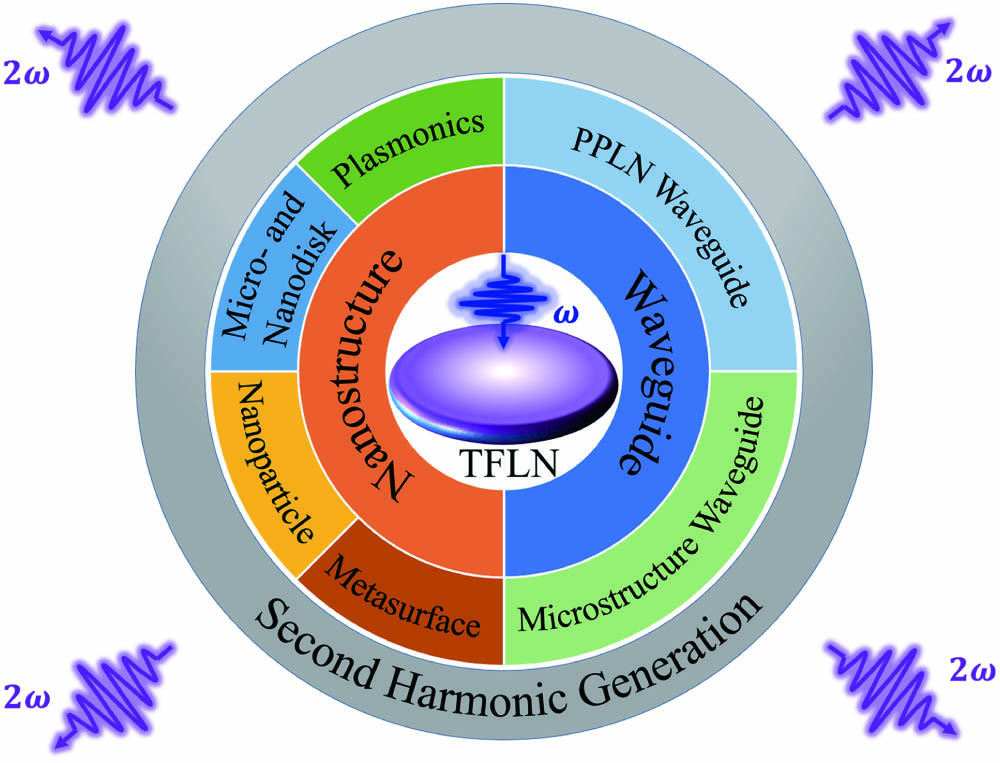
Fig. 1. Summary of different approaches of SHG based on TFLN technology.
Fig. 2. (a) Schematic and false-color SEM image of a periodically poled nanophotonic waveguide
[39]; Copyright 2018, Optical Society of America. (b) SH confocal microscopy of the PPLN thin film fabricated by microelectrode poling and the cross section of the LNOI ridge waveguide
[40]; Copyright 2020, AIP Publishing. (c) Schematic of the cascading EO coupling and SHG process in the PPLN ridge waveguide
[41]; Copyright 2019, Optical Society of America. (d) Schematic illustration of the PPLN waveguide with poling electrodes
[42]; Copyright 2019, Optical Society of America.
Fig. 3. (a) Demonstration of efficient SHG in PPLN microring resonators
[46]; Copyright 2019, Optical Society of America. (b) Schematic of the periodically grooved structure of an LN waveguide and cross-section image of the
X-cut LNOI waveguide
[44]; Copyright 2017, Optical Society of America. (c) Schematic and working principle of the metasurface-assisted LN nanophotonic waveguide
[47]; Copyright 2017, Springer Nature. (d) Schematic of a rib-loaded GA-QPM waveguide with a sinusoidal modulation of the width along with the optical mode profiles of the fundamental and SH TE modes at a grating width of 1095 nm
[45]; Copyright 2017, AIP Publishing.
Fig. 4. (a) Schematic of the LN powder to form the cavity behavior in the SH emission at a certain pump intensity
[50]; Copyright 2019, American Physical Society. (b) SEM images of single LN nanocubes to obtain the maximal SHG
[51]; Copyright 2019, American Chemical Society.
Fig. 5. (a) Images of SHG in an LN metasurface and SHG power depending on average power of the fundamental harmonic (FH) beam
[52]; Copyright 2020, American Chemical Society. (b) Schematic of LN nonlinear metasurfaces fabricated on an
X-cut LN film residing on a fused quartz substrate. Left inset gives a typical SEM image of the cross section of the metasurface, and the right inset presents the measured second-order susceptibility of the LN film used in this study
[53]; Copyright 2021, John Wiley and Sons.
Fig. 6. (a) SEM images showing the mask for ion-beam-enhanced etching (IBEE) (Cr/SiO
2 pillars) and measured SH enhancement factor and linear reflection spectrum of the fabricated sample
[59]; Copyright 2015, American Chemical Society. (b) Schematic of the experiment mounted using index matching oil in a typical Kretschmann geometry
[70]; Copyright 2018, Optical Society of America.
Fig. 7. (a) Scanning-electron micrograph of LN microresonators to achieve modal dispersion
[75]; Copyright 2017, Optical Society of America. (b) SEM images of the LN microdisk PM
[77]; Copyright 2020, IOP Publishing. (c) SEM image of the
X-cut LN microdisk and spectra of the pump light, the second-harmonic wave, and the third-harmonic wave. SHG conversion efficiency as a function of the in-coupled power
[78]; Copyright 2019, American Physical Society. (d) Schematic depiction of the proposed nanostructure for generating SH and nonlinear simulations
[82]; Copyright 2020, De Gruyter.
| Year | TFLN Structure | Poled/Coupling Region Length L (mm) | FF Power () | Coupling Loss (dB/facet) | Waveguide Propagation Loss (dB/cm) | () | Institute |
|---|
| 2011 | Plasmonic waveguide[60] | 1 | 1 W (1550 nm) | – | – | 1.3% | Nanjing University | | 2015 | Nanoscale LN waveguides[61] | 0.9 | 737 µW (1411 nm) | – | 61 | 6.9 | Friedrich Schiller Universität Jena | | 2017 | PE channel waveguide[36] | 3.2 | 1 mW (1385 nm) | – | 2.5 | 48 | Shandong University | | 2016 | Rib-loaded SiN-PPLN[22] | 4.8 | 0.5 mW (1530 nm) | ∼6.8 | | 160 | University of California | | 2017 | Metasurface-assisted PM LN waveguide[47] | 0.019 | 109 V/m/20 mW (1640 nm) | – | – | 1660 | Harvard University | | 2017 | GA-QPM LN ridge waveguide[45] | 4.9 | 84 mW (1568 nm) | 6.5 | 1 | 0.8 | University of Central Florida | | 2017 | Integrated TFLN waveguide[44] | 3 | 18.3 µW (1550 nm) | 4.8 | | 41 | Harvard University | | 2016 | Diced ridge PPLN waveguides[62] | 5.8 | 6.6 mW (1550 nm) | – | 0.57 | 77.9 | Shandong University | | 2018 | PPLN on silicon[63] | 20 | 10 mW (1547 nm) | – | 0.2 | 1230 | University of Central Florida | | 2018 | Nanostructured PPLN waveguide[39] | 4 | 220 mW (1550 nm) | ∼10 | – | 2600 | Harvard University | | 2018 | LN nanophotonic waveguide[64] | 8 | ∼1 mW (1540 nm) | 5 | 0.54 | 22.2 | University of Rochester | | 2019 | PPLN microrings[46] | – | 115 µW (1617 nm) | – | – | 250,000%/W | Yale University | | 2019 | PPLNOI ridge waveguide[41] | 10 | 10 mW (1590 nm) | – | – | 0.04 | Shanghai Jiao Tong University | | 2019 | Dry-etched[65] | 0.6 | 1 mW (1540 nm) | 6 | 3 | 4600 | University of Central Florida | | 2019 | Dry-etched[21] | 4 | 2.95 mW (1550 nm) | 4.3 | 0.3 | 2200 | Stevens Institute of Technology | | 2020 | Z-cut PPLNOI waveguide[66] | 1 | –(1550 nm) | | | 2400 | Stevens Institute of Technology | | 2020 | Dry-etched PPLN[67] | 5 | 0.1 mW (1570 nm) | | | 2000 | University of California | | 2020 | PPLNOI ridge waveguide[40] | 6 | 397 µW (1470 nm) | – | – | 3061 | Nanjing University+Sun Yat-sen University | | 2020 | Birefringent phase-matching LN waveguide[68] | 10 | 4500 W (1064 nm) | – | 0.58 | 0.87% | Shandong University | | 2020 | Shallow-etched TFLN waveguides[42] | 5 | 10 mW (1560 nm) | 7.7 | 1 | 3757 | University of California | | 2020 | PPLN waveguide[69] | 6 | 60 fJ (2050 nm) | – | | 1000 | Stanford University | | 2020 | LN slab waveguides by grating metasurfaces[48] | 0.05 | 25 mW (1064 nm) | – | – | | Nanjing University |
|
Table 1. Comparisons of SHG Conversion Efficiency of Different TF-PPLN Waveguides
| Year | Structure | Mechanism | Structure Parameter (Radius R, Diameter D, Height H, Thickness T) | Peak Pump Intensity/Power () | Q Factor () | | ()/Unstructured LN | Institute |
|---|
| 2012–2013 | Embedded Ag-LN[83,84] | Fabry–Perot resonance | Coaxial aperture (Rinner, Router, H = 120 nm) | –1550 nm | – | – | | FEMTO-ST, CNRS | | 2014 | LN microdisk resonators[85] | Cavity resonance | LN microdisk (D = 28 µm, T = ∼300 nm) | 1.8 mW (1546 nm) | (1507 nm) | – | 0.109 | Harvard University | | 2015 | High-Q LN microresonator[76] | Femtosecond laser micromachining | LN microdisk (D = ∼82 µm, T = ∼670 nm) | 54.6 µW (1550 nm) | (1550 nm) | – | | Shanghai Institute of Optics and Fine Mechanics | | 2015 | LN-filled gold nanorings[59] | Plasmonic resonance | Ring Rinner, Router, H = 100 nm) | (820 nm) | – | – | | Friedrich Schiller University Jena | | 2017 | LN microdisk resonator[75] | Broadband SPDC | LN microdisk (R = 45 µm, T = 300 nm) | 115 µW (1549.32 nm) | (1549.32 nm) | – | | University of Rochester | | 2018 | PPLN microcavity[74] | Whispering gallery mode (WGM) | PPLN microdisk (D = ∼80 µm, T = 700 nm) | 1.1 mW (1550 nm) | | – | | Nankai University | | 2018 | Gold deposited on TFLN[70] | Plasmonic SHG | Gold film (T = ∼30 nm) | (1240 nm) | – | | – | Macquarie University | | 2018 | LN nanodisks on an Al substrate[81] | Anapole resonances | LN nanodisk (D = 256 nm, H = 70 nm) | (351.3 nm) | – | | – | Institute of Lasers, State Academy of Sciences | | 2019 | On-chip monocrystalline TFLN microdisk resonator[78] | QPM | LN microdisk (D = ∼30 µm, T = 600 nm) | 0.25 mW (1547.8 nm) | (1547.8 nm) | – | 9.9%/mW | Shanghai Institute of Optics and Fine Mechanics | | 2019 | LNO nanocubes[51] | Mie resonances | Nanocube (200 nm) | (720 nm) | – | – | | ETH Zürich | | 2019 | Periodic LN bar and LN disk[24] | Fano resonances | Bar and disk (D = 700 nm, T = 340 nm, L = 1100 nm) | (1605 nm) | 2350 (1605 nm) | | – | Jinan University | | 2019 | Superfine LN powder[50] | Cavity-enhanced SHG | – | (793.5 nm) | – | – | – | Shanghai Jiao Tong University | | 2020 | BPPLN microcavities[49] | Multiple reciprocal vectors | Minimum domain unit (width = 100 nm) | 0.02 mW (1550 nm) | | – | | Nankai University | | 2020 | LNOI wafer[86] | Fabry–Perot resonance | LN film (H = 196.8 nm) | (840 nm) | – | | – | Nankai University | | 2020 | Nanostructured LN[82] | Anapole resonances | LN nanodisk (D = 432 nm, H = 104 nm) | (565.4 nm) | – | | 0.1711 | Jinan University | | 2020 | LN metasurface[52] | ED and MD Mie resonances | Nanocube (period = 870 nm, length = 700 nm) | (1550 nm) | – | | | Friedrich Schiller University Jena | | 2021 | LN nanograting metasurfaces[83] | Mie resonance | Metasurface (period D = 600 nm, H = 235 nm) | (820 nm) | – | | | Nankai University | | 2021 | Integrated LN microresonators[87] | Ultrahigh Q performance | LN microdisk (D = 1030 µm) | 5 µW (1550 nm) | () | – | 602%/mW | Shanghai Institute of Optics and Fine Mechanics |
|
Table 2. Performance Comparisons of Different Micro- and Nanostructures Based on TFLN

![(a) Schematic and false-color SEM image of a periodically poled nanophotonic waveguide[39]; Copyright 2018, Optical Society of America. (b) SH confocal microscopy of the PPLN thin film fabricated by microelectrode poling and the cross section of the LNOI ridge waveguide[40]; Copyright 2020, AIP Publishing. (c) Schematic of the cascading EO coupling and SHG process in the PPLN ridge waveguide[41]; Copyright 2019, Optical Society of America. (d) Schematic illustration of the PPLN waveguide with poling electrodes[42]; Copyright 2019, Optical Society of America.](/richHtml/col/2021/19/6/060012/img_002.jpg)
