Abstract
We report on the effect of inserted photonic crystalline (Ph-C) in the GaN epitaxial layer on the incorporation of the indium component for the InGaN-based green LED. The adoption of Ph-C in the GaN layer shifted the Raman peak value of E2 mode of GaN to lower frequency and resulted in a tensive stress relief. The stress relief can be attributed to strained lattices restoring in the matrix of Ph-C and the GaN pseudo-epitaxy over the air-void of the Ph-C. Moreover, the HRXRD rocking curves and AFM results show that the insertion of Ph-C also improves the crystal quality. With the inserted Ph-C, the indium component in the multiple quantum wells of the green LED (Ph-C LED) was enhanced. This resulted in a 6-nm red-shift of the peak wavelength. Furthermore, the LOP of the Ph-C LED was enhanced by 10.65% under an injection current of 20 mA.We report on the effect of inserted photonic crystalline (Ph-C) in the GaN epitaxial layer on the incorporation of the indium component for the InGaN-based green LED. The adoption of Ph-C in the GaN layer shifted the Raman peak value of E2 mode of GaN to lower frequency and resulted in a tensive stress relief. The stress relief can be attributed to strained lattices restoring in the matrix of Ph-C and the GaN pseudo-epitaxy over the air-void of the Ph-C. Moreover, the HRXRD rocking curves and AFM results show that the insertion of Ph-C also improves the crystal quality. With the inserted Ph-C, the indium component in the multiple quantum wells of the green LED (Ph-C LED) was enhanced. This resulted in a 6-nm red-shift of the peak wavelength. Furthermore, the LOP of the Ph-C LED was enhanced by 10.65% under an injection current of 20 mA.Introduction
Nitride-based materials have been reported to be a promising semiconductor for high brightness light-emitting diodes (LED), and high power and high frequency device, due to their direct and wide bandgap (0.6–6.2 eV)[1]. InGaN-based multiple quantum well (MQW) green LEDs have been widely used in full color display, landscape lighting, and traffic light due to their merits of high efficiency, long life time and small size. Although great progress has been achieved in the fabrication of green LEDs, enhancing the incorporation of indium component for the In-rich InGaN/GaN MQW was one of the bottlenecks for making long-wavelength and high-performance green LEDs. One of the obstacles to incorporation of In components is the mismatch stress in the epitaxial layer, which originates from both the lattice mismatching and thermal expansion coefficients difference in the c-plane between GaN and sapphire substrate[2, 3]. The dominant strain in the GaN grown on the c-plane sapphire origins from the thermal coefficient incompatibility (62%), and lattice constant difference (13%)[1]. In order to grow a thicker GaN layer on a sapphire substrate, compressive stress was generated during the cooling down process mainly because of the difference of the thermal expansion coefficients. In the GaN epilayer grown on a 2-inch sapphire substrate, the compressive stress and wafer bending can reach ~200 MPa and ~60 μm[4], which is not satisfactory for the massive production. The stress, due to the hetero-epitaxy of GaN on a foreign substrate, has a great effect on the incorporation of the indium component for the In-rich InGaN-based green LED [5].
Many methods have been proposed and employed to relax the stress in the GaN epilayer grown on sapphire substrate, such as by using AlGaN/AlN transition layer[6], low-temperature AlN layer[7], AlN/GaN superlattice (SLS)[8, 9], patterned sapphire substrate[10, 11], laser treatment[4], nanopillars[12], carbon nanotubes[13], V-grooves[14], step-graded InxGa1–xN/GaN layer[15], high-energy electron irradiation[16], dislocation glide[17], pre-strained interlayer[18], indium surfactant[19] and etc. This paper aimed to investigate a new stress relief method by inserting Ph-C into the GaN epilayer grown on sapphire to improve the incorporation of indium component for InGaN-based green LEDs.
Experiment
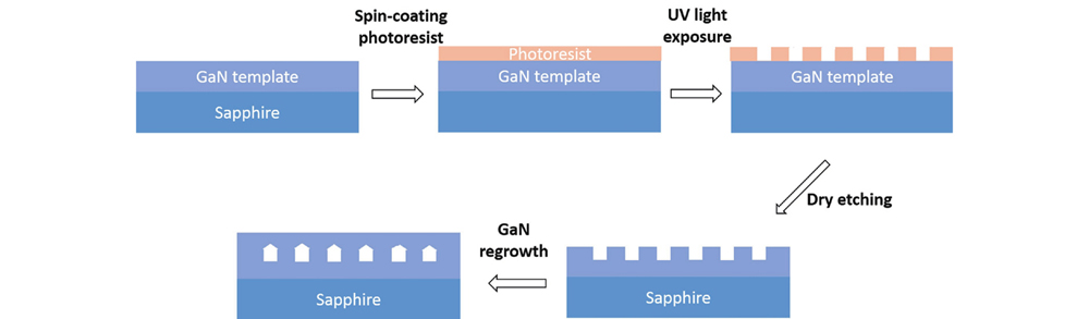
A control sample and a GaN sample introducing Ph-C (Ph-C sample) were grown on c-plane sapphire substrates in a Veeco metal-organic chemical vapor deposition system. First, two GaN/sapphire templates were grown: The sapphire substrates were cleaned at 1015 °C in H2 atmosphere, followed by the growth of GaN buffer layer at temperature of 560 °C (about 30 nm thick); Subsequently, a 2 μm undoped GaN was grown at a temperature of 1150 °C. Then, a 1 μm thick un-doped GaN epilayer was grown directly on the GaN template for the control sample. For the Ph-C sample, the fabrication process started with the spinning of 600 nm thick photoresist on the GaN/sapphire template, followed by the transfer of monolayer of polystyrene sphere on the surface of the photoresist; Subsequently, the UV-exposure was conducted and followed by the inductively coupled plasma (ICP) etching, forming nano-voids with a diameter of about 200 nm and a depth of 400 nm. Then, cleaning of the etched wafer and regrowth of GaN on the Ph-C were conducted with the same growth condition as the control sample. The InGaN-based green LED epitaxial structure was then grown on the two templates. At first, a 200 nm n-GaN layer was grown on the n-GaN/sapphire substrate at 900 °C. Then, an InGaN/GaN MQWs sample consisting of eight pairs of 3.5 nm undoped InGaN wells and 15 nm Si doped GaN barriers was grown. Mg-doped p-AlGaN EBL with a uniform aluminum content of 20% was grown directly on the MQWs. The thickness of the p-AlGaN EBL was 30 nm for both samples. On top of the EBL, a 120-nm thick p-type GaN was grown. Detailed information about the experiment process can be found in the early works of our team[20-22].
Results and discussion
A schematic diagram of the fabrication process flow to realize Ph-C sample is shown in Fig. 1. The GaN grown on Ph-C completely coalesces in the lateral direction, with a thickness of 0.1 μm in the vertical direction, which is measured by the cross-sectional scanning electron microscope (SEM) shown in the Fig. 2. As depicted in Figs. 3(a) and 3(b), atomic force microscope (AFM) measurement shows that the root-mean-square (RMS) roughness of the Ph-C sample surface is about 0.194 nm (Fig. 3(b)), while that of the control sample is 0.317 nm (Fig. 3(a)), indicating an improvement of the surface roughness. Figs. 3(c) and 3(d) showed the AFM images of both control sample and Ph-C sample after KOH etching. The Ph-C sample owns a lower density of etched pits after KOH etching, in comparation with the control sample. The pit density, which is often considered equal to the density of threading dislocations[23], is estimated to be 7.1 × 10⁹ and 3.3 × 109 cm−2 for the control sample and Ph-C sample, respectively. These results suggest that the inserting of Ph-C can effectively improve the surface quality, through the bending of the threading dislocation and the reduction of the dislocation penetration to the surface.

Figure 1.(Color online) Schematic of the fabrication process flow to realize Ph-C sample.
Figure 2.The cross-sectional scanning electron microscope of the Ph-C sample.
Figure 3.(Color online) Atomic force microscopes surface topography of (a) control sample, (b) Ph-C sample, (c) control sample after KOH etching, (d) Ph-C sample after KOH etching.
Raman measurements performed with a laser of excitation wavelength of 514 nm at room temperature is present in the Fig. 4. It is well known that GaN epilayer grown on non-native substrates, has stress-change-related lattice vibration, originating from the thermal coefficient difference and lattice mismatching between sapphire and GaN layer. Therefore, the peak value of the E2 (high) mode shifts to a higher (lower) value when the GaN layer is under compressive (tensive) stress. The strain in GaN layer can be estimated by the shift value of the E2 mode[24]. It can be seen in Fig. 4, the peak values of E2 mode of the two samples are smaller than that of the stress-free GaN, indicating both of the samples are under tensive stress states. Compared with the peak value (560.1 cm–1) of control sample, that of Ph-C sample shifts to higher value (561.3 cm–1), indicating reduction of tensive stress in the GaN layer. The relation between stress in the GaN layer and the E2 mode of peak value shift is given by
, where the
is the difference between the measured E2 value and that of the stress-free GaN layer (567.6 cm–1) and
is the stress in the C-plane, respectively[2, 25]. Compared with the E2 mode of the stress-free GaN, the E2 mode peak shifts are 6.3 and 7.5 cm–1 for Ph-C sample and control sample, respectively. As a result, the tensive stress was reduced from 2.93 to 2.46 GPa for the Ph-C sample. It is quite clear that a tensive stress relief of 0.47 GPa is realized by inserting the Ph-C into the GaN layer.
Figure 4.(Color online) Raman spectra of control sample and Ph-C sample measured at room temperature.
Two reasons may contribute to the strain relief for the Ph-C sample: (1) The strain in the GaN Ph-C was partially relaxed in the ICP process. The stress was relieved in three mechanisms in the ICP process[26]: 1) The sidewall of the tensive matrix (the un-etched region in the Ph-C) moves outwards due to the asymmetric strain at the free surface of the edge, with the underneath GaN layer distorted, partially decreasing the deformation of the crystal lattices in the matrix and then relaxing the strain. 2) The sidewall of the matrix moves outwards, keeping the underneath GaN layer un-distorted. 3) The sidewall of the matrix and the underneath GaN layer under the sidewall bend down, accompanied by the central portion bulging upwards. The combination of these effects results in the GaN matrix curving upwards. Therefore, the highest in-plane tensive stress appears at the bottom of the matrix, decreasing along the c-axis and being in a relaxation state at the matrix surface. Furthermore, the stress in the matrix surface decreases lateral toward the matrix sidewall in the c-plane. As a result, the strain relief in the matrix reduces the lattice deformation in the GaN subsequently grown on the matrix and then its stress. (2) The GaN wings by lateral growth have smaller stress due to its hanging over the air-void. After the regrowth of the GaN epilayer with the nanoscale lateral epitaxial technique on the Ph-C, most parts of the wings, except the coalescence boundaries, are under unstrained states in the c-plane, due to their hanging freely above the air-void of the Ph-C, which means a reduced average strain value in the upper GaN epitaxy layer.
Fig. 5(a) shows the HRXRD 2θ–ω patterns of the two LED samples. Generally, the position difference between the 0th satellite peak and the GaN peak was related to the average In composition across the active region[27]. The larger the position difference, the more the In incorporation. It can be seen that the 0th satellite peak of the Ph-C shift leftward compared with the controlled sample, which indicated that In incorporation was enhanced.
Figure 5.(Color online) (a) HRXRD 2θ–ω patterns of the two LED samples. (b) HRXRD (002) rocking curves of the Ph-C sample and the control samples. (c) HRXRD (102) rocking curves of the Ph-C sample and the control samples.
Beside the stress relief, the inserted Ph-C also have an influence on the crystal quality. The AFM results show that the pits were reduced at the surface of the Ph-C sample, which means a reduction of the threading dislocations. To further prove the improvement of the crystal quality, HRXRD rocking curves measurement of GaN for symmetric (002) and asymmetric (102) planes were conducted to confirm the reduction of the dislocations, which is shown in Figs. 5(b) and 5(c). It can be seen that the full width at half maximum (FWHM) of the (002) and (102) plane for control sample are 130.6 and 369.8 arcsec, respectively, while that of Ph-C sample are 120.4 and 321.2 arcsec, respectively. It is well known that the FWHM of the GaN (102) plane is ascribed to the existence of threading dislocation in the epilayer, which means that the observed reduction in the FWHM of the (102) plane of Ph-C sample is attributed to the reduction of threading dislocations[28]. The reduction of the threading dislocations in the Ph-C sample can be attributed to two reasons: (1) the air-voids of the Ph-C stopped the threading dislocations, originating from the GaN template, from propagating into the upper layers; (2) the lateral coalescence of GaN grown on the Ph-C results in a bending of dislocations stemming from the matrix surface, which is a common phenomenon in epitaxial lateral overgrowth. These results are consistent with the AFM findings that the GaN crystal quality is significantly improved by inserting Ph-C into the GaN layer.
Fig. 6(a) shows the room temperature PL spectra of the Ph-C LED and the compared LED. The PL peak position of Ph-C LED and the compared LED is 525.9 and 519.9 nm, respectively, thereby with a peak wavelength red-shift of 6 nm for Ph-C LED. The luminescence energy change can be attributed to the strain-related compositional variation. The LOP and EQE as a function of forward current density for Ph-C LED and the compared LED is shown in the Fig. 6(b). At the forward current of 20 mA, a 5% increasing in the output power is achieved by inserting a Ph-C structure. The Ph-C LED shows a 10.65% enhancement of the EQE under the injection current of 20 mA. The improvement of the EQE suggests that the inserted Ph-C layer prevented the dislocation defect from penetrating upward into the multi-quantum-well region. In addition, the inserted photonic crystal in the n-GaN also improves the diffuse reflection of photons in the substrate direction, which improves the light extraction efficiency of LED, then enhancing the external quantum efficiency of LED.
Figure 6.(Color online) (a) PL spectra of compared LED and Ph-C LED measured at room temperature. (b) EQE of compared LED and Ph-C LED measured under different injection currents. (c) LOP of compared LED and Ph-C LED measured under different injection currents.
Conclusion
In conclusion, we investigated the effect of the inserted Ph-C in the GaN epitaxial layer on the incorporation of indium component for the InGaN-based green LED. The Raman results show that the E2 mode value shifts to the higher value in the Ph-C sample, indicating that the tensive stress was relaxed in the Ph-C sample. HRXRD results showed that the insertion of the Ph-C also reduced the dislocation density which was consistent with the AFM results. The HRXRD results also reveals that the In incorporation in the active region was enhanced for the Ph-C LED, resulting in a 6 nm red-shift of the PL peak wavelength. Moreover, the LOP of the Ph-C LED was enhanced by 10.65% under the injection current of 20 mA.
References
[1] S Strite. GaN, AlN, and InN: A review. J Vac Sci Technol B, 10, 1237(1992).
[2] C Kisielowski, J Krüger, S Ruvimov et al. Strain-related phenomena in GaN thin films. Phys Rev B, 54, 17745(1996).
[3] T Kozawa, T Kachi, H Kano et al. Thermal stress in GaN epitaxial layers grown on sapphire substrates. J Appl Phys, 77, 4389(1995).
[4] C H Chen, M H Liao, L C Chang et al. Relaxation of residual stress in bent GaN film on sapphire substrate by laser treatment with an optimized surface structure design. IEEE Trans Electron Devices, 60, 767(2013).
[5] J Napierala, D Martin, N Grandjean et al. Stress control in GaN/sapphire templates for the fabrication of crack-free thick layers. J Cryst Growth, 289, 445(2006).
[6] H Ishikawa, G Y Zhao, N Nakada et al. GaN on Si substrate with AlGaN/AlN intermediate layer. Jpn J Appl Phys, 38, L492(1999).
[7] A Dadgar, J Bläsing, A Diez et al. Metalorganic chemical vapor phase epitaxy of crack-free GaN on Si (111) exceeding 1 µm in thickness. Jpn J Appl Phys, 39, L1183(2000).
[8] E Feltin, B Beaumont, M Laügt et al. Stress control in GaN grown on silicon (111) by metalorganic vapor phase epitaxy. Appl Phys Lett, 79, 3230(2001).
[9] P K Kandaswamy, C Bougerol, D Jalabert et al. Strain relaxation in short-period polar GaN/AlN superlattices. J Appl Phys, 106, 013526(2009).
[10] M T Wang, K Y Liao, Y L Li. Growth mechanism and strain variation of GaN material grown on patterned sapphire substrates with various pattern designs. IEEE Photonics Technol Lett, 23, 962(2011).
[11] J H Lee, J T Oh, Y C Kim et al. Stress reduction and enhanced extraction efficiency of GaN-based LED grown on cone-shape-patterned sapphire. IEEE Photonics Technol Lett, 20, 1563(2008).
[12] W J Tseng, M Gonzalez, L Dillemans et al. Strain relaxation in GaN nanopillars. Appl Phys Lett, 101, 253102(2012).
[13] A H Park, T H Seo, S Chandramohan et al. Efficient stress-relaxation in InGaN/GaN light-emitting diodes using carbon nanotubes. Nanoscale, 7, 15099(2015).
[14] K Cheng, M Leys, S Degroote et al. Formation of V-grooves on the (Al, Ga)N surface as means of tensile stress relaxation. J Cryst Growth, 353, 88(2012).
[15] M A Hossain, M R Islam. A theoretical calculation of misfit dislocation and strain relaxation in step-graded InxGa1–xN/GaN layers. Adv Mater Res, 403–408, 456(2011).
[16] X T Fu, T D Ma, S M Wang et al. Strain relaxation of GaN heterostructure induced by high-energy electron irradiation. Chin J Rare Met, 36, 450(2012).
[17] E C Young, J S Speck. Heteroepitaxial lattice mismatch stress relaxation in nonpolar and semipolar GaN by dislocation glide. ECS Trans, 50, 797(2013).
[18] L Liu, L Wang, D Li et al. Influence of indium composition in the prestrained InGaN interlayer on the strain relaxation of InGaN/ GaN multiple quantum wells in laser diode structures. J Appl Phys, 109, 073106(2011).
[19] D Won, X J Weng, J M Redwing. Effect of indium surfactant on stress relaxation by V-defect formation in GaN epilayers grown by metalorganic chemical vapor deposition. J Appl Phys, 108, 093511(2010).
[20] N Zhang, Z Liu, T B Wei et al. Effect of the graded electron blocking layer on the emission properties of GaN-based green light-emitting diodes. Appl Phys Lett, 100, 053504(2012).
[21] C X Du, T B Wei, H Y Zheng et al. Size-controllable nanopyramids photonic crystal selectively grown on p-GaN for enhanced light-extraction of light-emitting diodes. Opt Express, 21, 25373(2013).
[22] N Zhang, Z Liu, Z Si et al. Reduction of efficiency droop and modification of polarization fields of InGaN-based green light-emitting diodes via Mg-doping in the barriers. Chin Phys Lett, 30, 087101(2013).
[23] A Minj, D Cavalcoli, A Cavallini et al. Strain distribution and defect analysis in III-nitrides by dynamical AFM analysis. Nanotechnology, 24, 145701(2013).
[24] V Y Davydov, Y E Kitaev, I N Goncharuk et al. Phonon dispersion and Raman scattering in hexagonal GaN and AlN. Phys Rev B, 58, 12899(1998).
[25] J M Wagner, F Bechstedt. Phonon deformation potentials of α-GaN and-AlN: An ab initio calculation. Appl Phys Lett, 77, 346(2000).
[26] S C Jain, M Willander, H Maes. Stresses and strains in epilayers, stripes and quantum structures of III-V compound semiconductors. Semicond Sci Technol, 11, 641(1996).
[27] F M Morales, D González, J G Lozano et al. Determination of the composition of InxGa1−xN from strain measurements. Acta Mater, 57, 5681(2009).
[28] M A Moram, M E Vickers. X-ray diffraction of III-nitrides. Rep Prog Phys, 72, 036502(2009).