Abstract
Recently, fundamental properties and practical applications of two-dimensional (2D) materials have attracted tremendous interest. Micro/nanostructures and functional devices in 2D materials have been fabricated by various methods. Ultrafast direct laser writing (DLW) with the advantages of rich light-matter interactions; unique three-dimensional processing capability; arbitrary-shape design flexibility; and minimized thermal effect, which enables high fabrication accuracy resolution, has been widely applied in the fabrication of 2D materials for multifunctional devices. This timely review summarizes the laser interactions with 2D materials and the advances in diverse functional photonics devices by DLW. The perspectives and challenges in designing and improving laser-fabricated 2D material photonic devices are also discussed.Two-dimensional (2D) materials usually refer to materials consisting of mono or a few layers of atoms, with thicknesses varying from one atomic layer to more than 10 nm[1–7]. Various 2D materials have been successfully isolated, including graphene, hexagonal boron nitride (h-BN), transition metal dichalcogenides (TMDCs), black phosphorus (BP), and perovskite[2,8–17]. 2D materials exhibit exotic physical and chemical properties such as atomic thickness, strong nonlinear optical properties, magnetic properties, and excellent mechanical strength that are different from their bulk counterparts, opening new opportunities for nanodevices, especially photonics applications[18].
Functional micro/nanoscale 2D materials devices have been proposed and fabricated using various fabrication techniques in order to fulfil the intriguing properties of the 2D materials[19–23]. Ultrafast direct laser writing (DLW) has been established as a nanometer patterning enabler because of its unique multidimensional processing capability, arbitrary-shape design flexibility, minimum thermal impact enabling high fabrication resolution of tens of nanometers, and rich light-matter interaction mechanisms and dynamics[24–27]. Currently, this flexible fabrication method has been widely used in 2D materials patterning, modification, and functionalization, demonstrating versatile capabilities. Some conceptual device designs have been proposed and demonstrated using DLW[28–35].
This timely review captures these exciting advancements and provides an in-depth summary and understanding of the latest functional photonic devices enabled by 2D materials and the DLW method. First, we briefly overview the physical property changes of 2D materials upon laser exposure. Then, we analyze the advantages and limitations of 2D materials functional photonic devices fabricated by DLW toward practical applications. Finally, we discuss the challenges, opportunities, and perspectives in this field.
Sign up for Chinese Optics Letters TOC. Get the latest issue of Chinese Optics Letters delivered right to you!Sign up now
Based on laser conditions and material responses, laser-matter interactions may involve several processes and the process is sometimes complicated: single/multi-photon absorption, material ablation under laser exposure, phase change and agglomeration of nanostructures, and chemical/physical properties modifications[36–38]. These processes lead to different physical and chemical property changes of materials, like tuning refractive indices () and extinction coefficients (), bandgap engineering, conductivity changes, and surface wetting properties (hydrophilic or hydrophobic)[16,35] which are the fundamental basis for various functional device designs, like photonics devices or optoelectronics elements. The light and 2D materials interactions can enable micro/nano-patterning with a high resolution of tens of nanometers[39], 2D materials monolayer laser thinning in order to obtain the thinnest materials[40], and laser doping of various 2D materials to obtain functionalized materials for practical applications[41], which are critical for high-resolution processing and functionalization of 2D materials down to a monolayer accuracy[32,42].
The physical and chemical changes of 2D materials induced by laser illumination provide the fundamental mechanisms for designing various optical devices. For example, the n and k values can be changed during the DLW process[43,44], which is beneficial for phase modulation in flat optics, including the lens and grating[43,45,46]. The bandgap of 2D materials can be effectively modulated by laser irradiation, leading to the formation of luminescent or other functional semiconducting devices[47]. The integration of highly nonlinear 2D materials with all-optical communication chips can add extra functionalities without increasing the footprint of the devices[45,48–52]. These exciting experimental advancements showed an unprecedented potential of 2D materials shaping the integrated photonic field, offering enormous new opportunities. In the following, some recent interesting demonstrations of functional photonic devices with 2D materials by ultrafast direct laser processing are highlighted.
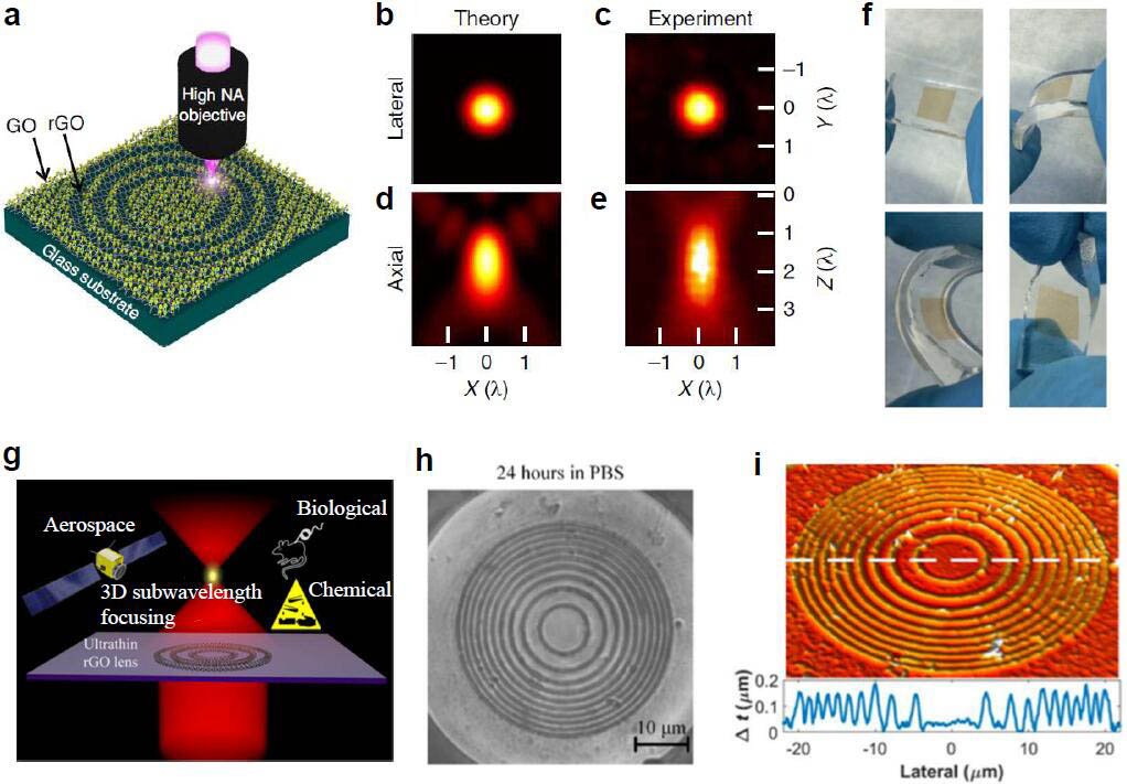
In the past two decades, tremendous efforts have been devoted to designing ultrathin flat lenses[53], such as micro Fresnel lenses[54], plasmonic lenses[55], and metasurface lenses[56], toward highly integrated photonic circuitry. But it is challenging to realize ultrathin lenses with subwavelength focusing resolution, broadband wavelength operation, and facile manufacturing because light needs to be modulated sufficiently to produce the desired phase or amplitude by passing through a natural medium with a thickness much larger than the wavelength of light. Zheng et al. designed an ultrathin (200 nm in thickness) flat graphene oxide (GO) lens based on the giant and changes upon ultrafast laser exposure, which led to the significant phase and amplitude manipulations of an incident light beam[43].
Figures 1(a)–1(e) show a GO flat lens, which is composed of several submicrometer concentric rings of GO and reduced graphene oxide (rGO). Ideally, the lens design relying on the constructive and destructive interferences within the focal region requires the phase difference between adjacent rGO and GO zones to be equal to π for a high focusing efficiency. Although the phase difference is smaller than π, the amplitude modulation that resulted from the concomitant augments in extinction coefficients is responsibe for enhancing the focusing efficiency over a broad bandwidth. To illustrate its mechanical flexibility and the versatility in wavefront manipulations, a large-scale GO thin film is integrated on a flexible polydimethylsiloxane substrate, as shown in Fig. 1(f). The excellent mechanical robustness of GO films maintains the optical performance after bending and stretching, making it a promising candidate for flexible imaging devices.
![(a) Conceptual design and laser fabrication of the GO ultrathin lens. (b), (d) Theoretical focal intensity distributions in the lateral and axial directions. (c), (e) Experimental focal intensity distributions along the lateral and axial directions. (f) Bending and twisting of the GO thin film on a polydimethylsiloxane substrate. (a)–(f) Reproduced with permission[43]. Copyright 2015, Nature Publishing Group. (g) Graphene ultrathin flat lens working in harsh environment. rGO lens after the PBS test. (h) Microscopic image of the rGO lens after immersing in PBS for 24 h. (i) Topological profile of the rGO lens after PBS test. (g)–(i) Reproduced with permission[57]. Copyright 2018, American Chemical Society.](/Images/icon/loading.gif)
Figure 1.(a) Conceptual design and laser fabrication of the GO ultrathin lens. (b), (d) Theoretical focal intensity distributions in the lateral and axial directions. (c), (e) Experimental focal intensity distributions along the lateral and axial directions. (f) Bending and twisting of the GO thin film on a polydimethylsiloxane substrate. (a)–(f) Reproduced with permission[43]. Copyright 2015, Nature Publishing Group. (g) Graphene ultrathin flat lens working in harsh environment. rGO lens after the PBS test. (h) Microscopic image of the rGO lens after immersing in PBS for 24 h. (i) Topological profile of the rGO lens after PBS test. (g)–(i) Reproduced with permission[57]. Copyright 2018, American Chemical Society.
Following this, Cao et al. showed a graphene flat lens can maintain excellent focusing performance in harsh environments for different applications, including a low Earth orbit space, strong corrosive chemicals, and biochemical environment, as shown in Fig. 1(g)[57,58]. To show the stability of the rGO lens in a biological body, the rGO lens was immersed in phosphate-buffered saline (PBS) solution for 24 h at 37°C. The optical microscope image of the rGO lens after the harsh environment treatment is shown in Figs. 1(h) and 1(i), which presents no discernible change and clearly maintains the integrity. In addition, the optical profiler image was taken to confirm that the surface of the rGO lens is not affected by the PBS solution. The graphene lenses have strong environmental stability and can maintain a perfect focusing performance, opening practical application opportunities in biological imaging, space science, high-resolution sensing, and spectroscopy.
In theory, the ultimately thin flat lens is a monolayer of 2D materials. However, it is difficult to achieve a light focusing function in such a small thickness due to an insufficient phase and amplitude modulation and the challenges in operating in such a delicate material. Lin et al. showed an ultrathin flat monolayered lens (thickness: 7 Å) via the DLW method. The lens structure is composed of four concentric rings [Fig. 2(a)]. The lens structures are patterned using a femtosecond laser selective ablation mechanism. This will produce a large refractive index contrast to allow the strong phase and amplitude modulation. The theoretical and experimental intensity distributions of the focal spot in the plane are shown in Figs. 2(b)–2(d), indicating a full width at half-maximum along the direction as high as 0.6[44]. This is the first demonstration of a high-quality diffraction limited focusing being achieved in the visible wavelength region in a monolayer 2D material. Such a monolayer of TMDC crystals can be transferred to an arbitrary substrate, thus making the lens readily integratable with diverse electronic or photonic devices with high performance.
Figure 2.(a) Optical image of a fabricated monolayered lens. (b) Theoretical focal intensity distributions in the lateral directions. (c) Experimental focal intensity distributions along the lateral directions. (d) Intensity distribution of the theoretical and experimental results along the lateral directions. Reproduced with permission[44]. Copyright 2016, Conference on Lasers and Electro-Optics (CLEO).
The ultrathin nature (3.4 Å) and low optical absorption (2.3%) of monolayer graphene limit its capability in providing strong optical modulation, which is critical for optical devices. Graphene metamaterials comprising alternating monolayer GO and monolayer dielectric layers as artificially structured materials to attain an extremely high optical responses have been developed by Yang et al. using layer by layer assembly[45]. DLW can trigger the properties transition in graphene metamaterial by removing the oxygen-functional groups to decrease the bandgap. The conceptual design of the graphene metamaterial architecture and the dynamic photo tuning process are illustrated in Figs. 3(a)–3(c). The tuning process is controlled by varying the laser power, yielding multiple reduction levels when elevating the laser power [(Fig. 3(e)][45].
Figure 3.(a)–(c) Schematic of the dynamic process for in situ phototunable graphene metamaterials. (d) SEM image of the five-layer GO structure clearly showing the layer-by-layer structure. (e) Optical micrographs of reduction and ablation of graphene metamaterials. Changes in (f) refractive index and (g) extinction coefficient as functions of laser power for graphene metamaterials at broadband wavelengths ranging from 200 to 1600 nm. Reproduced with permission[45]. Copyright 2019, American Chemical Society.
The effective and of the graphene metamaterial before and after laser tuning are measured, as shown in Figs. 3(f) and 3(g). The pristine graphene metamaterial exhibits a moderate of about 2, within the measured wavelength. The value of increases beyond 2.5 at 500 nm and reaches 2.7 at 1600 nm when increasing the laser power to 10 μW. The change is at least one order of magnitude larger than conventional photorefractive materials and is indicative of a large dynamic tuning range, which is useful for phase modulation in photonic devices. Before tuning, the metamaterial exhibits a low over the measured wavelength range. The value changes by 0.25 over a wide wavelength range upon laser exposure, which results in a high contrast in light absorption of the laser-reduced graphene metamaterial, providing a mechanism for achieving efficient amplitude modulation. This innovative graphene metamaterial platform with a laser-induced tunability and patterning provides a new solution for ultrathin and ultra-lightweight, highly integrated, and flexible optical systems, opening new avenues for various multidisciplinary applications.
A perfect absorber should be able to absorb radiation at all angles and polarizations over a broadband wavelength range. Ideally, the thickness of such an absorber should be as thin as possible to facilitate efficient thermal energy transfer or conversion from the absorbers to other media. Such perfect absorbers have wide applications in photothermal energy generation, water desalination, and contaminated water treatment. The current challenge is to achieve an outstanding absorption performance at an ultrathin thickness. Lin et al. showed a , 90 nm thick graphene metamaterial with ∼85% absorptivity of unpolarized, visible, and near-infrared light covering almost the entire solar spectrum (300–2500 nm), as shown in Fig. 4[46]. The metamaterial consists of graphene and dielectric layers formed using the self-assembly method[45]. A one-dimensional grating structure couples the light into waveguide modes to achieve broadband absorption over incident angles up to 60°. The grating structure is fabricated using the ultrafast DLW method, which converts the GO to graphene via laser photoreduction. The broad spectral and angular responses of the absorber are ideal for solar thermal applications. Within 40 s of illumination, the graphene metamaterials can be heated to 160°C under sunlight. This device concept opens a novel approach to applications of strongly absorbing large-area photonic devices based on 2D materials, including solar thermal energy harvesting, solar vapor generation, and photodetectors.
Figure 4.(a) Schematic of graphene-based metamaterial absorber. (b) Photograph of the absorber with an area of 50 mm by 25 mm. (c) Optical microscope image of the grating. (d) SEM image of the central part of the grating. (e) Schematic of the set-up to measure the heating of the sample under sunlight. (f) Thermal image of the fabricated large-area absorber sample. (g) Temperature measurement of the GO metamaterial (red), the graphene-based metamaterial absorber (black), and hierarchical graphene foam (green). Reproduced with permission[46]. Copyright 2019, Nature Publishing Group.
Holography has received attention because of its capability to construct arbitrary wavefronts with phase and amplitude information to reconstruct real images. The tunable phase modulation at the subwavelength scale holds a key to the physical realization of holographic 3D images with high efficiencies and wide angles[59]. The tight spatial confinement and continuously tunable linear dispersion resulting from the controllable reduction by laser intensities opens new avenues for holographic displays based on rGO. Li et al. showed that rGO enabled holograms for wide-angle and full-color 3D images, as shown in Fig. 5[60]. This was achieved through the optical index modulation of athermally reduced GO by femtosecond laser beams, allowing for static 3D holographic images with a wide viewing angle up to 52°. Additionally, the spectrally flat optical index modulation in rGO enables wavelength-multiplexed holograms for full-color images. The large and polarization-insensitive phase modulation over in rGO enables the restoration of vectorial wavefronts of polarization discernible images through the vectorial diffraction of a reconstruction beam. Therefore, the technique can be leveraged to achieve compact and versatile holographic components for controlling light.
Figure 5.(a)–(c) rGO holograms by a single femtosecond pulse for 3D images with wide viewing angles and color images. (d)–(h) Vectorial holographic reconstruction of polarization discernible images. Reproduced with permission[60]. Copyright 2015, Nature Publishing Group.
In recent years, organic-inorganic hybrid materials have become a hot topic toward optoelectronic applications. Metal halide lead perovskites, depending on the chemical interaction between organic and inorganic entities, showed diverse and unmatched properties[61–64].
To promote the application of perovskite into integrated devices, microscale color patterning flexibility is a very critical step. Zhou et al. showed spatially resolved modulation of the fluorescence of nanoplatelets by ultrafast DLW (Fig. 6)[65]. As the perovskite nanoplatelets are specially designed with a gradual bromide−iodide composition along the depth, the replacement of iodide ions by bromide ions can be activated under a controlled laser illumination and fluorescence and is thus modulated from red to green. The nanoplatelets (thickness: 500 nm) mainly exhibit a 690 nm emission from the bottom iodine-rich phase. After halide substitution is induced by the ultrafast DLW, a new fluorescence peak appears in the wavelength range of 540−600 nm. The fluorescent color is spatially modulated from red to green, enabling spatially resolved multicolor emission. Arbitrary patterns can be drawn on a wide range of perovskite nanoplatelets, implying the potential for on-chip applications in multicolor displays, lasers, and light-emitting devices.
Figure 6.(a) Commission Internationale de L’Eclairage (CIE) coordinates corresponding to emissions of the thick NP and the laser-fabricated holes. Fluorescence micrographs of (b) thin nanoplatelets and (c) thick nanoplatelets without patterns. A 405 nm laser is used as excitation. (d) Microscopic image of nanoplatelets with laser patterned characters. (e) Fluorescence micrograph of the patterned nanoplatelets under laser excitation. Reproduced with permission[65]. Copyright 2019, American Chemical Society.
In summary, the aforementioned examples show ultrafast DLW is an indispensable tool to fabricate 2D material functional photonics devices with excellent performance. These include ultrathin flat lenses, perfect absorbers, holographic displays, etc., which demonstrate the high resolution, flexibility, and cost-effectiveness of the ultrafast DLW method. Furthermore, ultrafast DLW has been used to locally change the nonlinear properties (nonlinear absorption coefficient and nonlinear refractive index) of a number of 2D materials, including GO materials[48,66,67], black phosphorus[17,68], dichalcogenides[69,70], perovskite[71,72], and others, which offers a new flexibility in directly converting the conventional photonic devices into highly nonlinear systems by simply integrating a layer of 2D materials, leaping the device performance for ultrafast, all-optical communication devices.
Employing the ultrafast DLW method to achieve micro/nanostructures of 2D materials has attracted a growing attention, which has been studied for broad applications. In this review, we have summarized the fabrication of different 2D materials by ultrafast DLW, along with the advancements in applying these materials toward photonics applications. The ultrafast DLW method is a promising strategy for simple, rapid, and large-scale fabrication of various patterns without masks, complicated processing, and harsh chemicals. Ultrafast lasers can drive a wide range of subtractive processes for the patterning and functionalization of 2D materials with a high resolution and accuracy that can be used for scalable processing and realization of the next-generation high-performance portable, integratable, and flexible devices based on 2D materials.
Further advancements rely on both the parallel writing[73] and super-resolution method[74] to achieve better selectivity, nanometer resolution, and manipulation with a high throughput. Combining the ultrafast DLW technique with the parallel writing and super-resolution methods, is promising for developing a novel laser fabrication platform enabling multifunctional and scalable 2D material integrated devices for multidisciplinary research and applications. With the joint efforts from material science, laser physics, and device processing and engineering, we are in a better position than ever to derive innovative solutions to tackle these grand challenges.
References
[1] H. Zhang. ACS Nano, 9, 9451(2015).
[2] J. S. Ponraj, Z.-Q. Xu, S. C. Dhanabalan, H. Mu, Y. Wang, J. Yuan, P. Li, T. S. Thakur, M. Ashrafi, K. Mccoubrey, Y. Zhang, S. Li, H. Zhang, Q. Bao. Nanotechnology, 27, 462001(2016).
[3] F. Xia, H. Wang, D. Xiao, M. Dubey, A. Ramasubramaniam. Nat. Photon., 8, 899(2014).
[4] V. W. Brar, A. R. Koltonow, J. Huang. ACS Photon., 4, 407(2017).
[5] K. S. Novoselov, V. I. Falko, L. Colombo, P. R. Gellert, M. G. Schwab, K. Kim. Nature, 490, 192(2012).
[6] Y. Zhang, A. Rubio, G. L. Lay. J. Phys. D, 50, 053004(2017).
[7] G. R. Bhimanapati, Z. Lin, V. Meunier, Y. Jung, J. Cha, S. Das, D. Xiao, Y. Son, M. S. Strano, V. R. Cooper, L. Liang, S. G. Louie, E. Ringe, W. Zhou, S. S. Kim, R. R. Naik, B. G. Sumpter, H. Terrones, F. Xia, Y. Wang, J. Zhu, D. Akinwande, N. Alem, J. A. Schuller, R. E. Schaak, M. Terrones, J. A. Robinson. ACS Nano, 9, 11509(2015).
[8] A. K. Geim. Science, 324, 1530(2009).
[9] F. Bonaccorso, Z. Sun, T. Hasan, A. Ferrari. Nat. Photon., 4, 611(2010).
[10] K. F. Mak, J. Shan. Nat. Photon., 10, 216(2016).
[11] F. Xia, H. Wang, Y. Jia. Nat. Commun., 5, 4458(2014).
[12] A. Castellanos-Gomez. J. Phys. Chem. Lett., 6, 4280(2015).
[13] L. Dou, A. B. Wong, Y. Yu, M. Lai, N. Kornienko, S. W. Eaton, A. Fu, C. G. Bischak, J. Ma, T. Ding, N. S. Ginsberg, L.-W. Wang, A. P. Alivisatos, P. Yang. Science, 349, 1518(2015).
[14] C. Huo, B. Cai, Z. Yuan, B. Ma, H. Zeng. Small Methods, 1, 1600018(2017).
[15] S. Chen, G. Shi. Adv. Mater., 29, 1605448(2017).
[16] T. Yang, H. Lin, X. Zheng, K. P. Loh, B. Jia. J. Mater. Chem. A, 5, 16537(2017).
[17] T. Yang, I. Abdelwahab, H. Lin, Y. Bao, S. J. R. Tan, S. Fraser, K. P. Loh, B. Jia. ACS Photon., 5, 4969(2018).
[18] B. Jia. APL Photon., 4, 080401(2019).
[19] H.-B. Sun, S. Kawata. J. Lightwave Technol., 21, 624(2003).
[20] D. A. Pardo, G. E. Jabbour, N. Peyghambarian. Adv. Mater., 12, 1249(2000).
[21] Q. Xie, M. Hong, H. Tan, G. Chen, L. Shi, T. Chong. J. Alloys Compd., 449, 261(2008).
[22] J. A. Lewis, G. M. Gratson. Mater. Today, 7, 32(2004).
[23] H. Lu, X. Gan, B. Jia, D. Mao, J. Zhao. Opt. Lett., 41, 4743(2016).
[24] Y.-L. Zhang, L. Guo, S. Wei, Y. He, H. Xia, Q. Chen, H.-B. Sun, F.-S. Xiao. Nano Today, 5, 15(2010).
[25] Y.-L. Zhang, Q.-D. Chen, H. Xia, H.-B. Sun. Nano Today, 5, 435(2010).
[26] X. Zheng, H. Lin, T. Yang, B. Jia. J. Phys. D, 50, 074003(2016).
[27] Z. Gan, X. Wen, W. Chen, C. Zhou, S. Yang, G. Cao, K. P. Ghiggino, H. Zhang, B. Jia. Adv. Energy Mater., 9, 1900185(2019).
[28] S. Yu, X. Wu, Y. Wang, X. Guo, L. Tong. Adv. Mater., 29, 1606128(2017).
[29] Z. Sun, A. Martinez, F. Wang. Nat. Photon., 10, 227(2016).
[30] F. Wang. Chin. Phys. B, 26, 034202(2017).
[31] J.-H. Yoo, E. Kim, D. J. Hwang. MRS Bulletin, 41, 1002(2016).
[32] Z. Li, Y. Han, Y. Li, Z. Fang. Chin. Phys. B, 26, 036802(2017).
[33] M. Ye, D. Zhang, Y. K. Yap. Electronics, 6, 43(2017).
[34] Y. Zhao, Q. Han, Z. Cheng, L. Jiang, L. Qu. Nano Today, 12, 14(2017).
[35] T. Yang, H. Lin, K. P. Loh, B. Jia. Chem. Mater., 31, 1829(2019).
[36] A. V. Kabashin, M. Meunier. J. Appl. Phys., 94, 7941(2003).
[37] W. J. Baumgardner, J. J. Choi, K. Bian, L. F. Kourkoutis, D.-M. Smilgies, M. O. Thompson, T. Hanrath. ACS Nano, 5, 7010(2011).
[38] P. K. Kanaujia, G. Vijaya Prakash. Phys. Chem. Chem. Phys., 18, 9666(2016).
[39] W. Xiong, Y. Zhou, W. Hou, L. Jiang, Y. Gao, L. Fan, L. Jiang, J. F. Silvain, Y. Lu. Sci. Rep., 4, 4892(2014).
[40] A. Castellanos-Gomez, M. Barkelid, A. M. Goossens, V. E. Calado, H. S. J. van der Zant, G. A. Steele. Nano Lett, 12, 3187(2012).
[41] L. Guo, Y.-L Zhang, D. Han, H. Jiang, D. Wang, X. Li, H. Xia, J. Feng, Q. Chen, H.-B. Sun. Adv. Opt. Mater., 2, 120(2014).
[42] T. Yang, H. Lin, B. Jia. Front. Optoelectron., 11, 2(2018).
[43] X. Zheng, B. Jia, H. Lin, L. Qiu, D. Li, M. Gu. Nat. Commun., 6, 8433(2015).
[44] H. Lin, Z. Xu, Q. Bao, B. Jia. 2016 Conference on Lasers and Electro-Optics, SF2E.4(2016).
[45] Y. Yang, H. Lin, B. Y. Zhang, Y. Zhang, X. Zheng, A. Yu, M. Hong, B. Jia. ACS Photon., 6, 1033(2019).
[46] H. Lin, B. C. P. Sturmberg, K.-T. Lin, Y. Yang, X. Zheng, T. K. Chong, C. M. de Sterke, B. Jia. Nat. Photon., 13, 270(2019).
[47] Y.-L. Zhang, L. Guo, H. Xia, Q. Chen, J. Feng, H.-B. Sun. Adv. Opt. Mater., 2, 10(2014).
[48] X. Zheng, B. Jia, X. Chen, M. Gu. Adv. Mater., 26, 2699(2014).
[49] X. Xu, X. Zheng, F. He, Z. Wang, H. Subbaraman, Y. Wang, B. Jia, R. T. Chen. Sci. Rep., 7, 9646(2017).
[50] Y. Yang, J. Wu, X. Xu, Y. Liang, S. T. Chu, B. E. Little, R. Morandotti, B. Jia, D. J. Moss. APL Photon., 3, 120803(2018).
[51] J. Wu, Y. Yang, Y. Qu, X. Xu, Y. Liang, S. T. Chu, B. E. Little, R. Morandotti, B. Jia, D. J. Moss. Laser Photon. Rev., 13, 1900056(2019).
[52] L. Jia, D. Cui, J. Wu, H. Feng, Y. Yang, T. Yang, Y. Qu, Y. Du, W. Hao, B. Jia, D. J. Moss. APL Photon., 4, 090802(2019).
[53] J. B. Pendry. Phys. Rev. Lett., 85, 3966(2000).
[54] T. Fujita, H. Nishihara, J. Koyama. Opt. Lett., 7, 578(1982).
[55] Z. Liu, J. M. Steele, W. Srituravanich, Y. Pikus, C. Sun, X. Zhang. Nano Lett, 5, 1726(2005).
[56] S. M. Kamali, E. Arbabi, A. Arbabi, Y. Horie, A. Faraon. Laser Photon. Rev., 10, 1002(2016).
[57] G. Cao, H. Lin, S. Fraser, X. Zheng, B. Del Rosal, Z. Gan, S. Wei, X. Gan, B. Jia. ACS Appl. Mater. Interfaces, 11, 20298(2019).
[58] G. Cao, X. Gan, H. Lin, B. Jia. Opto-Electron. Adv, 1, 180012(2018).
[59] S. Wang, X. Ouyang, Z. Feng, Y. Cao, M. Gu, X. Li. Opto-Electron. Adv, 1, 170002(2018).
[60] X. Li, H. Ren, X. Chen, J. Liu, Q. Li, C. Li, G. Xue, J. Jia, L. Cao, A. Sahu, B. Hu, Y. Wang, G. Jin, M. Gu. Nat. Commun., 6, 6984(2015).
[61] K. Leng, I. Abdelwahab, I. Verzhbitskiy, M. Telychko, L. Chu, W. Fu, X. Chi, N. Guo, Z. Chen, Z. Chen, C. Zhang, Q.-H. Xu, J. Lu, M. Chhowalla, G. Eda, K. P. Loh. Nat. Mater., 17, 908(2018).
[62] Y. Chen, Y. Sun, J. Peng, J. Tang, K. Zheng, Z. Liang. Adv. Mater., 30, 1703487(2018).
[63] C. C. Stoumpos, D. H. Cao, D. J. Clark, J. Young, J. M. Rondinelli, J. I. Jang, J. T. Hupp, M. G. Kanatzidis. Chem. Mater., 28, 2852(2016).
[64] Z. Gan, W. Chen, L. Yuan, G. Cao, C. Zhou, S. Huang, X. Wen, B. Jia. Appl. Phys. Lett., 114, 011906(2019).
[65] C. Zhou, G. Cao, Z. Gan, Q. Ou, W. Chen, Q. Bao, B. Jia, X. Wen. ACS Appl. Mater. Interfaces, 11, 26017(2019).
[66] S. Fraser, X. Zheng, L. Qiu, D. Li, B. Jia. Appl. Phys. Lett., 107, 031112(2015).
[67] J. Ren, X. Zheng, Z. Tian, D. Li, P. Wang, B. Jia. Appl. Phys. Lett., 109, 221105(2016).
[68] N. Youngblood, R. Peng, A. Nemilentsau, T. Low, M. Li. ACS Photon., 4, 8(2017).
[69] S. J. R. Tan, I. Abdelwahab, Z. Ding, X. Zhao, T. Yang, G. Z. J. Loke, H. Lin, I. Verzhbitskiy, S. M. Poh, H. Xu, C. T. Nai, W. Zhou, G. Eda, B. Jia, K. P. Loh. J. Am. Chem. Soc., 139, 2504(2017).
[70] F. Zhou, W. Ji. Laser Photon. Rev., 11, 1700021(2017).
[71] P. Li, Y. Chen, T. Yang, Z. Wang, H. Lin, Y. Xu, L. Li, H. Mu, B. N. Shivananju, Y. Zhang, Q. Zhang, A. Pan, S. Li, D. Tang, B. Jia, H. Zhang, Q. Bao. ACS Appl. Mater. Interfaces, 9, 12759(2017).
[72] I. Abdelwahab, P. Dichtl, G. Grinblat, K. Leng, X. Chi, I.-H. Park, M. P. Nielsen, R. F. Oulton, K. P. Loh, S. A. Maier. Adv. Mater., 31, 1902685(2019).
[73] H. Lin, B. Jia, M. Gu. Opt. Lett., 36, 406(2011).
[74] Z. Gan, Y. Cao, R. A. Evans, M. Gu. Nat. Commun., 4, 2061(2013).