
Zeyu Zhang, Justin C. Norman, Songtao Liu, Aditya Malik, John E. Bowers. Integrated dispersion compensated mode-locked quantum dot laser[J]. Photonics Research, 2020, 8(9): 1428
- Photonics Research
- Vol. 8, Issue 9, 1428 (2020)
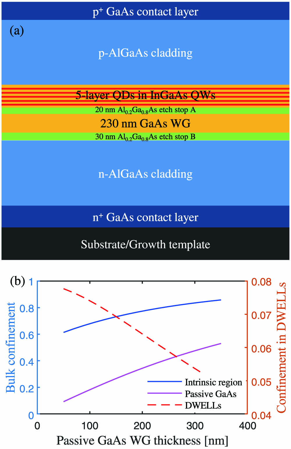
Fig. 1. (a) Schematic diagram of the epitaxial structure of OQD devices. (b) Optical confinement as functions of passive GaAs WG thickness.
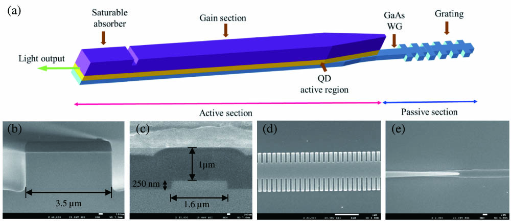
Fig. 2. (a) Schematic diagram of OQD MLL above the bottom cladding. The rendering is not to scale. The WG spiral termination is not illustrated here for simplicity. Scanning electron microscope (SEM) images of (b) mesa cross section after the nonselective GaAs etch, (c) passive GaAs WG cross section with 1 μm thick silicon dioxide upper cladding, (d) GaAs WG with gratings etched on the sidewall, and (e) taper transition from the active to the passive WG section.
Fig. 3. (a) Reflectivities and (b) group delay responses of several grating designs simulated with the transmission matrix technique. Red: uniform grating, κ = 162 cm − 1 CR = − 0.032 nm / μm CR = − 0.032 nm / μm κ = 162 cm − 1 κ = 243 cm − 1
Fig. 4. (a) CW LIV curves for 20 GHz OQD MLL with SA in a floating state. Blue: laser A. Pink: laser B. Green: laser C. (b) Optical spectra under the bias conditions I gain = 129 mA V SA = 5.6 V
Fig. 5. Pulse width mapping as a function of gain section current and SA section reverse bias voltage under passive mode-locking operation for laser C. Regions marked by white indicate unsuccessful PML.
Fig. 6. (a) Autocorrelator traces of the narrowest pulses of OQD MLLs with various grating designs. Blue, red, green, pink, and brown circles represent lasers A–E, respectively. Sech 2 I gain = 129 mA V SA = 5.6 V
|
Table 1. MLL Design and Performance Parameters

Set citation alerts for the article
Please enter your email address
© Copyright 2018-2021 | Chinese Laser Press. All Rights Reserved 沪ICP备15018463号-20