
Yu-Qiang GU, Ming TAN, Yuan-Yuan WU, Jian-Ya LU, Xue-Fei LI, Shu-Long LU. InAlAs/InGaAs avalanche photodiode with an optimized multiplication layer[J]. Journal of Infrared and Millimeter Waves, 2021, 40(6): 715
- Journal of Infrared and Millimeter Waves
- Vol. 40, Issue 6, 715 (2021)
Abstract
Introduction
Over the past decades,avalanche photodiodes (APDs)have been widely used for commercial,military and scientific research[
Gain-bandwidth product (GBP)is an important characteristic of APDs for application in high-speed transmission,however,a device with high GBP often results in a high dark current,which is closely related to the thickness of the multiplication layer. M.Nada et al. reported that an APD device with a higher bandwidth in the case of a thinner multiplication layer was obtained. However,the dark current of the device will also increase with decreasing multiplication layer [
In this paper,we designed a mesa InAlAs/InGaAs APD with an optimized 200 nm InAlAs multiplication layer. The electric field distribution,current-voltage (I-V)characteristics,capacitance-voltage (C-V)characteristics,gain characteristics and frequency characteristic are calculated by Silvaco Atlas tool. The fabricated InGaAs/InAlAs APD with a diameter of 30 μm exhibits low dark current of 19 nA at 0.9 Vb and high gain-bandwidth product about 155 GHz. The experiment results show a good agreement with the calculation.
1 Device design and calculation
A two-dimensional model of InAlAs/InGaAs separate absorption,grading,charge and multiplication (SAGCM)APD is established on the basis of the calculation of the device by using the Atlas Silvaco. The calculation is based on the drift-diffusion model,the Poisson equation and carrier continuity equation to calculate the electrical and optical performance. In order to make the device calculation results closer to the actual operating mode,the calculation process follows assumptions and simplifications [
1. P+-N is an abrupt junction
| Parameters | Units | InGaAs | InAlAs |
|---|---|---|---|
| Band gap | eV | 0.75 | 1.42 |
| Align | 0.36 | 0.36 | |
| Permittivity | 13.9 | 12.2 | |
| Electron SRH lifetime | s | 4×10⁻⁸ | 1×10-18 |
| Hole SRH lifetime | s | 4×10⁻⁸ | 1×10-18 |
| Electron mobility | cm2/V·s | 10 000 | 3 000 |
| Hole mobility | cm2/V·s | 150 | 250 |
| Radiative recombination coefficient | cm3/s | 9.6×10⁻¹ | 1.2×10⁻¹⁰ |
Table 1. Material parameters used in SILVACO physical modeling
2. The multiplication,charge,grading and absorption layers are uniform doping
3. The absorption layer is completely depleted at punch-through voltage
The physical models used in the calculation including the Shockley-Read-Hall Recombination (SRH),Auger Recombination (AUGER),Optical Radiative Recombination (OPTR)and Impact Ionization Model (IMPACT). In addition,the Fermi-Dirac model is used for the static characteristics of the carrier,and the high field saturation model is used to consider the effect of mobility reduction under high electric field. Ray tracing model is utilized for calculating optical characteristic. Newton's numerical iterative analysis method is used to derive the solutions of Poisson equation and continuity equation. Specific model information can refer to the following literatures[
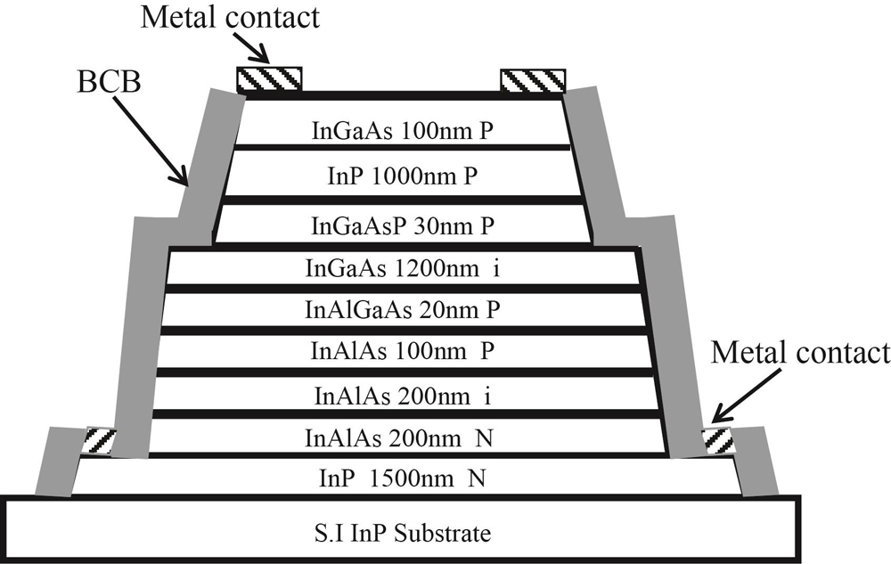
![]()
Figure 1.Structure of InAlAs/InGaAs APD
In APDs,the bandwidth can be expressed as
where τ is the response time,τRC is the RC time constant,τt is the carrier transit time,τa is the avalanche build-up time.
The RC time constant is determined by the depletion region capacitance C,the device series resistance and the load resistance R. As we can see from the
where R is total resistance of the device,C is the depletion region capacitance C,ε is the dielectric constant,A is the PN junction area,W is the width of depletion region.
The transit time includes the following processes:The photo-induced carriers separate in the InGaAs absorption layer and the electrons drift to the InAlAs multiplication layer under the external electric field. Then electron-hole pairs are produced by impact ionization. The electrons transfer to the N metal and the holes transfer to the P metal.
The avalanche build-up time increases when the thickness of multiplication layer decreases. Compared with carry drift time and RC time constant,avalanche multiplication time is dominant. So the thickness of other layers has little effect on GBP because of high gain of APDs. It is very important to design a reasonable thickness of multiplication layer.
The calculated 3-dB bandwidth is shown in
![]()
Figure 2.(a)The 3-dB bandwidth vs multiplication factor with different multiplication layer thickness,and (b)the gain-bandwidth product vs multiplication layer thickness
The tunneling current is a dominant component of the leakage current at high fields. Tunneling processes include direct band-to-band tunneling (BBT)and trap-assisted tunneling (TAT)[
where E is the electric field,Eg is the bandgap,m* is the effective mass and ћ is the Planck’s constant. It can be seen from
![]()
Figure 3.Distribution of electric field as a function of multiplication layer thickness
2 Device fabrication
The device was grown by using Molecular Beam Epitaxy (MBE)on a 350 μm semi-insulating InP substrate. Silicon and beryllium are used as n- and p-doping sources. All epitaxial layers are lattice matched to InP (001)substrate without off-orientation. The growth temperature is 480 ℃,which is monitored by pyrometer. The growth rate is 1um/h. A typical 2×1 reflective high-energy electron diffraction (RHEED)pattern is observed for InGaAs and InGaAsP growth and a 2×4 pattern for InP growth. Doping level in film is confirmed by Hall measurement. The mole fraction is calibrated by beam flux pressure (BEP)and X-ray diffraction (XRD). The actual epitaxial structure is as same as the calculated one. A 1.5 μm n-doped InP buffer layer is followed by a n-doped InAlAs layer. An intrinsic InAlAs multiplication layer (0.2 μm),a p-doped InAlAs charge layer (0.1 μm),a 0.02 μm InAlGaAs grading layer,a 1.2 μm intrinsic absorption layer,a p-doped InGaAsP grading layer (0.03 μm),a p-doped InP layer (1.0 μm)and a 0.1 μm p+ doped contact layer.
The mesa type APD is fabricated using standard photolithography,lift-off,wet chemical etching and styrene-acrylic cyclobutene (BCB)passivation. Compared with dry etching,wet etching has less damage to the surface of the device and can reduce surface leakage of the device. Then BCB was coated on the surface of the device and cured at 250 °C for 1 h to form passivation protection on the sidewall of the device. SiNx is selected as the antireflection film,and the active region is formed by lithographically. Finally,the metal is deposited on the anode and cathode.
3 Results and discussion
The measured and calculated dark and photocurrent are shown in
![]()
Figure 4.(a)Measured and Calculated I-V characteristic,(b)multiplication gain vs voltage,and (c)C-V characteristic of the InAlAs/InGaAs APD
The most important phenomenon to be considered in the calculation of dark current (Id)is the avalanche process,which is expressed as
among them,Id is the total dark current,Igr is the generation-recombination current,It is the tunneling current which is decided by the electrical field and band gap. Idu is the non-multiplied dark current,which is mainly from the surface of the device. M is the multiplication factor of the APD,M*is the avalanche gain of tunneling dark current.
The calculation of photocurrent (Ip)should consider the generation of electron-hole pairs in the absorption layer and the distribution of electric field both in the charge layer and the multiplication layer. The generation rate of electron-hole pairs produced by impact ionization carriers uses
where G is the generation rate of electron-hole pairs, αn and αp are the impact ionization coefficients of electrons and holes,respectively. Jn and Jp are the current densities of electrons and holes.
The gain of the device is obtained according to the
M is the multiplication factor ,where Il
Under dark condition,no electron-hole pairs are generated and no electrons are injected into the multiplication area. Therefore,the dark current changes little before and after the punch-through voltage (Vp). When the voltage is less than Vp,the photocurrent is close to the dark current. The impact ionization occurs due to carriers are injected into the multiplication layer when bias voltage reaches Vp,which lead to the photocurrent rises. When bias voltage approaches the breakdown voltage (Vb= 28.6 V),the photocurrent rapidly increases to 0.1 mA. In
The capacitance-voltage (C-V)characteristic is also particularly important for device structure design and performance evaluation. The actual total capacitance of the SAGCM APD device includes junction capacitance and parasitic capacitance. The parasitic capacitance mainly comes from the metal electrode. The effect of parasitic capacitance is not considered in the calculation process,so the calculated result is smaller than the actual capacitance. The C-V characteristic curve of the device is shown in
It can be seen from
The width of the depletion region does not change with the reverse bias voltage when the bias voltage greater than Vp,that is,the device is in a completely depleted state. The actual capacitance of the device is 68.7 pF. It can be seen that the calculated and actual Vp are 11.8V and 12.2V respectively,which matches well with value obtained from the I-V characteristics. The bandwidth of the APD detector is closely related to the RC time constant,and the response speed and bandwidth of the device can be improved by reducing the capacitance of the APD.
The frequency response test was analyzed by using a nonlinear vector network analyzer. We measured its frequency response from 20 MHz to 15 GHz at 1550 nm. In order to obtain the theoretical maximum bandwidth,we calculated the 3-dB bandwidth at different voltage. As we can see from Fig.
![]()
Figure 5.3-dB bandwidth vs voltage
![]()
Figure 6.(a)Measured and Calculated frequency characteristic,and (b)3-dB bandwidth vs multiplication gain of fabricated InAlAs/InGaAs APD
4 Conclusion
In this paper,an InAlAs/InGaAs APD with SAGCM structure was designed. The quantitative and predictive physical model with the operation of the device was established. The fabricated device bandwidth was 7.6 GHz and the GBP reached 155 GHz while the dark current was only 19 nA (at 90% Vb). However,since the parameters adopted in the simulation are too ideal and the effect of the process of device fabrication on the device performance is not considered,the simulated results are far away from the experimental results. A real material parameter as well as a less effect of the device fabrication is needed in the following work. This study is significant to the future high-speed transmission application of the avalanche photodiodes.
References
[3] N Bertone, W Clark. Avalanche photodiode arrays provide versatility in ultrasensitive applications. Laser Focus World, 43, 69(2007).
[4] R Mitra, J D Beck, M R Skokan et al. Intelligent Integrated Microsystems(2006).
[7] Yong-Fu LI, Jun-Liang LIU, Qing-Pu WANG et al. Avalanche characterization of high speed single-photon detector based on InGaAs/InP APD. J.Infrared Millim.Waves, 34, 427-431(2015).
[8] Bin LI, Wei CHEN, Xiao-Feng HUANG et al. InP cap layer doping density in InGaAs/InP single-photon avalanche diode. J.Infrared Millim.Waves, 36, 420-424(2017).
[17] J W Parks, K F Brennan, L E J V D Tarof. Macroscopic device simulation of InGaAs/InP based avalanche photodiodes, 6, 79-82(2014).
[19] Y Matsushima, K Sakai, Y J I E D L Noda. New type InGaAs/InP heterostructure avalanche photodiode with buffer layer, 2, 179-181(2005).
[21] Yu-Shun CHENG, Hui-Jun GUO, Hao LI et al. Device design pf planner PIN HgCdTe avalanche photodiode. J.Infrared Millim.Waves, 39, 8-14(2020).

Set citation alerts for the article
Please enter your email address
© Copyright 2018-2021 | Chinese Laser Press. All Rights Reserved 沪ICP备15018463号-20